


 Loading...
ML605 Hardware
User Guide
User Guide [optional]
UG534 (v1.2.1) January 21, 2010 [optional]

Xilinx is disclosing this user guide, manual, release note, and/or specification (the "Documentation") to you solely for use in the development of designs to operate with Xilinx hardware devices. You may not reproduce, distribute, republish, download, display, post, or transmit the Documentation in any form or by any means including, but not limited to, electronic, mechanical, photocopying, recording, or otherwise, without the prior written consent of Xilinx. Xilinx expressly disclaims any liability arising out of your use of the Documentation. Xilinx reserves the right, at its sole discretion, to change the Documentation without notice at any time. Xilinx assumes no obligation to correct any errors contained in the Documentation, or to advise you of any corrections or updates. Xilinx expressly disclaims any liability in connection with technical support or assistance that may be provided to you in connection with the Information.
THE DOCUMENTATION IS DISCLOSED TO YOU “AS-IS” WITH NO WARRANTY OF ANY KIND. XILINX MAKES NO OTHER WARRANTIES, WHETHER EXPRESS, IMPLIED, OR STATUTORY, REGARDING THE DOCUMENTATION, INCLUDING ANY WARRANTIES OF MERCHANTABILITY, FITNESS FOR A PARTICULAR PURPOSE, OR NONINFRINGEMENT OF THIRD-PARTY RIGHTS. IN NO EVENT WILL XILINX BE LIABLE FOR ANY CONSEQUENTIAL, INDIRECT, EXEMPLARY, SPECIAL, OR INCIDENTAL DAMAGES, INCLUDING ANY LOSS OF DATA OR LOST PROFITS, ARISING FROM YOUR USE OF THE DOCUMENTATION.
© 2009–2010 Xilinx, Inc. XILINX, the Xilinx logo, Virtex, Spartan, ISE, and other designated brands included herein are trademarks of Xilinx in the United States and other countries. All other trademarks are the property of their respective owners. PCI, PCI Express, PCIe, and PCI-X are trademarks of PCI-SIG.
Revision History
The following table shows the revision history for this document.
Date |
Version |
Revision |
|
|
|
8/17/09 |
1.0 |
Initial Xilinx release. |
|
|
|
11/17/09 |
1.1 |
• Updated Figure 1-1, Figure 1-2, Figure 1-3, Figure 1-11, and Figure 1-14. |
|
|
• Added Figure 1-7, Figure 1-8, Figure 1-10, and Figure 1-13. |
|
|
• Updated Table 1-15 and Table 1-18. |
|
|
• Updated Appendix B, “VITA 57.1 FMC LPC (J63) and HPC (J64) Connector Pinout” |
|
|
and Appendix C, “ML605 Master UCF.” |
|
|
• Minor typographical edits. |
|
|
|
01/15/10 |
1.2 |
• Updated Figure 1-2, Figure 1-3, Figure 1-17, Table 1-3, Table 1-8, Table 1-9, Table A-1, |
|
|
and Table A-2. Miscellaneous typographical edits. |
|
|
|
1/21/10 |
1.2.1 |
• Corrected typos in Table 1-31 and Figure 1-28. |
|
|
|
ML605 Hardware User Guide |
www.xilinx.com |
UG534 (v1.2.1) January 21, 2010 |

Table of Contents
Preface: About This Guide
Guide Contents . . . . . . . . . . . . . . . . . . . . . . . . . . . . . . . . . . . . . . . . . . . . . . . . . . . . . . . . . . . . . . 5
Additional Documentation . . . . . . . . . . . . . . . . . . . . . . . . . . . . . . . . . . . . . . . . . . . . . . . . . . . 5
Additional Support Resources. . . . . . . . . . . . . . . . . . . . . . . . . . . . . . . . . . . . . . . . . . . . . . . . 6
Chapter 1: ML605 Evaluation Board
Overview . . . . . . . . . . . . . . . . . . . . . . . . . . . . . . . . . . . . . . . . . . . . . . . . . . . . . . . . . . . . . . . . . . . . 7
Additional Information . . . . . . . . . . . . . . . . . . . . . . . . . . . . . . . . . . . . . . . . . . . . . . . . . . . . . 7
Features . . . . . . . . . . . . . . . . . . . . . . . . . . . . . . . . . . . . . . . . . . . . . . . . . . . . . . . . . . . . . . . . . . 8
Block Diagram . . . . . . . . . . . . . . . . . . . . . . . . . . . . . . . . . . . . . . . . . . . . . . . . . . . . . . . . . . . 10
Related Xilinx Documents. . . . . . . . . . . . . . . . . . . . . . . . . . . . . . . . . . . . . . . . . . . . . . . . . . . 10
Detailed Description . . . . . . . . . . . . . . . . . . . . . . . . . . . . . . . . . . . . . . . . . . . . . . . . . . . . . . . . 11
1. Virtex-6 XC6VLX240T-1FFG1156 FPGA . . . . . . . . . . . . . . . . . . . . . . . . . . . . . . . . . . . . 13
Configuration . . . . . . . . . . . . . . . . . . . . . . . . . . . . . . . . . . . . . . . . . . . . . . . . . . . . . . . . . 13
I/O Voltage Rails . . . . . . . . . . . . . . . . . . . . . . . . . . . . . . . . . . . . . . . . . . . . . . . . . . . . . . 14
2. 512 MB DDR3 Memory SODIMM . . . . . . . . . . . . . . . . . . . . . . . . . . . . . . . . . . . . . . . . . 15
3. 128 Mb Platform Flash XL. . . . . . . . . . . . . . . . . . . . . . . . . . . . . . . . . . . . . . . . . . . . . . . . 20
4. 32 MB Linear BPI Flash . . . . . . . . . . . . . . . . . . . . . . . . . . . . . . . . . . . . . . . . . . . . . . . . . . 20
ML605 Flash Boot Options . . . . . . . . . . . . . . . . . . . . . . . . . . . . . . . . . . . . . . . . . . . . . . . 21
5. System ACE CF and CompactFlash Connector . . . . . . . . . . . . . . . . . . . . . . . . . . . . . . 24
6. USB JTAG . . . . . . . . . . . . . . . . . . . . . . . . . . . . . . . . . . . . . . . . . . . . . . . . . . . . . . . . . . . . . 26
7. Clock Generation . . . . . . . . . . . . . . . . . . . . . . . . . . . . . . . . . . . . . . . . . . . . . . . . . . . . . . . 27
Oscillator (Differential) . . . . . . . . . . . . . . . . . . . . . . . . . . . . . . . . . . . . . . . . . . . . . . . . . . 27
Oscillator Socket (Single-Ended, 2.5V) . . . . . . . . . . . . . . . . . . . . . . . . . . . . . . . . . . . . . . 27
SMA Connectors (Differential) . . . . . . . . . . . . . . . . . . . . . . . . . . . . . . . . . . . . . . . . . . . . 29
8. Multi-Gigabit Transceivers (GTX MGTs) . . . . . . . . . . . . . . . . . . . . . . . . . . . . . . . . . . . 31
9. PCI Express Endpoint Connectivity . . . . . . . . . . . . . . . . . . . . . . . . . . . . . . . . . . . . . . . 32
10. SFP Module Connector . . . . . . . . . . . . . . . . . . . . . . . . . . . . . . . . . . . . . . . . . . . . . . . . . 35
11. 10/100/1000 Tri-Speed Ethernet PHY . . . . . . . . . . . . . . . . . . . . . . . . . . . . . . . . . . . . 36
SGMII GTX Transceiver Clock Generation . . . . . . . . . . . . . . . . . . . . . . . . . . . . . . . . . . . 37
12. USB-to-UART Bridge. . . . . . . . . . . . . . . . . . . . . . . . . . . . . . . . . . . . . . . . . . . . . . . . . . . 39
13. USB Controller . . . . . . . . . . . . . . . . . . . . . . . . . . . . . . . . . . . . . . . . . . . . . . . . . . . . . . . . 40
14. DVI Codec . . . . . . . . . . . . . . . . . . . . . . . . . . . . . . . . . . . . . . . . . . . . . . . . . . . . . . . . . . . . 41
15. IIC Bus . . . . . . . . . . . . . . . . . . . . . . . . . . . . . . . . . . . . . . . . . . . . . . . . . . . . . . . . . . . . . . . 42
8 Kb NV Memory . . . . . . . . . . . . . . . . . . . . . . . . . . . . . . . . . . . . . . . . . . . . . . . . . . . . . . 44
16. Status LEDs . . . . . . . . . . . . . . . . . . . . . . . . . . . . . . . . . . . . . . . . . . . . . . . . . . . . . . . . . . . 45
Ethernet PHY Status LEDs . . . . . . . . . . . . . . . . . . . . . . . . . . . . . . . . . . . . . . . . . . . . . . . 46
FPGA INIT and DONE LEDs . . . . . . . . . . . . . . . . . . . . . . . . . . . . . . . . . . . . . . . . . . . . . 47
17. User I/O . . . . . . . . . . . . . . . . . . . . . . . . . . . . . . . . . . . . . . . . . . . . . . . . . . . . . . . . . . . . . 47
User LEDs . . . . . . . . . . . . . . . . . . . . . . . . . . . . . . . . . . . . . . . . . . . . . . . . . . . . . . . . . . . . 48
User Pushbutton Switches . . . . . . . . . . . . . . . . . . . . . . . . . . . . . . . . . . . . . . . . . . . . . . . 49
User DIP Switch . . . . . . . . . . . . . . . . . . . . . . . . . . . . . . . . . . . . . . . . . . . . . . . . . . . . . . . 50
User SMA GPIO . . . . . . . . . . . . . . . . . . . . . . . . . . . . . . . . . . . . . . . . . . . . . . . . . . . . . . . 51
LCD Display (16 Character x 2 Lines). . . . . . . . . . . . . . . . . . . . . . . . . . . . . . . . . . . . . . . 52
18. Switches . . . . . . . . . . . . . . . . . . . . . . . . . . . . . . . . . . . . . . . . . . . . . . . . . . . . . . . . . . . . . . 53
Power On/Off Slide Switch SW2 . . . . . . . . . . . . . . . . . . . . . . . . . . . . . . . . . . . . . . . . . . 53
ML605 Hardware User Guide |
www.xilinx.com |
3 |
UG534 (v1.2.1) January 21, 2010 |
|
|

FPGA_PROG_B Pushbutton SW4 (Active-Low). . . . . . . . . . . . . . . . . . . . . . . . . . . . . . . 54 SYSACE_RESET_B Pushbutton SW3 (Active-Low) . . . . . . . . . . . . . . . . . . . . . . . . . . . . 54 System ACE CF CompactFlash Image Select DIP Switch S1. . . . . . . . . . . . . . . . . . . . . . 55 Mode, Osc Enable, Boot EEPROM Select, and Addr Select DIP Switch S2 . . . . . . . . . . . 56 19. VITA 57.1 FMC HPC Connector . . . . . . . . . . . . . . . . . . . . . . . . . . . . . . . . . . . . . . . . . 57
20. VITA 57.1 FMC LPC Connector . . . . . . . . . . . . . . . . . . . . . . . . . . . . . . . . . . . . . . . . . . 63 21. Power Management . . . . . . . . . . . . . . . . . . . . . . . . . . . . . . . . . . . . . . . . . . . . . . . . . . . . 65 AC Adapter and Input Power Jack/Switch . . . . . . . . . . . . . . . . . . . . . . . . . . . . . . . . . . 65 Onboard Power Regulation . . . . . . . . . . . . . . . . . . . . . . . . . . . . . . . . . . . . . . . . . . . . . . 66 22. System Monitor . . . . . . . . . . . . . . . . . . . . . . . . . . . . . . . . . . . . . . . . . . . . . . . . . . . . . . . 68
Configuration Options . . . . . . . . . . . . . . . . . . . . . . . . . . . . . . . . . . . . . . . . . . . . . . . . . . . . . . 73
Appendix A: Default Switch and Jumper Settings
Appendix B: VITA 57.1 FMC LPC (J63) and HPC (J64) Connector Pinout Appendix C: ML605 Master UCF
Appendix D: References
4 |
www.xilinx.com |
ML605 Hardware User Guide |
|
|
UG534 (v1.2.1) January 21, 2010 |

Preface
About This Guide
This manual accompanies the Virtex®-6 FPGA ML605 Evaluation Board and contains information about the ML605 hardware and software tools.
Guide Contents
This manual contains the following chapters:
•Chapter 1, “ML605 Evaluation Board,” provides an overview of the embedded development board and details the components and features of the ML605 board.
•Appendix A, “Default Switch and Jumper Settings.”
•Appendix B, “VITA 57.1 FMC LPC (J63) and HPC (J64) Connector Pinout.”
•Appendix C, “ML605 Master UCF.”
•Appendix D, “References.”
Additional Documentation
The following documents are also available for download at
http://www.xilinx.com/support/documentation/virtex-6.htm.
•Virtex-6 Family Overview
The features and product selection of the Virtex-6 family are outlined in this overview.
•Virtex-6 FPGA Data Sheet: DC and Switching Characteristics
This data sheet contains the DC and Switching Characteristic specifications for the Virtex-6 family.
•Virtex-6 FPGA Packaging and Pinout Specifications
This specification includes the tables for device/package combinations and maximum I/Os, pin definitions, pinout tables, pinout diagrams, mechanical drawings, and thermal specifications.
•Virtex-6 FPGA Configuration Guide
This all-encompassing configuration guide includes chapters on configuration interfaces (serial and SelectMAP), bitstream encryption, boundary-scan and JTAG configuration, reconfiguration techniques, and readback through the SelectMAP and JTAG interfaces.
•Virtex-6 FPGA Clocking Resources User Guide
This guide describes the clocking resources available in all Virtex-6 devices, including the MMCM and PLLs.
ML605 Hardware User Guide |
www.xilinx.com |
5 |
UG534 (v1.2.1) January 21, 2010 |
|
|

Preface: About This Guide
•Virtex-6 FPGA Memory Resources User Guide
The functionality of the block RAM and FIFO are described in this user guide.
•Virtex-6 FPGA SelectIO Resources User Guide
This guide describes the SelectIO™ resources available in all Virtex-6 devices.
•Virtex-6 FPGA GTX Transceivers User Guide
This guide describes the GTX transceivers available in all Virtex-6 FPGAs except the XC6VLX760.
•Virtex-6 FPGA Embedded Tri-Mode Ethernet MAC User Guide
This guide describes the dedicated Tri-Mode Ethernet Media Access Controller available in all Virtex-6 FPGAs except the XC6VLX760.
•Virtex-6 FPGA DSP48E1 Slice User Guide
This guide describes the architecture of the DSP48E1 slice in Virtex-6 FPGAs and provides configuration examples.
•Virtex-6 FPGA System Monitor User Guide
The System Monitor functionality available in all Virtex-6 devices is outlined in this guide.
•Virtex-6 FPGA PCB Design Guide
This guide provides information on PCB design for Virtex-6 devices, with a focus on strategies for making design decisions at the PCB and interface level.
Additional Support Resources
To search the database of silicon and software questions and answers or to create a technical support case in WebCase, see the Xilinx website at:
http://www.xilinx.com/support.
6 |
www.xilinx.com |
ML605 Hardware User Guide |
|
|
UG534 (v1.2.1) January 21, 2010 |

Chapter 1
ML605 Evaluation Board
Overview
The ML605 board enables hardware and software developers to create or evaluate designs targeting the Virtex®-6 XC6VLX240T-1FFG1156 FPGA.
The ML605 provides board features common to many embedded processing systems. Some commonly used features include: a DDR3 SODIMM memory, an 8-lane PCI Express® interface, a tri-mode Ethernet PHY, general purpose I/O, and a UART. Additional user desired features can be added through mezzanine cards attached to the onboard high-speed VITA-57 FPGA Mezzanine Connector (FMC) high pin count (HPC) expansion connector, or the onboard VITA-57 FMC low pin count (LPC) connector.
“Features,” page 8 provides a general listing of the board features with details provided in “Detailed Description,” page 11.
Additional Information
Additional information and support material is located at:
•http://www.xilinx.com/ml605 This information includes:
•Current version of this user guide in PDF format
•Example design files for demonstration of Virtex-6 FPGA features and technology
•Demonstration hardware and software configuration files for the System ACE™ CF controller, Platform Flash configuration storage device, and linear flash chip
•Reference design files
•Schematics in PDF and DxDesigner formats
•Bill of materials (BOM)
•Printed-circuit board (PCB) layout in Allegro PCB format
•Gerber files for the PCB (Many free or shareware Gerber file viewers are available on the internet for viewing and printing these files.)
•Additional documentation, errata, frequently asked questions, and the latest news
For information about the Virtex-6 family of FPGA devices, including product highlights, data sheets, user guides, and application notes, see the Virtex-6 FPGA documentation page at http://www.xilinx.com/support/documentation/virtex-6.htm.
ML605 Hardware User Guide |
www.xilinx.com |
7 |
UG534 (v1.2.1) January 21, 2010 |
|
|

Chapter 1: ML605 Evaluation Board
Features
The ML605 provides the following features:
•1. Virtex-6 XC6VLX240T-1FFG1156 FPGA
•2. 512 MB DDR3 Memory SODIMM
•3. 128 Mb Platform Flash XL
•4. 32 MB Linear BPI Flash
•5. System ACE CF and CompactFlash Connector
•6. USB JTAG
•7. Clock Generation
♦Fixed 200 MHz oscillator (differential)
♦Socketed 2.5V oscillator (single-ended)
♦SMA connectors (differential)
♦SMA connectors for MGT clocking
•8. Multi-Gigabit Transceivers (GTX MGTs)
♦FMC - HPC connector
♦FMC - LPC connector
♦SMA
♦PCIe
♦SFP Module connector
♦Ethernet PHY SGMII interface
•9. PCI Express Endpoint Connectivity
♦Gen1 8-lane (x8)
♦Gen2 4-lane (x4)
•10. SFP Module Connector
•11. 10/100/1000 Tri-Speed Ethernet PHY
•12. USB-to-UART Bridge
•13. USB Controller
•14. DVI Codec
•15. IIC Bus
♦IIC EEPROM - 1 KB
♦DDR3 SODIMM socket
♦DVI CODEC
♦DVI connector
♦FMC HPC connector
♦FMC LPC connector
♦SFP module connector
8 |
www.xilinx.com |
ML605 Hardware User Guide |
|
|
UG534 (v1.2.1) January 21, 2010 |

Overview
•16. Status LEDs
♦Ethernet status
♦FPGA INIT
♦FPGA DONE
♦System ACE CF Status
•17. User I/O
♦USER LED Group 1 - GPIO (8)
♦USER LED Group 2 - directional (5)
♦User pushbuttons - directional (5)
♦CPU reset pushbutton
♦User DIP switch - GPIO (8-pole)
♦User SMA GPIO connectors (2)
♦LCD character display (16 characters x 2 lines)
•18. Switches
♦Power on/off slide switch
♦System ACE CF reset pushbutton
♦System ACE CF bitstream image select DIP switch
♦Configuration MODE DIP switch
•19. VITA 57.1 FMC HPC Connector
•20. VITA 57.1 FMC LPC Connector
•21. Power Management
♦PMBus voltage and current monitoring via TI power controller
♦22. System Monitor
•Configuration Options
♦3. 128 Mb Platform Flash XL
♦4. 32 MB Linear BPI Flash
♦5. System ACE CF and CompactFlash Connector
♦6. USB JTAG
ML605 Hardware User Guide |
www.xilinx.com |
9 |
UG534 (v1.2.1) January 21, 2010 |
|
|
Chapter 1: ML605 Evaluation Board
Block Diagram
Figure 1-1 shows a high-level block diagram of the ML605 and its peripherals.
System ACE CF |
|
|
|
JTAG USB Mini-B |
|
VITA 57.1 FMC |
|
VITA 57.1 FMC |
S.A. CompactFlash |
|
|
|
USB JTAG Circuit |
|
HPC Connector |
|
LPC Connector |
S.A. 8-bit MPU I/F |
|
|
|
|
|
|
|
|
|
|
|
|
|
|
|
|
|
|
|
|
|
|
|
|
|
|
|
|
|
|
|
|
|
|
|
|
|
|
|
|
|
|
|
|
|
Platform Flash |
|
|
|
|
BANK32 |
|
|
|
|
|
|
BANK12, 13 |
|
BANK15,16 |
|
|
|
|
SYSMON I/F |
||||||||
|
|
|
|
BANK24 |
|
|
|
|
|
|
BANK14,22 |
BANK34,116 |
|
|
|
|
INIT, DONE LEDs |
||||||||||
Linear BPI Flash |
|
|
|
|
|
|
|
|
|
|
|
|
|
|
|||||||||||||
|
|
|
|
|
|
|
|
|
|
BANK23,24 |
|
|
|
|
|
|
|
PROG PB, MODE SW |
|||||||||
|
|
|
|
|
|
|
|
BANK34 |
|
|
|
|
|
|
|
|
|
|
|
|
|
||||||
|
|
|
|
|
|
|
|
|
|
|
|
|
|
BANK112,113 |
|
|
BANK0 |
|
|
|
|
|
|||||
|
|
|
|
|
|
|
|
|
|
|
|
|
|
|
|
|
|
|
|
|
|
|
|||||
|
|
|
|
|
|
|
|
|
|
|
|
|
|
|
|
|
|
|
|
|
|
|
|
|
|
|
|
|
|
|
|
|
|
|
|
|
|
|
|
|
|
|
|
|
|
|
|
|
|
|
|
|
|
|
|
|
|
|
|
|
|
|
|
|
|
|
|
|
|
|
|
|
|
|
|
|
|
|
|
|
|
|
IIC Bus |
DVI Codec |
|
|
|
|
BANK32 |
|
|
|
|
|
|
|
|
|
|
|
BANK33 |
|
|
|
|
IIC EEPROM |
|||||
|
|
|
|
|
|
|
|
|
|
|
|
|
|
|
|
|
|
|
|||||||||
|
|
|
|
|
|
|
|
|
|
|
|
|
|
|
|
|
|
|
FMC HPC |
||||||||
VGA Video |
|
|
|
|
|
|
|
|
|
|
|
|
|
|
|
|
|
BANK34 |
|
|
|
|
|||||
|
|
|
|
|
|
|
|
|
|
Virtex-6 |
|
|
|
|
|
|
|
||||||||||
|
|
|
|
|
|
|
|
|
|
|
|
|
|
|
|
DDR3 SODIMM IIC |
|||||||||||
DVI Video Connector |
|
|
|
|
|
|
|
|
|
|
|
|
|
|
|
|
|
|
|||||||||
|
|
|
|
|
|
|
|
|
|
FPGA |
|
|
|
|
|
|
|
|
|
FMC LPC |
|||||||
|
|
|
|
|
|
|
|
|
|
|
|
|
|
|
|
|
|
|
|
|
|
|
|||||
|
|
|
|
|
|
|
|
|
|
|
|
XC6VLX240T - 1FFG1156 |
|
|
|
|
|
|
|
|
|
|
|||||
|
|
|
|
|
|
|
|
|
|
|
|
|
|
|
|
|
|
|
|
|
|
||||||
|
|
|
|
|
|
|
|
|
|
|
|
|
|
|
|
|
|
|
|
|
|
|
|
|
|
|
|
10/100/1000 |
|
|
|
|
|
BANK33 |
|
|
|
|
|
|
|
|
|
|
|
BANK116 |
|
|
|
|
SFP Module |
||||
Ethernet PHY |
|
|
|
|
|
|
|
|
|
|
|
|
|
|
|
|
|
|
|
Connector |
|||||||
|
|
|
|
|
|
|
|
|
|
|
|
|
|
|
|
|
|
|
|
|
|
|
|||||
MII/GMII/RMII |
|
|
|
|
|
|
|
|
|
|
|
|
|
|
|
|
|
|
|
|
|
|
|
SGMII |
|||
|
|
|
|
|
|
|
|
BANK 25, 35 |
|
|
|
|
|
|
|
BANK114 |
|
|
|
|
|
||||||
|
|
|
|
|
|
|
|
|
|
|
|
|
|
|
|
|
|
|
|
||||||||
SODIMM Socket |
|
|
|
|
BANK 26, 36 |
|
|
|
|
|
|
|
BANK115 |
|
|
|
PCIe X8 Edge Connector |
||||||||||
|
|
|
|
BANK14, 33, 36 BANK24,34 |
|
|
BANK14 |
|
|
|
|
|
|
|
|||||||||||||
204-pin, DDR3 |
|
|
|
|
|
|
|
|
BANK24 |
|
|
|
MGT SMA REF Clock |
||||||||||||||
Decoupling Caps |
|
|
|
|
|
|
|
|
|
|
|
|
|
|
|
|
|
|
|
|
|
|
MGT RX/TX SMA Port |
||||
|
|
|
|
|
|
|
|
|
|
|
|
|
|
|
|
|
|
|
|
|
|
||||||
|
|
|
|
|
|
|
|
|
|
|
|
|
|
|
|
|
|
|
|
|
|
|
|
|
|
||
|
|
|
|
|
|
|
|
|
|
|
|
|
|
|
|
|
|
|
|
|
|
|
|
|
|
|
|
|
|
|
|
|
|
|
|
|
|
|
|
|
|
|
|
|
|
|
|
|
|
|
|
|
|
|
|
|
|
|
|
|
|
|
|
|
|
|
|
|
|
|
|
|
|
|
|
|
|
|
|
|
|
|
|
MEM Vterm |
|
|
User LED/SW |
|
200 MHz LVDS Clock |
|
|
USB Controller |
|
|
CP2103 USB-TO-UART |
|
|||||||||||||||
|
|
User DIP SW |
|
SMA Clock |
|
|
Host Type “A” |
|
|
|
Bridge |
|
|
||||||||||||||
Regulator |
|
|
|
User LCD |
|
User S.E. 2.5V Clock |
|
|
Peripheral Mini-B |
|
|
USB Mini-B |
|
|
|||||||||||||
|
|
|
|
|
|
|
|
|
|
|
|
|
|
|
|
Connectors |
|
|
|
|
|
|
|
|
|
||
|
|
|
|
|
|
|
|
|
|
|
|
|
|
|
|
|
|
|
|
|
|
|
|
|
|
|
UG534_01_092709 |
|
|
|
|
|
|
|
|
|
|
|
|
|
|
|
|
|
|
|
|
|
|
|
|
|
|
|
|
|
|
|
|
|
|
|
|
|
|
|
|
|
|
|
|
|
|
|
|
|
|
|
|
|
|
|
|
Figure 1-1: ML605 High-Level Block Diagram
Related Xilinx Documents
Prior to using the ML605 Evaluation Board, users should be familiar with Xilinx resources. See Appendix D, “References” for a direct link to Xilinx documentation. See the following locations for additional documentation on Xilinx tools and solutions:
•ISE: www.xilinx.com/ise
•EDK: www.xilinx.com/edk
•Intellectual Property: www.xilinx.com/ipcenter
•Answer Browser: www.xilinx.com/support
10 |
www.xilinx.com |
ML605 Hardware User Guide |
|
|
UG534 (v1.2.1) January 21, 2010 |

Detailed Description
Detailed Description
Figure 1-2 shows a board photo with numbered features corresponding to Table 1-1 and the section headings in this document.
|
20 |
|
|
19 |
13 |
18a |
|
16c |
|
|
|
|
|
13 |
|||||
17a |
|
|
|
|
|
||||
|
|
|
|
|
|
21c |
|
||
|
|
|
|
|
|
|
23 |
||
|
10 |
|
|
|
|
|
|
||
|
|
|
|
|
|
|
|
||
|
|
|
|
|
|
|
|
|
|
17d |
7b |
7c |
17e |
18d |
18c |
|
16b |
|
|
|
|
|
|
|
|
|
|
|
|
|
|
|
|
|
|
|
21d |
|
5 |
|
2 |
|
|
|
|
|
|
|
|
|
|
|
|
|
|
18b |
|
|
|
12 |
|
|
|
|
|
|
|
|
|
|
|
|
|
|
|
|
|
|
|
6 |
7d |
|
|
|
|
|
|
|
|
|
|
|
|
|
|
|
|
|
|
16a |
|
|
|
|
|
|
|
|
|
|
|
1 |
|
|
|
|
|
|
|
|
11 |
|
|
22 |
21a |
|
|
|
21b |
|
|
|
|
|
|
|
|
||
|
8 |
|
|
|
|
|
|
|
|
|
|
|
|
|
|
|
|
|
|
|
3 |
|
|
|
|
|
|
|
|
|
|
17f |
|
21a |
|
17c |
|
|
|
14 |
8 |
|
|
|
|
|
|
|
|
|
4 |
|
|
|
|
|
17b |
|
|
|
|
|
|
|
|
|
|
|
|
|
9 |
7a |
|
|
|
|
|
|
|
|
|
(on backside) |
|
|
|
|
|
||
|
|
15 |
|
|
|
|
|
||
|
|
|
|
|
|
|
UG534_02_123009 |
||
Figure 1-2: ML605 Board Photo
The numbered features in Figure 1-2 correlate to the features and notes listed in Table 1-1.
Table 1-1: |
ML605 Features |
|
|
|
|
|
|
|
|
Number |
|
Feature |
Notes |
Schematic |
|
Page |
|||
|
|
|
|
|
|
|
|
|
|
1 |
|
Virtex-6 FPGA |
XC6VLX240T-1FFG1156 |
2 - 12 |
|
|
|
|
|
2 |
|
DDR3 SODIMM |
Micron 512 MB MT4JSF6464HY-1G1 |
15 |
|
|
|
|
|
3 |
|
128 Mb Platform Flash XL |
Xilinx XCF128X-FTG64C |
25 |
|
|
|
|
|
4 |
|
Linear BPI Flash |
Numonyx JS28F256P30T95 |
26 |
|
|
|
|
|
5 |
|
System ACE CF controller, CF |
Xilinx XCCACE-TQ144I |
13 |
|
connector |
(bottom of board) |
||
|
|
|
||
|
|
|
|
|
6 |
|
JTAG cable connector (USB |
USB JTAG download circuit |
46 |
|
Mini-B) |
|||
|
|
|
|
|
|
|
|
|
|
ML605 Hardware User Guide |
www.xilinx.com |
11 |
UG534 (v1.2.1) January 21, 2010 |
|
|

Chapter 1: ML605 Evaluation Board
Table 1-1: |
ML605 Features (Cont’d) |
|
|
|
|
|
|
|
|
Number |
|
Feature |
Notes |
Schematic |
|
Page |
|||
|
|
|
|
|
|
|
|
|
|
|
|
Clock generation |
200 MHz OSC, oscillator socket, SMA |
30 |
|
|
connectors |
||
|
|
|
|
|
|
|
|
|
|
|
|
a. 200 MHz oscillator (on |
Epson 200 MHz 2.5V LVDS OSC |
30 |
|
|
backside) |
||
|
|
|
|
|
7 |
|
|
|
|
|
b. Oscillator socket, single- |
MMD Components 66 MHz 2.5V |
30 |
|
|
|
ended |
|
|
|
|
|
|
|
|
|
c. SMA connectors |
SMA pair |
30 |
|
|
|
|
|
|
|
d. MGT REFCLK SMA |
SMA pair |
30 |
|
|
connectors |
||
|
|
|
|
|
|
|
|
|
|
8 |
|
GTX RX/TX port |
SMA x4 |
30 |
|
|
|
|
|
9 |
|
PCIe Gen1 (8-lane), |
Card edge connector, 8-lane |
21 |
|
Gen2 (4-lane) |
|||
|
|
|
|
|
|
|
|
|
|
10 |
|
SFP connector and cage |
AMP 136073-1 |
23 |
|
|
|
|
|
11 |
|
Ethernet (10/100/1000) with |
Marvell M88E1111 EPHY |
24 |
|
SGMII |
|||
|
|
|
|
|
|
|
|
|
|
12 |
|
USB Mini-B, USB-to-UART |
Silicon Labs CP2103GM bridge |
33 |
|
bridge |
|||
|
|
|
|
|
|
|
|
|
|
13 |
|
USB-A Host, USB Mini-B |
Cypress CY7C67300-100AXI |
27 |
|
peripheral connectors |
controller |
||
|
|
|
||
|
|
|
|
|
14 |
|
Video - DVI connector |
Chrontel CH7301C-TF Video codec |
28, 29 |
|
|
|
|
|
15 |
|
IIC NV EEPROM, 8 Kb |
ST Microelectronics M24C08- |
32 |
|
(on backside) |
WDW6TP |
||
|
|
|
||
|
|
|
|
|
|
|
Status LEDs |
|
13, 24, 31 |
|
|
|
|
|
|
|
a. Ethernet status |
Right-angle link rate and direction |
24 |
16 |
|
|
LEDs |
|
|
|
|
||
|
|
|
|
|
|
|
b. FPGA INIT, DONE |
Init (red), Done (green) |
31 |
|
|
|
|
|
|
|
c. System ACE CF status |
Status (green), Error (red) |
13 |
|
|
|
|
|
|
|
User I/O |
|
31 |
|
|
|
|
|
|
|
a. User LEDs, green (8) |
User I/O (active-High) |
30, 31, 33 |
|
|
|
|
|
|
|
b. User pushbuttons, N.O. |
User I/O (active-High) |
31 |
|
|
momentary (5) |
||
|
|
|
|
|
|
|
|
|
|
17 |
|
c. User LEDs, green (5) |
User I/O (active-High) |
31 |
|
|
|
|
|
|
|
d. User DIP switch (8-pole) |
User I/O (active-High) |
31 |
|
|
|
|
|
|
|
e. User GPIO SMA |
SMA pair |
30 |
|
|
connectors |
||
|
|
|
|
|
|
|
|
|
|
|
|
f. LCD 16 character x 2 line |
Displaytech S162D BA BC |
33 |
|
|
display |
||
|
|
|
|
|
|
|
|
|
|
12 |
www.xilinx.com |
ML605 Hardware User Guide |
|
|
UG534 (v1.2.1) January 21, 2010 |

|
|
|
|
|
|
Detailed Description |
|
|
|
|
|
|
|
|
|
|
|
|
Table 1-1: |
ML605 Features (Cont’d) |
|
|
|
|
|
|
|
|
|
|
|
|
|
|
Number |
|
Feature |
Notes |
Schematic |
|
|
|
|
Page |
|||
|
|
|
|
|
|
|
|
|
|
|
|
|
|
|
|
|
|
|
|
|
Switches |
|
13, 25, 39 |
|
|
|
|
|
|
|
|
|
|
|
|
|
a. Power On/Off |
Slide switch |
39 |
|
|
|
|
|
|
|
|
|
|
|
|
|
b. FPGA_PROG_B |
active-Low |
13 |
|
|
|
18 |
|
pushbutton |
||
|
|
|
|
||||
|
|
|
|
|
|
|
|
|
|
|
|
|
c. System ACE CF Image |
4-pole DIP switch (active-High) |
25 |
|
|
|
|
|
Select |
||
|
|
|
|
|
|
|
|
|
|
|
|
|
|
|
|
|
|
|
|
|
d. Mode Switch |
6-pole DIP switch (active-High) |
25 |
|
|
|
|
|
|
||
|
|
|
19 |
|
FMC - HPC connector |
Samtec ASP-134486-01 |
16 -19 |
|
|
|
|
|
|
||
|
|
|
20 |
|
FMC - LPC connector |
Samtec ASP-134603-01 |
20 |
|
|
|
|
|
|
|
|
|
|
|
|
|
Power management |
|
35 - 44 |
|
|
|
|
|
|
|
|
|
|
|
|
|
a. PMBus controllers |
2 x TI UCD9240PFC |
35, 40 |
|
|
|
|
|
|
|
|
|
|
|
|
|
b. Voltage regulators |
2 x PTD08A020W, 3 x PTD08A010W |
36-38, 43, |
|
|
|
|
|
|
44 |
|
|
|
|
21 |
|
|
|
|
|
|
|
|
|
|||
|
|
|
|
|
c. 12V power input |
6-pin Molex mini-fit connector |
39 |
|
|
|
|
|
connector |
||
|
|
|
|
|
|
|
|
|
|
|
|
|
|
|
|
|
|
|
|
|
d. 12V power input |
4-pin ATX disk type connector |
39 |
|
|
|
|
|
connector |
||
|
|
|
|
|
|
|
|
|
|
|
|
|
|
|
|
|
|
|
22 |
|
System Monitor Interface |
2x6 DIP male pin header |
34 |
|
|
connector |
|||||
|
|
|
|
|
|
|
|
|
|
|
|
|
|
|
|
|
|
|
23 |
|
System ACE Error DS30 LED |
Jumper on = enable LED |
13 |
|
|
disable jumper J69 |
Jumper off = disable LED |
||||
|
|
|
|
|
|
||
|
|
|
|
|
|
|
|
1. Virtex-6 XC6VLX240T-1FFG1156 FPGA
A Virtex-6 XC6VLX240T-1FFG1156 FPGA is installed on the embedded development board.
Keep-Out areas and drill holes are defined around the FPGA to support an Ironwood
Electronics SG-BGA-6046 FPGA socket.
References
See the Virtex-6 FPGA Data Sheet. [Ref 4]
Configuration
The ML605 supports configuration in the following modes:
•Slave SelectMAP (using Platform Flash XL with the onboard 47 MHz oscillator)
•Master BPI-Up (using Linear BPI Flash device)
•JTAG (using the included USB-A to Mini-B cable)
•JTAG (using System ACE CF and CompactFlash card)
ML605 Hardware User Guide |
www.xilinx.com |
13 |
UG534 (v1.2.1) January 21, 2010 |
|
|

Chapter 1: ML605 Evaluation Board
The ML605 supports Master BPI-Up, JTAG, and Slave SelectMAP. These are selected by setting M[2:0] options 010, 101 and 110 shown in Table 1-2.
Table 1-2: Virtex-6 FPGA Configuration Modes
Configuration Mode |
M[2:0] |
Bus Width(1) |
CCLK Direction |
Master Serial(2) |
000 |
1 |
Output |
Master SPI(2) |
001 |
1 |
Output |
Master BPI-Up(2) |
010 |
8, 16 |
Output |
Master BPI-Down(2) |
011 |
8, 16 |
Output |
Master SelectMAP(2) |
100 |
8, 16 |
Output |
JTAG |
101 |
1 |
Input (TCK) |
|
|
|
|
Slave SelectMAP |
110 |
8, 16, 32 |
Input |
|
|
|
|
Slave Serial(3) |
111 |
1 |
Input |
Notes:
1.The parallel configuration modes bus is auto-detected by the configuration logic.
2.In Master configuration mode, the CCLK pin is the clock source for the Virtex-6 FPGA internal configuration logic. The Virtex-6 FPGA CCLK output pin must be free from reflections to avoid double-clocking the internal configuration logic. See the Virtex-6 FPGA Configuration User Guide for more details. [Ref 5]
3.This is the default setting due to internal pull-up termination on mode pins.
For an overview on configuring the FPGA, see “Configuration Options,” page 73.
Note: The mode switches are part of DIP switch S2. The default mode setting (see Table A-1, page 75) is M[2:0]=010, which selects Master BPI-Up at board power-on. Switch S1 position 4 must be OFF to disable the System ACE controller from attempting to boot if a CF card is present.
References
See the Virtex-6 FPGA Configuration User Guide for detailed configuration information. [Ref 5]
I/O Voltage Rails
There are 16 I/O banks available on the Virtex-6 device. The voltage applied to the FPGA I/O banks used by the ML605 board is summarized in Table 1-3.
Table 1-3: Voltage Rails
|
U1 FPGA Bank |
I/O Rail |
Voltage |
|
|
|
|
|
|
|
Bank 0 |
VCC2V5_FPGA |
2.5V |
|
|
|
|
|
|
|
Bank 12(1) |
FMC_VIO_B_M2C |
2.5V |
|
|
Bank 13 |
VCC2V5_FPGA |
2.5V |
|
|
|
|
|
|
|
Bank 14 |
VCC2V5_FPGA |
2.5V |
|
|
|
|
|
|
|
Bank 15 |
VCC2V5_FPGA |
2.5V |
|
|
|
|
|
|
|
Bank 16 |
VCC2V5_FPGA |
2.5V |
|
|
|
|
|
|
|
Bank 22 |
VCC2V5_FPGA |
2.5V |
|
|
|
|
|
|
|
Bank 23 |
VCC2V5_FPGA |
2.5V |
|
|
|
|
|
|
|
|
|
|
|
14 |
|
www.xilinx.com |
ML605 Hardware User Guide |
|
|
|
|
UG534 (v1.2.1) January 21, 2010 |
|

Detailed Description
Table 1-3: Voltage Rails (Cont’d)
U1 FPGA Bank |
I/O Rail |
Voltage |
|
|
|
Bank 24 |
VCC2V5_FPGA |
2.5V |
|
|
|
Bank 25 |
VCC1V5_FPGA |
1.5V |
|
|
|
Bank 26 |
VCC1V5_FPGA |
1.5V |
|
|
|
Bank 32 |
VCC2V5_FPGA |
2.5V |
|
|
|
Bank 33 |
VCC2V5_FPGA |
2.5V |
|
|
|
Bank 34 |
VCC2V5_FPGA |
2.5V |
|
|
|
Bank 35 |
VCC1V5_FPGA |
1.5V |
|
|
|
Bank 36 |
VCC1V5_FPGA |
1.5V |
|
|
|
Notes:
1.The VITA 57.1 specification stipulates that the Bank 12 voltage named FMC_VIO_B_M2C is supplied by the FMC card plugged onto the relevant FMC connector (ML605 J64). FMC_VIO_B_M2C cannot exceed the base board (ML605) Vadj of the FMC connector. The ML605 FMC Vadj maximum is 2.5V.
References
See the Xilinx Virtex-6 FPGA documentation for more information at
http://www.xilinx.com/support/documentation/virtex-6.htm.
2. 512 MB DDR3 Memory SODIMM
A 512MB DDR3 SODIMM is provided as a flexible and efficient form-factor volatile memory for user applications. The ML605 SODIMM socket is wired to support a maximum SODIMM size of 2 GB.
The ML605 DDR3 64-bit wide interface has been tested to 800 MT/s.
The DDR3 interface is implemented in FPGA banks 25, 26, 35, and 36. DCI VRP/N resistor connections are only implemented banks 26 and 36. DCI functionality in banks 25 and 35 is achieved in the UCF by cascading DCI between adjacent banks as follows:
CONFIG DCI_CASCADE = "36 35";
CONFIG DCI_CASCADE = "26 25";
Table 1-4 shows the connections and pin numbers for the DDR3 SODIMM.
Table 1-4: DDR3 SODIMM Connections
U1 FPGA Pin |
Schematic Net Name |
J1 SODIMM |
|
|
|
||
|
|
Pin Number |
Pin Name |
|
|
|
|
L14 |
DDR3_A0 |
98 |
A0 |
|
|
|
|
A16 |
DDR3_A1 |
97 |
A1 |
|
|
|
|
B16 |
DDR3_A2 |
96 |
A2 |
|
|
|
|
E16 |
DDR3_A3 |
95 |
A3 |
|
|
|
|
D16 |
DDR3_A4 |
92 |
A4 |
|
|
|
|
J17 |
DDR3_A5 |
91 |
A5 |
|
|
|
|
ML605 Hardware User Guide |
www.xilinx.com |
15 |
UG534 (v1.2.1) January 21, 2010 |
|
|

Chapter 1: ML605 Evaluation Board
Table 1-4: DDR3 SODIMM Connections (Cont’d)
U1 FPGA Pin |
Schematic Net Name |
J1 SODIMM |
|
|
|
||
|
|
Pin Number |
Pin Name |
|
|
|
|
A15 |
DDR3_A6 |
90 |
A6 |
|
|
|
|
B15 |
DDR3_A7 |
86 |
A7 |
|
|
|
|
G15 |
DDR3_A8 |
89 |
A8 |
|
|
|
|
F15 |
DDR3_A9 |
85 |
A9 |
|
|
|
|
M16 |
DDR3_A10 |
107 |
A10/AP |
|
|
|
|
M15 |
DDR3_A11 |
84 |
A11 |
|
|
|
|
H15 |
DDR3_A12 |
83 |
A12_BC_N |
|
|
|
|
J15 |
DDR3_A13 |
119 |
A13 |
|
|
|
|
D15 |
DDR3_A14 |
80 |
A14 |
|
|
|
|
C15 |
DDR3_A15 |
78 |
A15 |
|
|
|
|
K19 |
DDR3_BA0 |
109 |
BA0 |
|
|
|
|
J19 |
DDR3_BA1 |
108 |
BA1 |
|
|
|
|
L15 |
DDR3_BA2 |
79 |
BA2 |
|
|
|
|
|
|
|
|
J11 |
DDR3_D0 |
5 |
DQ0 |
|
|
|
|
E13 |
DDR3_D1 |
7 |
DQ1 |
|
|
|
|
F13 |
DDR3_D2 |
15 |
DQ2 |
|
|
|
|
K11 |
DDR3_D3 |
17 |
DQ3 |
|
|
|
|
L11 |
DDR3_D4 |
4 |
DQ4 |
|
|
|
|
K13 |
DDR3_D5 |
6 |
DQ5 |
|
|
|
|
K12 |
DDR3_D6 |
16 |
DQ6 |
|
|
|
|
D11 |
DDR3_D7 |
18 |
DQ7 |
|
|
|
|
M13 |
DDR3_D8 |
21 |
DQ8 |
|
|
|
|
J14 |
DDR3_D9 |
23 |
DQ9 |
|
|
|
|
B13 |
DDR3_D10 |
33 |
DQ10 |
|
|
|
|
B12 |
DDR3_D11 |
35 |
DQ11 |
|
|
|
|
G10 |
DDR3_D12 |
22 |
DQ12 |
|
|
|
|
M11 |
DDR3_D13 |
24 |
DQ13 |
|
|
|
|
C12 |
DDR3_D14 |
34 |
DQ14 |
|
|
|
|
A11 |
DDR3_D15 |
36 |
DQ15 |
|
|
|
|
G11 |
DDR3_D16 |
39 |
DQ16 |
|
|
|
|
F11 |
DDR3_D17 |
41 |
DQ17 |
|
|
|
|
D14 |
DDR3_D18 |
51 |
DQ18 |
|
|
|
|
C14 |
DDR3_D19 |
53 |
DQ19 |
|
|
|
|
16 |
www.xilinx.com |
ML605 Hardware User Guide |
|
|
UG534 (v1.2.1) January 21, 2010 |

|
|
|
|
|
|
Detailed Description |
||
|
|
|
|
|
|
|
|
|
|
|
|
Table 1-4: DDR3 SODIMM Connections (Cont’d) |
|
|
|
|
|
|
|
|
|
|
|
|
|
|
|
|
|
U1 FPGA Pin |
Schematic Net Name |
J1 SODIMM |
|
||
|
|
|
|
|
|
|
||
|
|
|
|
|
Pin Number |
|
Pin Name |
|
|
|
|
|
|
|
|
|
|
|
|
|
G12 |
DDR3_D20 |
40 |
|
DQ20 |
|
|
|
|
|
|
|
|
|
|
|
|
|
G13 |
DDR3_D21 |
42 |
|
DQ21 |
|
|
|
|
|
|
|
|
|
|
|
|
|
F14 |
DDR3_D22 |
50 |
|
DQ22 |
|
|
|
|
|
|
|
|
|
|
|
|
|
H14 |
DDR3_D23 |
52 |
|
DQ23 |
|
|
|
|
|
|
|
|
|
|
|
|
|
C19 |
DDR3_D24 |
57 |
|
DQ24 |
|
|
|
|
|
|
|
|
|
|
|
|
|
G20 |
DDR3_D25 |
59 |
|
DQ25 |
|
|
|
|
|
|
|
|
|
|
|
|
|
E19 |
DDR3_D26 |
67 |
|
DQ26 |
|
|
|
|
|
|
|
|
|
|
|
|
|
F20 |
DDR3_D27 |
69 |
|
DQ27 |
|
|
|
|
|
|
|
|
|
|
|
|
|
A20 |
DDR3_D28 |
56 |
|
DQ28 |
|
|
|
|
|
|
|
|
|
|
|
|
|
A21 |
DDR3_D29 |
58 |
|
DQ29 |
|
|
|
|
|
|
|
|
|
|
|
|
|
E22 |
DDR3_D30 |
68 |
|
DQ30 |
|
|
|
|
|
|
|
|
|
|
|
|
|
E23 |
DDR3_D31 |
70 |
|
DQ31 |
|
|
|
|
|
|
|
|
|
|
|
|
|
G21 |
DDR3_D32 |
129 |
|
DQ32 |
|
|
|
|
|
|
|
|
|
|
|
|
|
B21 |
DDR3_D33 |
131 |
|
DQ33 |
|
|
|
|
|
|
|
|
|
|
|
|
|
A23 |
DDR3_D34 |
141 |
|
DQ34 |
|
|
|
|
|
|
|
|
|
|
|
|
|
A24 |
DDR3_D35 |
143 |
|
DQ35 |
|
|
|
|
|
|
|
|
|
|
|
|
|
C20 |
DDR3_D36 |
130 |
|
DQ36 |
|
|
|
|
|
|
|
|
|
|
|
|
|
D20 |
DDR3_D37 |
132 |
|
DQ37 |
|
|
|
|
|
|
|
|
|
|
|
|
|
J20 |
DDR3_D38 |
140 |
|
DQ38 |
|
|
|
|
|
|
|
|
|
|
|
|
|
G22 |
DDR3_D39 |
142 |
|
DQ39 |
|
|
|
|
|
|
|
|
|
|
|
|
|
D26 |
DDR3_D40 |
147 |
|
DQ40 |
|
|
|
|
|
|
|
|
|
|
|
|
|
F26 |
DDR3_D41 |
149 |
|
DQ41 |
|
|
|
|
|
|
|
|
|
|
|
|
|
B26 |
DDR3_D42 |
157 |
|
DQ42 |
|
|
|
|
|
|
|
|
|
|
|
|
|
E26 |
DDR3_D43 |
159 |
|
DQ43 |
|
|
|
|
|
|
|
|
|
|
|
|
|
C24 |
DDR3_D44 |
146 |
|
DQ44 |
|
|
|
|
|
|
|
|
|
|
|
|
|
D25 |
DDR3_D45 |
148 |
|
DQ45 |
|
|
|
|
|
|
|
|
|
|
|
|
|
D27 |
DDR3_D46 |
158 |
|
DQ46 |
|
|
|
|
|
|
|
|
|
|
|
|
|
C25 |
DDR3_D47 |
160 |
|
DQ47 |
|
|
|
|
|
|
|
|
|
|
|
|
|
C27 |
DDR3_D48 |
163 |
|
DQ48 |
|
|
|
|
|
|
|
|
|
|
|
|
|
B28 |
DDR3_D49 |
165 |
|
DQ49 |
|
|
|
|
|
|
|
|
|
|
|
|
|
D29 |
DDR3_D50 |
175 |
|
DQ50 |
|
|
|
|
|
|
|
|
|
|
|
|
|
B27 |
DDR3_D51 |
177 |
|
DQ51 |
|
|
|
|
|
|
|
|
|
|
|
|
|
G27 |
DDR3_D52 |
164 |
|
DQ52 |
|
|
|
|
|
|
|
|
|
|
|
|
|
A28 |
DDR3_D53 |
166 |
|
DQ53 |
|
|
|
|
|
|
|
|
|
|
|
|
|
|
|
|
|
|
|
ML605 Hardware User Guide |
www.xilinx.com |
|
17 |
|||||
UG534 (v1.2.1) January 21, 2010 |
|
|
|
|
|
|||

Chapter 1: ML605 Evaluation Board
Table 1-4: DDR3 SODIMM Connections (Cont’d)
U1 FPGA Pin |
Schematic Net Name |
J1 SODIMM |
|
|
|
||
|
|
Pin Number |
Pin Name |
|
|
|
|
E24 |
DDR3_D54 |
174 |
DQ54 |
|
|
|
|
G25 |
DDR3_D55 |
176 |
DQ55 |
|
|
|
|
F28 |
DDR3_D56 |
181 |
DQ56 |
|
|
|
|
B31 |
DDR3_D57 |
183 |
DQ57 |
|
|
|
|
H29 |
DDR3_D58 |
191 |
DQ58 |
|
|
|
|
H28 |
DDR3_D59 |
193 |
DQ59 |
|
|
|
|
B30 |
DDR3_D60 |
180 |
DQ60 |
|
|
|
|
A30 |
DDR3_D61 |
182 |
DQ61 |
|
|
|
|
E29 |
DDR3_D62 |
192 |
DQ62 |
|
|
|
|
F29 |
DDR3_D63 |
194 |
DQ63 |
|
|
|
|
E11 |
DDR3_DM0 |
11 |
DM0 |
|
|
|
|
B11 |
DDR3_DM1 |
28 |
DM1 |
|
|
|
|
E14 |
DDR3_DM2 |
46 |
DM2 |
|
|
|
|
D19 |
DDR3_DM3 |
63 |
DM3 |
|
|
|
|
B22 |
DDR3_DM4 |
136 |
DM4 |
|
|
|
|
A26 |
DDR3_DM5 |
153 |
DM5 |
|
|
|
|
A29 |
DDR3_DM6 |
170 |
DM6 |
|
|
|
|
A31 |
DDR3_DM7 |
187 |
DM7 |
|
|
|
|
|
|
|
|
E12 |
DDR3_DQS0_N |
10 |
DQS0_N |
|
|
|
|
D12 |
DDR3_DQS0_P |
12 |
DQS0_P |
|
|
|
|
J12 |
DDR3_DQS1_N |
27 |
DQS1_N |
|
|
|
|
H12 |
DDR3_DQS1_P |
29 |
DQS1_P |
|
|
|
|
A14 |
DDR3_DQS2_N |
45 |
DQS2_N |
|
|
|
|
A13 |
DDR3_DQS2_P |
47 |
DQS2_P |
|
|
|
|
H20 |
DDR3_DQS3_N |
62 |
DQS3_N |
|
|
|
|
H19 |
DDR3_DQS3_P |
64 |
DQS3_P |
|
|
|
|
C23 |
DDR3_DQS4_N |
135 |
DQS4_N |
|
|
|
|
B23 |
DDR3_DQS4_P |
137 |
DQS4_P |
|
|
|
|
A25 |
DDR3_DQS5_N |
152 |
DQS5_N |
|
|
|
|
B25 |
DDR3_DQS5_P |
154 |
DQS5_P |
|
|
|
|
G28 |
DDR3_DQS6_N |
169 |
DQS6_N |
|
|
|
|
H27 |
DDR3_DQS6_P |
171 |
DQS6_P |
|
|
|
|
D30 |
DDR3_DQS7_N |
186 |
DQS7_N |
|
|
|
|
18 |
www.xilinx.com |
ML605 Hardware User Guide |
|
|
UG534 (v1.2.1) January 21, 2010 |

|
|
|
|
|
|
Detailed Description |
||
|
|
|
|
|
|
|
|
|
|
|
|
Table 1-4: DDR3 SODIMM Connections (Cont’d) |
|
|
|
|
|
|
|
|
|
|
|
|
|
|
|
|
|
U1 FPGA Pin |
Schematic Net Name |
J1 SODIMM |
|
||
|
|
|
|
|
|
|
||
|
|
|
|
|
Pin Number |
|
Pin Name |
|
|
|
|
|
|
|
|
|
|
|
|
|
C30 |
DDR3_DQS7_P |
188 |
|
DQS7_P |
|
|
|
|
|
|
|
|
|
|
|
|
|
|
|
|
|
|
|
|
|
|
F18 |
DDR3_ODT0 |
116 |
|
ODT0 |
|
|
|
|
|
|
|
|
|
|
|
|
|
E17 |
DDR3_ODT1 |
120 |
|
ODT1 |
|
|
|
|
|
|
|
|
|
|
|
|
|
E18 |
DDR3_RESET_B |
30 |
|
RESET_B |
|
|
|
|
|
|
|
|
|
|
|
|
|
K18 |
DDR3_S0_B |
114 |
|
S0_B |
|
|
|
|
|
|
|
|
|
|
|
|
|
K17 |
DDR3_S1_B |
121 |
|
S1_B |
|
|
|
|
|
|
|
|
|
|
|
|
|
D17 |
DDR3_TEMP_EVENT |
198 |
|
EVENT_B |
|
|
|
|
|
|
|
|
|
|
|
|
|
B17 |
DDR3_WE_B |
113 |
|
WE_B |
|
|
|
|
|
|
|
|
|
|
|
|
|
C17 |
DDR3_CAS_B |
115 |
|
CAS_B |
|
|
|
|
|
|
|
|
|
|
|
|
|
L19 |
DDR3_RAS_B |
110 |
|
RAS_B |
|
|
|
|
|
|
|
|
|
|
|
|
|
M18 |
DDR3_CKE0 |
73 |
|
CKE0 |
|
|
|
|
|
|
|
|
|
|
|
|
|
M17 |
DDR3_CKE1 |
74 |
|
CKE1 |
|
|
|
|
|
|
|
|
|
|
|
|
|
H18 |
DDR3_CLK0_N |
103 |
|
CK0_N |
|
|
|
|
|
|
|
|
|
|
|
|
|
G18 |
DDR3_CLK0_P |
101 |
|
CK0_P |
|
|
|
|
|
|
|
|
|
|
|
|
|
L16 |
DDR3_CLK1_N |
104 |
|
CK1_N |
|
|
|
|
|
|
|
|
|
|
|
|
|
K16 |
DDR3_CLK1_P |
102 |
|
CK1_P |
|
|
|
|
|
|
|
|
|
|
The Memory Interface Generator (MIG) tool guidelines specify a set of U1 FPGA “No Connect” pins. These should be added to the UCF as CONFIG PROHIBIT pins as follows:
CONFIG PROHIBIT = H22;
CONFIG PROHIBIT = F21;
CONFIG PROHIBIT = B20;
CONFIG PROHIBIT = F19;
CONFIG PROHIBIT = C13;
CONFIG PROHIBIT = M12;
CONFIG PROHIBIT = L13;
CONFIG PROHIBIT = K14;
CONFIG PROHIBIT = F25;
CONFIG PROHIBIT = C29;
CONFIG PROHIBIT = C28;
CONFIG PROHIBIT = D24;
References
See the Micron Technology, Inc. for more information [Ref 22].
In addition, see the Virtex-6 FPGA Memory Interface Solutions User Guide [Ref 6] and the Virtex-6 FPGA Memory Resources User Guide [Ref 9].
ML605 Hardware User Guide |
www.xilinx.com |
19 |
UG534 (v1.2.1) January 21, 2010 |
|
|
Chapter 1: ML605 Evaluation Board
3. 128 Mb Platform Flash XL
A 128 Mb Xilinx XCF128X-FTG64C Platform Flash XL device is used with an onboard 47 MHz oscillator (X4) to configure the FPGA in less than 100 ms from power valid as required by the PCI Express Card Electromechanical Specification. This allows the PCIe interface to be recognized and enumerated when plugged into a host PC.
To achieve the fastest configuration speed, the FPGA mode pins are set to Slave SelectMAP and the onboard 47 MHz clock source external to the FPGA is used for configuration. Configuration DIP switch S2, switch 1, controls the 47 MHz oscillator enable as outlined in “18. Switches,” page 53.
See S2 switch setting details in Table 1-26, page 56. Also, see the “FPGA Design Considerations for the Configuration Flash,” page 23 for FPGA design recommendations.
4. 32 MB Linear BPI Flash
A Numonyx JS28F256P30 Linear BPI Flash memory (P30) on the ML605 provides 32 MB of non-volatile storage that can be used for configuration as well as software storage. The Linear BPI Flash shares the dual use configuration pins in parallel with the XCF128 Platform Flash XL.
The P30_CS net is used to select the P30 or the XCF128. Power-on configuration is selected by the P30_CS net which is tied to a dip switch S2 (selects pullup/pulldown) and is also wired to an FPGA non-config pin. The dip switch allows power selection for the configuration device P30 or XCF128XL. The dip switch selection can be overridden by the FPGA after configuration by controlling the logic level of the P30_CS signal.
See S2 switch setting details in Table 1-26, page 56. For an overview on configuring the FPGA, see “Configuration Options,” page 73.
Figure 1-3 shows a block diagram for the Platform Flash and BPI Flash.
|
|
|
|
|
|
U27 |
|
|
|
|
|
|
|
|
|
|
PLATFORM |
|
|||
|
|
|
|
|
|
FLASH |
|
|
|
|
FPGA U1 |
FLASH_A[22:0] |
A |
|
D |
|
|||||
|
|
|
|
|
|
|||||
Bank 34 |
|
|
|
|
|
|
|
|
|
|
|
|
|
|
|
|
|
|
|
|
|
S2 SWITCH 6 |
|
|
|
|
CE |
|
||||
|
|
|
|
|
|
|
|
|||
ON = U4 BPI Upper Half |
|
|
|
|
|
|
||||
OFF = U4 BPI Lower Half |
|
U4 |
|
|
|
|
||||
|
|
|
|
|
|
|
|
|
|
|
|
FLASH_A[23] |
|
BPI |
|
|
|
|
|||
FPGA U1 |
|
FLASH |
|
|
|
|
||||
|
|
|
|
|
|
|
|
|
|
|
Bank 24 |
|
|
|
|
|
|
|
|
|
|
VCC2V5 |
|
|
|
A |
|
D |
|
|||
|
|
|
|
|||||||
|
|
|
|
|
|
|
|
|||
510 |
|
S2-6 |
6 |
|
|
|
|
|
|
|
|
7 |
|
|
|
|
|
|
|
||
|
|
A23 |
|
E |
|
|||||
|
|
|
|
4.7K |
|
|
||||
|
|
|
|
|
|
|
|
|
||
|
|
|
|
|
|
|
|
|||
|
|
|
|
|
S1 Switch 4 |
||||
|
|
|
|
|
|
OFF = Disable System ACE, |
|||
|
|
|
|
|
|
|
|
enable U4/U27 flash boot |
|
|
|
|
|
|
|
ON = Enable System ACE boot when |
|||
FLASH_D[15:0] |
|
|
|
|
CF card is present |
||||
FPGA U1 |
|||||||||
VCC2V5 |
|
Bank 24 |
|||||||
|
|
|
|
|
|
U10 |
|||
|
|
|
|
6 |
|
|
|
|
|
PLATFLASH_FCS_B |
|
|
|
|
P30_CS_SEL |
||||
|
|
|
|
||||||
VCC2V5 |
|
|
|
|
|
|
|||
|
|
|
|
|
|
||||
|
|
|
|
|
|
(FPGA U1 pin AJ12) |
|||
|
|
|
|
|
|
|
|
|
|
510 S2-2 |
2 |
1 |
|
|
|
|
|
||
11 |
|
|
|
S2 SWITCH 2 |
|||||
|
|
|
|
|
|
|
|
||
|
|
|
|
4.7K |
|
|
|
ON = U4 BOOT |
|
|
|
|
|
|
|
|
OFF = U27 BOOT |
||
|
|
|
|
|
|
|
|
||
VCC2V5 |
|
|
|
|
|
|
|
||
|
|
|
|
4 |
|
|
|
3 FPGA_FCS_B FPGA U1 |
|
|
FLASH_CE_B |
|
|
|
|
Bank 24 |
|||
|
|
|
|
|
|
|
|
|
UG534_03_011110 |
Figure 1-3: Platform Flash and BPI Flash Block Diagram
20 |
www.xilinx.com |
ML605 Hardware User Guide |
|
|
UG534 (v1.2.1) January 21, 2010 |
Detailed Description
ML605 Flash Boot Options
The ML605 has two parallel wired flash memory devices as shown in Figure 1-3. At ML605 power-up, before FPGA configuration, DIP switch S2 switch 2 selects which flash device, U4 (BPI) or U27 (Platform Flash), provides the boot bitstream. Typically S2 switch 2 will be open/OFF to select the U27 Platform Flash. Given that the mode switches (S2 switch 3/M0, switch 4/M1 and switch 5/M2) are set to Slave SelectMAP mode, then U27, driven at 47 MHz, can load a PCIe core bitstream before a host PC motherboard can scan its PCIe slots.When S2 switch 2 is closed/ON at power up, the FPGA will be configured from the BPI flash device U4. Note that U4 address bit A23 is switched by S2 switch 6, which allows the lower or upper half of U4 to be chosen as a data source.
Table 1-5 shows the connections and pin numbers for the boot flash devices.
Table 1-5: Platform Flash and BPI Flash Connections
U1 FPGA Pin |
Schematic Net Name |
U4 BPI Flash |
U27 Platform Flash |
|||
|
|
|
|
|||
Pin Number |
Pin Name |
Pin Number |
Pin Name |
|||
|
|
|||||
|
|
|
|
|
|
|
AL8 |
FLASH_A0 |
29 |
A1 |
A1 |
A00 |
|
|
|
|
|
|
|
|
AK8 |
FLASH_A1 |
25 |
A2 |
B1 |
A01 |
|
|
|
|
|
|
|
|
AC9 |
FLASH_A2 |
24 |
A3 |
C1 |
A02 |
|
|
|
|
|
|
|
|
AD10 |
FLASH_A3 |
23 |
A4 |
D1 |
A03 |
|
|
|
|
|
|
|
|
C8 |
FLASH_A4 |
22 |
A5 |
D2 |
A04 |
|
|
|
|
|
|
|
|
B8 |
FLASH_A5 |
21 |
A6 |
A2 |
A05 |
|
|
|
|
|
|
|
|
E9 |
FLASH_A6 |
20 |
A7 |
C2 |
A06 |
|
|
|
|
|
|
|
|
E8 |
FLASH_A7 |
19 |
A8 |
A3 |
A07 |
|
|
|
|
|
|
|
|
A8 |
FLASH_A8 |
8 |
A9 |
B3 |
A08 |
|
|
|
|
|
|
|
|
A9 |
FLASH_A9 |
7 |
A10 |
C3 |
A09 |
|
|
|
|
|
|
|
|
D9 |
FLASH_A10 |
6 |
A11 |
D3 |
A10 |
|
|
|
|
|
|
|
|
C9 |
FLASH_A11 |
5 |
A12 |
C4 |
A11 |
|
|
|
|
|
|
|
|
D10 |
FLASH_A12 |
4 |
A13 |
A5 |
A12 |
|
|
|
|
|
|
|
|
C10 |
FLASH_A13 |
3 |
A14 |
B5 |
A13 |
|
|
|
|
|
|
|
|
F10 |
FLASH_A14 |
2 |
A15 |
C5 |
A14 |
|
|
|
|
|
|
|
|
F9 |
FLASH_A15 |
1 |
A16 |
D7 |
A15 |
|
|
|
|
|
|
|
|
AH8 |
FLASH_A16 |
55 |
A17 |
D8 |
A16 |
|
|
|
|
|
|
|
|
AG8 |
FLASH_A17 |
18 |
A18 |
A7 |
A17 |
|
|
|
|
|
|
|
|
AP9 |
FLASH_A18 |
17 |
A19 |
B7 |
A18 |
|
|
|
|
|
|
|
|
AN9 |
FLASH_A19 |
16 |
A20 |
C7 |
A19 |
|
|
|
|
|
|
|
|
AF10 |
FLASH_A20 |
11 |
A21 |
C8 |
A20 |
|
|
|
|
|
|
|
|
AF9 |
FLASH_A21 |
10 |
A22 |
A8 |
A21 |
|
|
|
|
|
|
|
|
AL9 |
FLASH_A22 |
9 |
A23 |
G1 |
A22 |
|
|
|
|
|
|
|
|
AA23 |
FLASH_A23 |
26 |
A24 |
NC |
A23 |
|
|
|
|
|
|
|
|
ML605 Hardware User Guide |
www.xilinx.com |
21 |
UG534 (v1.2.1) January 21, 2010 |
|
|

Chapter 1: ML605 Evaluation Board
Table 1-5: Platform Flash and BPI Flash Connections (Cont’d)
U1 FPGA Pin |
Schematic Net Name |
U4 BPI Flash |
U27 Platform Flash |
|||
|
|
|
|
|||
Pin Number |
Pin Name |
Pin Number |
Pin Name |
|||
|
|
|||||
|
|
|
|
|
|
|
|
|
|
|
|
|
|
AF24 |
FLASH_D0 |
34 |
DQ0 |
F2 |
DQ00 |
|
|
|
|
|
|
|
|
AF25 |
FLASH_D1 |
36 |
DQ1 |
E2 |
DQ01 |
|
|
|
|
|
|
|
|
W24 |
FLASH_D2 |
39 |
DQ2 |
G3 |
DQ02 |
|
|
|
|
|
|
|
|
V24 |
FLASH_D3 |
41 |
DQ3 |
E4 |
DQ03 |
|
|
|
|
|
|
|
|
H24 |
FLASH_D4 |
47 |
DQ4 |
E5 |
DQ04 |
|
|
|
|
|
|
|
|
H25 |
FLASH_D5 |
49 |
DQ5 |
G5 |
DQ05 |
|
|
|
|
|
|
|
|
P24 |
FLASH_D6 |
51 |
DQ6 |
G6 |
DQ06 |
|
|
|
|
|
|
|
|
R24 |
FLASH_D7 |
53 |
DQ7 |
H7 |
DQ07 |
|
|
|
|
|
|
|
|
G23 |
FLASH_D8 |
35 |
DQ8 |
E1 |
DQ08 |
|
|
|
|
|
|
|
|
H23 |
FLASH_D9 |
37 |
DQ9 |
E3 |
DQ09 |
|
|
|
|
|
|
|
|
N24 |
FLASH_D10 |
40 |
DQ10 |
F3 |
DQ10 |
|
|
|
|
|
|
|
|
N23 |
FLASH_D11 |
42 |
DQ11 |
F4 |
DQ11 |
|
|
|
|
|
|
|
|
F23 |
FLASH_D12 |
48 |
DQ12 |
F5 |
DQ12 |
|
|
|
|
|
|
|
|
F24 |
FLASH_D13 |
50 |
DQ13 |
H5 |
DQ13 |
|
|
|
|
|
|
|
|
L24 |
FLASH_D14 |
52 |
DQ14 |
G7 |
DQ14 |
|
|
|
|
|
|
|
|
M23 |
FLASH_D15 |
54 |
DQ15 |
E7 |
DQ15 |
|
|
|
|
|
|
|
|
|
|
|
|
|
|
|
J26 |
FLASH_WAIT |
56 |
WAIT |
NA(1) |
NA(1) |
|
AF23 |
FPGA_FWE_B |
14 |
/WE |
G8 |
/W |
|
|
|
|
|
|
|
|
AA24 |
FPGA_FOE_B |
32 |
/OE |
F8 |
/G |
|
|
|
|
|
|
|
|
K8 |
FPGA_CCLK |
NA(1) |
NA(1) |
F1 |
K |
|
AC23 |
PLATFLASH_L_B |
NA(1) |
NA(1) |
H1 |
/L |
|
Y24 |
FPGA_FCS_B(2) |
NA(1) |
NA(1) |
NA(1) |
NA(1) |
|
NA(1) |
PLATFLASH_FCS_B(3) |
NA(1) |
NA(1) |
B4 |
/E |
|
NA(1) |
FLASH_CE_B(4) |
30 |
/OE |
NA(1) |
NA(1) |
|
Notes:
1.Not Applicable
2.FPGA control flash memory select signal connected to pin U10.3
3.Platform Flash select signal connected to pin U10.6
4.BPI Flash select signal connected to pin U10.4
22 |
www.xilinx.com |
ML605 Hardware User Guide |
|
|
UG534 (v1.2.1) January 21, 2010 |

Detailed Description
FPGA Design Considerations for the Configuration Flash
After FPGA configuration, the FPGA design can disable the configuration flash or access the configuration flash to read/write code or data.
When the FPGA design does not use the configuration flash, the FPGA design must drive the FPGA FCS_B pin High in order to disable the configuration flash and put the flash into a quiescent, low-power state. Otherwise, the Platform Flash XL, in particular, can continue to drive its array data onto the data bus causing unnecessary switching noise and power consumption.
For FPGA designs that access the flash for reading/writing stored code or data, connect the FPGA design or EDK embedded memory controller (EMC) peripheral to the flash through the pins defined in Table 1-5, page 21.
The Platform Flash XL defaults to a synchronous read mode. Typically, the Platform Flash XL requires an initialization procedure to put the Platform Flash XL into the common, asynchronous read mode before accessing stored code or data. To put the Platform Flash XL into asynchronous read mode, apply the Set Configuration Register command sequence. See the Platform Flash XL High-Density Configuration and Storage Device Data Sheet for details on the Set Configuration Register command. [Ref 17]
References
See the Numonyx StrataFlash Embedded Memory Data Sheet. [Ref 24]
Visit the Xilinx Platform Flash product page and click the Resources tab for more information.
Also, see the Platform Flash XL High-Density Configuration and Storage Device Data Sheet [Ref 17] and the Virtex-6 Configuration User Guide [Ref 10].
ML605 Hardware User Guide |
www.xilinx.com |
23 |
UG534 (v1.2.1) January 21, 2010 |
|
|

Chapter 1: ML605 Evaluation Board
5. System ACE CF and CompactFlash Connector
The Xilinx System ACE CompactFlash (CF) configuration controller allows a Type I or Type II CompactFlash card to program the FPGA through the JTAG port. Both hardware and software data can be downloaded through the JTAG port. The System ACE CF controller supports up to eight configuration images on a single CompactFlash card. The configuration address switches allow the user to choose which of the eight configuration images to use.
The CompactFlash (CF) card shipped with the board is correctly formatted to enable the System ACE CF controller to access the data stored in the card. The System ACE CF controller requires a FAT16 file system, with only one reserved sector permitted, and a sector-per-cluster size of more than one (UnitSize greater than 512). The FAT16 file system supports partitions of up to 2 GB. If multiple partitions are used, the System ACE CF directory structure must reside in the first partition on the CompactFlash, with the xilinx.sys file located in the root directory. The xilinx.sys file is used by the System ACE CF controller to define the project directory structure, which consists of one main folder containing eight sub-folders used to store the eight ACE files containing the configuration images. Only one ACE file should exist within each sub-folder. All folder names must be compliant to the DOS 8.3 short file name format. This means that the folder names can be up to eight characters long, and cannot contain the following reserved characters: < > " / \ |. This DOS 8.3 file name restriction does not apply to the actual ACE file names. Other folders and files may also coexist with the System ACE CF project within the FAT16 partition. However, the root directory must not contain more than a total of 16 folder and/or file entries, including deleted entries. When ejecting or unplugging the CompactFlash device, it is important to safely stop any read or write access to the CompactFlash device to avoid data corruption.
System ACE CF error and status LEDs indicate the operational state of the System ACE CF controller:
•A blinking red error LED indicates that no CompactFlash card is present.
•A solid red error LED indicates an error condition during configuration.
•A blinking green status LED indicates a configuration operation is ongoing.
•A solid green status LED indicates a successful download.
Note: Jumper J69 can be removed to disable the Red Error LED circuit. It is recommended that this jumper is installed during operations utilizing the CompactFlash card.
Every time a CompactFlash card is inserted into the System ACE CF socket, a configuration operation is initiated. Pressing the System ACE CF reset button re-programs the FPGA.
Note: System ACE CF configuration is enabled by way of DIP switch S1. See “18. Switches,” page 53 for more details.
The System ACE CF MPU port is connected to the FPGA. This connection allows the FPGA to use the System ACE CF controller to reconfigure the system or access the CompactFlash card as a generic FAT file system.
24 |
www.xilinx.com |
ML605 Hardware User Guide |
|
|
UG534 (v1.2.1) January 21, 2010 |

Detailed Description
Table 1-6 lists the System ACE CF connections.
Table 1-6: System ACE CF Connections
U1 FPGA Pin |
Schematic Net Name |
U19 XCCACETQ144I |
||
|
|
|||
Pin Number |
Pin Name |
|||
|
|
|||
|
|
|
|
|
AM15 |
SYSACE_D0 |
66 |
MPD00 |
|
|
|
|
|
|
AJ17 |
SYSACE_D1 |
65 |
MPD01 |
|
|
|
|
|
|
AJ16 |
SYSACE_D2 |
63 |
MPD02 |
|
|
|
|
|
|
AP16 |
SYSACE_D3 |
62 |
MPD03 |
|
|
|
|
|
|
AG16 |
SYSACE_D4 |
61 |
MPD04 |
|
|
|
|
|
|
AH15 |
SYSACE_D5 |
60 |
MPD05 |
|
|
|
|
|
|
AF16 |
SYSACE_D6 |
59 |
MPD06 |
|
|
|
|
|
|
AN15 |
SYSACE_D7 |
58 |
MPD07 |
|
|
|
|
|
|
AC15 |
SYSACE_MPA00 |
70 |
MPA00 |
|
|
|
|
|
|
AP15 |
SYSACE_MPA01 |
69 |
MPA01 |
|
|
|
|
|
|
AG17 |
SYSACE_MPA02 |
68 |
MPA02 |
|
|
|
|
|
|
AH17 |
SYSACE_MPA03 |
67 |
MPA03 |
|
|
|
|
|
|
AG15 |
SYSACE_MPA04 |
45 |
MPA04 |
|
|
|
|
|
|
AF15 |
SYSACE_MPA05 |
44 |
MPA05 |
|
|
|
|
|
|
AK14 |
SYSACE_MPA06 |
43 |
MPA06 |
|
|
|
|
|
|
AJ15 |
SYSACE_MPBRDY |
39 |
MPBRDY |
|
|
|
|
|
|
AJ14 |
SYSACE_MPCE |
42 |
MPCE |
|
|
|
|
|
|
L9 |
SYSACE_MPIRQ |
41 |
MPIRQ |
|
|
|
|
|
|
AL15 |
SYSACE_MPOE |
77 |
MPOE |
|
|
|
|
|
|
AL14 |
SYSACE_MPWE |
76 |
MPWE |
|
|
|
|
|
|
AC8 |
SYSACE_CFGTDI |
81 |
CFGTDI |
|
|
|
|
|
|
AE8 |
FPGA_TCK |
80 |
CFGTCK |
|
|
|
|
|
|
AD8 |
FPGA_TDI |
82 |
CFGTDO |
|
|
|
|
|
|
AF8 |
FPGA_TMS |
85 |
CFGTMS |
|
|
|
|
|
|
AE16 |
CLK_33MHZ_SYSACE(1) |
93 |
CLK |
|
Notes:
1. The System ACE CF clock is sourced from U28 32.000 MHz osc.
References
See the System ACE CF product page and the System ACE CompactFlash Solution Data Sheet. [Ref 18]
ML605 Hardware User Guide |
www.xilinx.com |
25 |
UG534 (v1.2.1) January 21, 2010 |
|
|
Chapter 1: ML605 Evaluation Board
6. USB JTAG
JTAG configuration is provided through onboard USB-to-JTAG configuration logic where a computer host accesses the ML605 JTAG chain through a Type-A (computer host side) to Type-Mini-B (ML605 side) USB cable.
The JTAG chain of the board is illustrated in Figure 1-4. JTAG configuration is allowable at any time under any mode pin setting. JTAG initiated configuration takes priority over the mode pin settings.
J22
USB Mini-B
|
|
|
|
|
|
|
|
J17 |
|
|
|
|
|
J18 |
|
|
|
|
|
|
|
||||||||||||
|
|
|
|
|
|
|
|
|
|
|
|
|
|
|
|
|
|
|
|
|
|
|
|
|
|
3.3V |
2.5V |
|
|
|
|||
|
|
|
|
|
|
|
|
|
|
|
|
|
|
|
|
|
|
|
|
|
|
|
|
|
|
|
|
||||||
|
|
|
|
FMC HPC |
|
|
|
|
|
|
|
|
|
|
|
|
|
|
|
|
|
|
|
|
|
|
|
|
|
|
|
||
|
|
|
|
|
|
|
|
|
|
FMC LPC |
|
|
|
|
|
|
|
|
|
|
System ACE CF |
FPGA |
|||||||||||
|
|
|
|
|
|
|
|
|
|
|
|
|
|
|
|
|
|
|
|
||||||||||||||
|
|
|
|
TDI |
TDO |
|
|
|
|
|
|
|
TDI |
TDO |
|
|
|
|
|
|
|
|
|
|
TSTTDI |
CFGTDO |
|
|
|
|
TDI |
||
|
|
|
|
|
|
|
|
|
|
|
|
|
|
|
|
|
|
|
|
|
|
|
|
|
|||||||||
|
|
|
|
|
J64 |
|
|
|
|
|
|
|
|
J63 |
|
|
|
|
|
|
|
|
|
|
|
U19 |
|
|
|
|
U1 |
||
|
|
|
|
|
|
|
|
|
|
|
|
|
|
|
|
|
|
|
|
|
|
|
|
|
|
|
|
|
|
||||
|
|
|
|
|
|
|
|
|
|
|
|
|
|
|
|
|
|
|
|
|
|
|
|
|
|
|
|
|
|
|
|||
|
|
|
|
|
|
|
|
|
|
|
|
|
|
|
|
|
|
|
|
|
|
|
|
|
TSTTDO CFGTDI |
|
|
|
|
TDO |
|||
|
|
|
|
|
|
|
|
|
|
|
|
|
|
|
|
|
|
|
|
|
|
|
|
|
|
|
|
|
|||||
|
|
|
|
|
|
|
|
|
|
|
|
|
|
|
|
|
|
|
|
|
|
|
|
|
|
|
|
|
|||||
|
|
|
|
|
|
|
|
|
|
|
|
|
|
|
|
|
|
|
|
|
|
|
|
|
|
|
|
|
|
|
|
|
|
|
|
|
|
|
|
|
|
|
|
|
|
|
|
|
|
|
|
|
|
|
|
|
|
|
|
|
|
|
|
|
|
|
|
UG534_04_081309
Figure 1-4: JTAG Chain Diagram
FMC bypass jumpers J17 and J18 must be connected between pins 1-2 (bypass) to enable JTAG access to the FPGA on the basic ML605 board (without FMC expansion modules installed), as shown in Figure 1-5 and Figure 1-6. When either or both VITA 57.1 FMC expansion connectors are populated with an expansion module that has a JTAG chain, the respective jumper(s) must be set to connect pins 2-3 in order to include the FMC expansion module's JTAG chain in the main ML605 JTAG chain.
J17
1
FMC_TDI_BUF
2
FMC_LPC_TDI
3
FMC_HPC_TDO
Bypass FMC HPC J64 = Jumper 1-2
Include FMC HPC J64 = Jumper 2-3
H - 1x3
UG534_05_081309
Figure 1-5: VITA 57.1 FMC HPC (J64) JTAG Bypass Jumper J17
J18
1
FMC_LPC_TDI
2
SYSACE_TDI
3
FMC_LPC_TDO
Bypass FMC LPC J63 = Jumper 1-2
Include FMC LPC J63 = Jumper 2-3
H - 1x3
UG534_06_081309
Figure 1-6: VITA 57.1 FMC LPC (J63) JTAG Bypass Jumper J18
26 |
www.xilinx.com |
ML605 Hardware User Guide |
|
|
UG534 (v1.2.1) January 21, 2010 |

Detailed Description
The JTAG chain can be used to program the FPGA and access the FPGA for hardware and software debug.
The JTAG connector (USB Mini-B J22) allows a host computer to download bitstreams to the FPGA using the Xilinx iMPACT software tool. In addition, the JTAG connector allows debug tools such as the ChipScope™ Pro Analyzer tool or a software debugger to access the FPGA. The iMPACT software tool can also program the BPI flash via the USB J22 connection. iMPACT can download a temporary design to the FPGA through the JTAG. This provides a connection within the FPGA from the FPGA's JTAG port to the FPGA's BPI interface. Through the connection made by the temporary design in the FPGA, iMPACT can indirectly program the BPI flash or the Platform Flash XL from the JTAG USB J22 connector.
For an overview on configuring the FPGA, see “Configuration Options,” page 73.
7. Clock Generation
There are three FPGA fabric clock sources available on the ML605.
Oscillator (Differential)
The ML605 has one 2.5V LVDS differential 200 MHz oscillator (U11) soldered onto the board and wired to an FPGA global clock input.
•Crystal oscillator: Epson EG-2121CA-200.0000M-LHPA
•PPM frequency jitter: 50 ppm
For more details, see the Epson EG-2121CA data sheet. [Ref 25].
Oscillator Socket (Single-Ended, 2.5V)
One populated single-ended clock socket (X5) is provided for user applications. The option of 3.3V or 2.5V power may be selected via a 0 ohm resistor selection. The X5 socket is populated with a 66 MHz 2.5V single-ended MMD Components MBH2100H-66.000 MHz oscillator.
For more details, see the MMD Components MBH Series Data Sheet. [Ref 26]
ML605 Hardware User Guide |
www.xilinx.com |
27 |
UG534 (v1.2.1) January 21, 2010 |
|
|
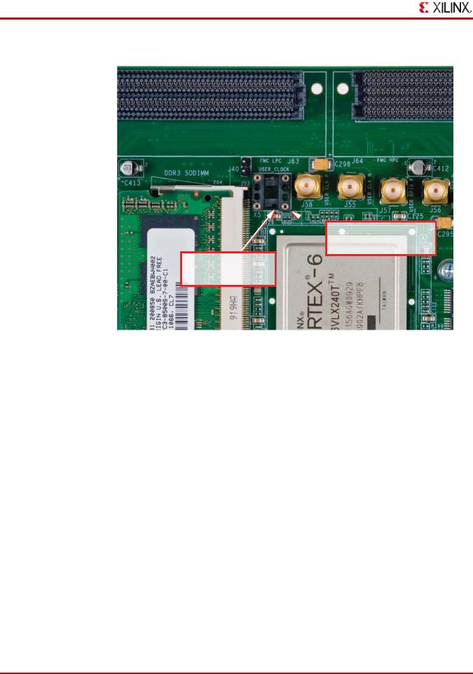
Chapter 1: ML605 Evaluation Board
 Silkscreened outline
has beveled corner
Socket has notch in crossbar
UG534_07_092109
Figure 1-7: ML605 Oscillator Socket Pin 1 Location Identifiers
28 |
www.xilinx.com |
ML605 Hardware User Guide |
|
|
UG534 (v1.2.1) January 21, 2010 |
Loading...