


Zetex ZXRD100ANQ16TA, ZXRD100ANQ16TC, ZXRD100APQ16TA, ZXRD100APQ16TC, ZXRD1033NQ16TA Datasheet
...ZXRD1000 SERIES
HIGH EFFICIENCY SIMPLESYNC PWM DC-DC CONTROLLERS
DESCRIPTION
The ZXRD1000 series provides complete control and protection functions for a high efficiency (> 95%) DC-DC converter solution. The choice of external MOSFETs allow the designer to size devices according to application. The ZXRD1000 series uses advanced DC-DC converter techniques to provide synchronous drive capability, using innovative circuits that allow easy and cost effective implementation of shoot through protection. The
FEATURES
•> 95% Efficiency
•Fixed frequency (adjustable) PWM
•Voltage mode to ensure excellent stability & transient response
•Low quiescent current in shutdown mode,15 A
•Low battery flag
•Output down to 2.0V
•Overload protection
•Demonstration boards available
•Synchronous or non-synchronous operation
•Cost effective solution
•N or P channel MOSFETs
•QSOP16 package
Very high efficiency SimpleSyncTM converter.
VCC
4.5-10V
ZXRD1000 series can be used with an all N channel topology or a combination N & P channel topology. Additional functionality includes shutdown control, a user adjustable low battery flag and simple adjustment of the fixed PWM switching frequency. The controller is available with fixed outputs of 5V or 3.3V and an adjustable (2.0 to 12V) output.
•Fixed 3.3, 5V and adjustable outputs
•Programmable soft start
APPLICATIONS
•High efficiency 5 to 3.3V converters up to 4A
•Sub-notebook computers
•Embedded processor power supply
•Distributed power supply
•Portable instruments
•Local on card conversion
•GPS systems
|
|
|
|
|
|
|
|
|
|
|
|
|
|
|
D2 |
|
|
|
|
|
|
|
|
|
|
|
|
|
|
|
|
|
|
|
|
BAT54 |
|
|
|
|
|
|
|
R1 |
|
|
IC1 |
13 |
|
|
|
|
|
|
|
ZXM64N02X |
|
|
|
|
|
|
|
|
100k |
|
|
|
|
VIN |
|
|
|
|
|
|
|
|
|
|
|
|
|
|
|
|
|
|
|
|
|
|
|
|
C10 |
|
N1 |
|
|
|
|
|
||
|
|
|
|
9 |
SHDN |
VDRIVE |
2 |
|
|
|
|
L1 |
|
|
|
|
||||
Shut Down |
|
|
|
|
|
|
1µF |
|
|
|
|
VOUT |
|
|||||||
|
|
|
|
|
|
|
|
|
|
|
|
|
|
15µH |
|
|
|
|||
|
|
|
C5 |
|
|
|
Bootstrap 1 |
|
|
|
|
|
|
C11 |
RSENSE |
|
|
3.3V 4A |
|
|
|
|
|
|
LBSET |
|
|
|
|
|
|
|
|
|
|
|
|||||
|
|
|
|
|
|
|
|
|
|
1µF |
0.01R |
|
|
|
|
|||||
|
|
|
1µF |
|
|
|
|
|
|
|
|
|
|
|
|
|
|
|
||
|
|
|
|
|
|
|
|
|
|
|
|
|
|
|
|
|
|
|
||
Low input flag |
|
|
|
11 LBF |
RSENSE+ |
7 |
C6 |
|
|
|
|
|
|
|
R6 |
Cx2 |
|
|
||
|
|
|
|
|
|
|
|
|
|
|
|
|
|
|
|
10k |
|
|
|
|
|
|
|
|
14 |
|
|
|
8 |
1µF |
|
|
|
|
|
|
|
0.01µF |
|
|
|
|
|
|
|
Delay |
RSENSE - |
|
|
|
|
|
|
|
|
|
|
|||||
|
|
|
|
10 |
|
|
|
|
|
|
|
|
|
|
|
|
|
|||
|
|
|
|
6 |
Decoup |
VFB |
16 |
|
|
|
|
|
|
|
|
|
|
COUT |
C9 |
|
|
|
|
|
5 |
VINT |
|
|
|
|
|
|
|
|
|
|
|
|
1µF |
||
|
|
|
|
C |
T |
Comp |
15 |
|
CX1 |
|
RX |
|
Fx |
C8 |
|
x2 |
|
|||
|
|
|
|
|
|
PWR |
R2 |
|
|
|
120µF |
|
||||||||
|
|
|
|
|
|
GND |
GND |
|
|
0.022µF |
2k7 |
|
D1 |
2.2µF |
R5 |
680µF |
|
|||
|
|
|
|
|
|
|
680R |
|
|
|
|
|
||||||||
CIN |
C1 |
C2 |
330pF |
1µF |
|
4 |
3 |
|
|
|
|
|
R4 |
D3 |
|
|
6k |
|
|
|
68µF |
|
|
|
|
|
|
|
|
10k |
|
ZHCS1000 |
|
|
|
|
|||||
|
|
|
C4 |
|
|
|
|
|
|
|
|
|
BAT54 |
N2 |
|
|
|
|
||
|
1µF |
1µF |
C3 |
|
|
|
C7 |
|
|
|
|
|
|
|
|
|
||||
|
|
|
|
|
|
|
|
|
|
|
|
|
|
|
|
|||||
|
|
|
|
|
|
|
|
|
|
ZXM64N02X |
|
|
|
|
|
|||||
|
|
|
|
|
|
|
22µF |
|
|
|
|
|
|
|
|
|
|
|||
|
|
|
|
|
|
|
|
|
|
|
|
|
|
|
|
|
|
|
||
|
|
|
|
|
R3 |
|
|
|
|
|
|
|
|
|
|
|
|
|
|
|
|
|
|
|
|
3k |
|
|
|
|
|
|
|
|
|
|
|
|
|
|
|
ISSUE 4 - OCTOBER 2000 |
1 |

ZXRD1000 SERIES
ABSOLUTE MAXIMUM RATINGS
Input without bootstrap (P suffix) |
20V |
RSENSE+, RSENSE - |
VIN |
|
Input with bootstrap(N suffix) |
10V |
Power dissipation |
610mW (Note 4) |
|
Bootstrap voltage |
20V |
|
Operating temperature |
-40 to +85°C |
Shutdown pin |
VIN |
|
Storage temperature |
-55 to +125°C |
LBSET pin |
VIN |
|
|
|
ELECTRICAL CHARACTERISTICS
TEST CONDITIONS (Unless otherwise stated) Tamb=25°C
Symbol |
Parameter |
Conditions |
Min |
Typ |
Max |
Unit |
|
|
|
|
|
|
|
VIN(min) |
Min. Operating Voltage |
No Output Device |
4.5 |
|
|
V |
VFB |
Feedback Voltage |
VIN=5V,IFB=1mA |
1.215 |
1.24 |
1.265 |
V |
(Note 1) |
|
|
|
|
|
|
|
4.5<VIN<18V |
1.213 |
1.24 |
1.267 |
V |
|
|
|
|||||
|
|
50 A<IFB<1mA,VIN=5V |
1.215 |
1.24 |
1.265 |
V |
TDRIVE |
Gate Output Drive Capability |
CG=2200pF(Note 2) |
|
60 |
|
ns |
|
|
CG=1000pF |
|
35 |
|
ns |
|
|
VIN=4.5V to maximim |
|
|
|
|
|
|
supply (Note 3) |
|
|
|
|
ICC |
Supply Current |
VIN=5V |
|
16 |
20 |
mA |
|
Shutdown Current |
VSHDN = 0V;VIN=5V |
|
15 |
50 |
A |
fosc |
Operating frequency range |
C3=1300pF |
50 |
50 |
300 |
kHz |
(Note 5) |
Frequency with timing capacitor |
|
|
|
||
|
|
C3=330pF |
|
200 |
|
|
fosc(tol) |
Oscillator Tol. |
|
|
|
± 25 |
% |
DC MAX |
Max Duty Cycle |
N Channel |
15 |
|
94 |
% |
|
|
P Channel |
0 |
|
100 |
% |
VRSENSE |
RSENSE voltage differential |
-40 to +85°C |
|
50 |
|
mV |
VCMRSENSE |
Common mode range of VRSENSE |
-40 to +85°C |
2 |
|
VIN |
V |
LBFSET |
Low Battery Flag set voltage |
|
1.5 |
|
VIN |
V |
LBFOUT |
Low Battery Flag output |
Active Low |
|
0.2 |
0.4 |
V |
LBFHYST |
Low Battery Flag Hysteresis |
|
10 |
20 |
50 |
mV |
LBFSINK |
Low Battery Flag Sink Current |
-40 to +85°C |
|
|
2 |
mA |
VSHDN |
Shutdown Threshold Voltage |
Low(off) |
1.5 |
|
0.25 |
V |
|
|
High(on) |
|
|
V |
|
ISHDN |
Shutdown Pin Source Current |
|
|
10 |
|
A |
Note 1. VFB has a different function between fixed and adjustable controller options. Note 2. 2200pF is the maximum recommended gate capacitance.
Note 3. Maximum supply for P phase controllers is 18V,maximum supply for N phase controllers is 10V. Note 4. See VIN derating graph in Typical Characteristics.
Note 5. The maximum frequency in this application is 300kHz. For higher frequency operation contact Zetex Applications Department.
2 |
ISSUE 4 - OCTOBER 2000 |

ZXRD1000 SERIES
TYPICAL CHARACTERISTICS
|
202 |
|
|
|
|
|
|
C3=330pF |
|
|
|
|
|
|
|
|
VIN=5V |
|
|
|
|
|
|
|
|
|
|
|
210 |
|
|
|
|
|
|
||
|
|
|
|
|
|
|
|
|
|
|
|
|
|
|
|
C3=330pF |
|
|
|
201 |
|
|
|
|
|
|
|
|
|
|
|
|
|
|
|
|
|
|
|
|
|
|
|
|
|
|
|
|
|
|
|
|
|
|
|
|
|
|
|
|
|
|
|
|
|
|
FOSC (kHz) |
205 |
|
|
|
|
|
|
|
OSC (kHz) |
200 |
|
|
|
|
|
|
|
|
|
|
|
|
|
|
|
|
|
199 |
|
|
|
|
|
|
|
|
200 |
|
|
|
|
|
|
|
||
|
|
|
|
|
|
|
|
|
|
|
|
|
|
|
|
|||
|
|
|
|
|
|
|
|
|
|
|
|
|
|
|
|
|
||
F |
|
|
|
|
|
|
|
|
|
|
195 |
|
|
|
|
|
|
|
|
|
|
|
|
|
|
|
|
|
|
|
|
|
|
|
|
|
|
|
198 |
|
|
|
|
|
|
|
|
|
|
|
|
|
|
|
|
|
|
|
|
|
|
|
|
|
|
|
|
190 |
|
|
|
|
|
|
|
|
197 |
|
|
|
|
|
|
|
|
|
|
|
|
|
|
|
|
|
|
4 |
6 |
8 |
10 |
12 |
14 |
16 |
18 |
20 |
|
-40 |
-20 |
0 |
20 |
40 |
60 |
80 |
100 |
VIN (V) |
Temperature (°C) |
FOSC v VIN |
FOSC v Temperature |
|
1.244 |
|
|
|
|
|
VOUT=3.3V |
|
1.25 |
|
|
|
|
|
|
|
|
|
|
|
|
|
|
|
|
|
VIN=5V |
|
|
|
|
|
|
||
|
|
|
|
|
|
|
|
|
|
|
|
|
|
|
|
|
|
|
|
|
|
|
|
|
|
|
|
1.245 |
VOUT=3.3V |
|
|
|
|
|
|
|
1.242 |
|
|
|
|
|
|
|
|
|
|
|
|
|
|
|
|
VFB (V) |
1.24 |
|
|
|
|
|
|
|
|
1.24 |
|
|
|
|
|
|
|
|
|
|
|
|
|
|
|
|
FB(V) |
|
|
|
|
|
|
|
|
|
|
|
|
|
|
|
|
|
|
V |
|
|
|
|
|
|
|
|
1.238 |
|
|
|
|
|
|
|
|
1.235 |
|
|
|
|
|
|
|
|
1.236 |
|
|
|
|
|
|
|
|
1.23 |
|
|
|
|
|
|
|
|
4 |
6 |
8 |
10 |
12 |
14 |
16 |
18 |
20 |
-40 |
-20 |
0 |
20 |
40 |
60 |
80 |
100 |
|
|
|
VIN (V) |
|
|
|
|
|
|
Temperature (°C) |
|
|
|
|||
|
|
|
VFB v VIN |
|
|
|
|
|
|
VFB v Temperature |
|
|
||||
1.02 |
|
|
|
|
|
|
|
|
|
|
|
|
|
|
VIN=5V |
|
|
|
|
|
|
|
|
|
|
|
|
|
|
|
|
|
|
|
|
|
|
|
|
|
|
|
1.005 |
|
|
|
|
|
|
|
1.01 |
|
|
|
|
|
|
|
|
|
|
|
|
|
|
|
|
|
|
|
|
|
|
|
|
|
1.000 |
|
|
|
|
|
|
|
1.00 |
|
|
|
|
|
|
|
|
NormalisedSETLB |
|
|
|
|
|
|
|
NormalisedSETLB |
|
|
|
|
|
|
|
|
|
|
|
|
|
|
|
|
|
|
|
|
|
|
|
|
|
0.995 |
|
|
|
|
|
|
|
0.99 |
|
|
|
|
|
|
|
|
|
|
|
|
|
|
|
|
4 |
6 |
8 |
10 |
12 |
14 |
16 |
18 |
20 |
-40 |
-20 |
0 |
20 |
40 |
60 |
80 |
100 |
|
|
|
VIN (V) |
|
|
|
|
|
|
Temperature (°C) |
|
|
|
|||
Normalised LBSET v VIN |
Normalised LBSET v Temperature |
ISSUE 4 - OCTOBER 2000 |
3 |
ZXRD1000 SERIES |
|
|
|
|
|
|
|
|
|
|
|
|
|||||||
|
|
|
|
|
TYPICAL CHARACTERISTICS |
|
|
|
|
|
|
||||||||
(mA) |
30 |
|
|
|
|
|
|
|
|
(mA) |
30 |
|
|
|
|
|
|
|
|
25 |
|
|
|
|
|
|
|
|
25 |
|
|
|
|
|
|
|
|
||
Current |
|
|
|
|
|
|
|
|
Current |
|
|
|
|
|
|
|
|
||
20 |
|
|
|
|
|
|
|
|
20 |
|
|
|
|
|
|
|
|
||
Supply |
|
|
|
|
|
|
|
|
Supply |
|
|
|
|
|
|
|
|
||
15 |
|
|
|
|
|
|
|
|
15 |
|
|
|
|
|
|
|
|
||
|
|
|
|
|
|
|
|
|
|
|
|
|
|
|
|
|
|
||
|
10 |
|
|
|
|
|
|
|
|
|
10 |
|
|
|
|
|
|
|
|
|
4 |
6 |
8 |
10 |
12 |
14 |
16 |
18 |
20 |
|
4 |
6 |
8 |
10 |
12 |
14 |
16 |
18 |
20 |
VIN (V) |
VIN (V) |
Supply Current v VIN |
Supply Current v VIN |
N Phase Device |
P Phase Device |
|
|
|
5 |
|
|
|
|
|
|
|
Vin=5V |
4 |
|
|
|
|
|
300 |
|
(A) |
|
|
|
|
|
|
FOSC(kHz) |
|
CurrentLimit |
3 |
|
|
|
|
|
200 |
|
|
|
|
|
|
|
|
|
|
|
2 |
|
|
|
|
|
100 |
|
|
|
|
VIN=5V |
|
|
|
|
|
|
1 |
|
|
|
|
|
|
|
|
|
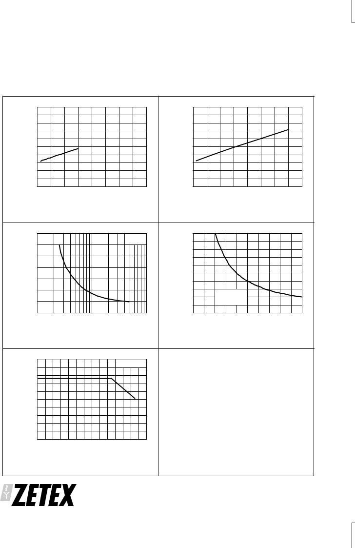
VOUT=3.3V |
|
|
|
|
|
|
|
|
|
|
|
|
|
0 |
|
|
0 |
|
|
|
|
|
100pF |
1nF |
10nF |
0 |
10 |
20 |
30 |
40 |
50 |
|
Timing Capacitance |
|
|
|
RSENSE (m ) |
|
|
|
FOSC v Capacitance |
Current Limit v RSENSE |
|
|
|
|
|
|
|
CG=2200pF |
|
|
20 |
|
|
|
|
|
|
|
VIN (V) |
15 |
|
|
|
|
|
|
|
10 |
|
|
|
|
|
|
|
|
|
5 |
|
|
|
|
|
|
|
|
-40 |
-20 |
0 |
20 |
40 |
60 |
80 |
100 |
Temperature (°C)
VIN Derating v Temperature
4 |
ISSUE 4 - OCTOBER 2000 |

DETAILED DESCRIPTION
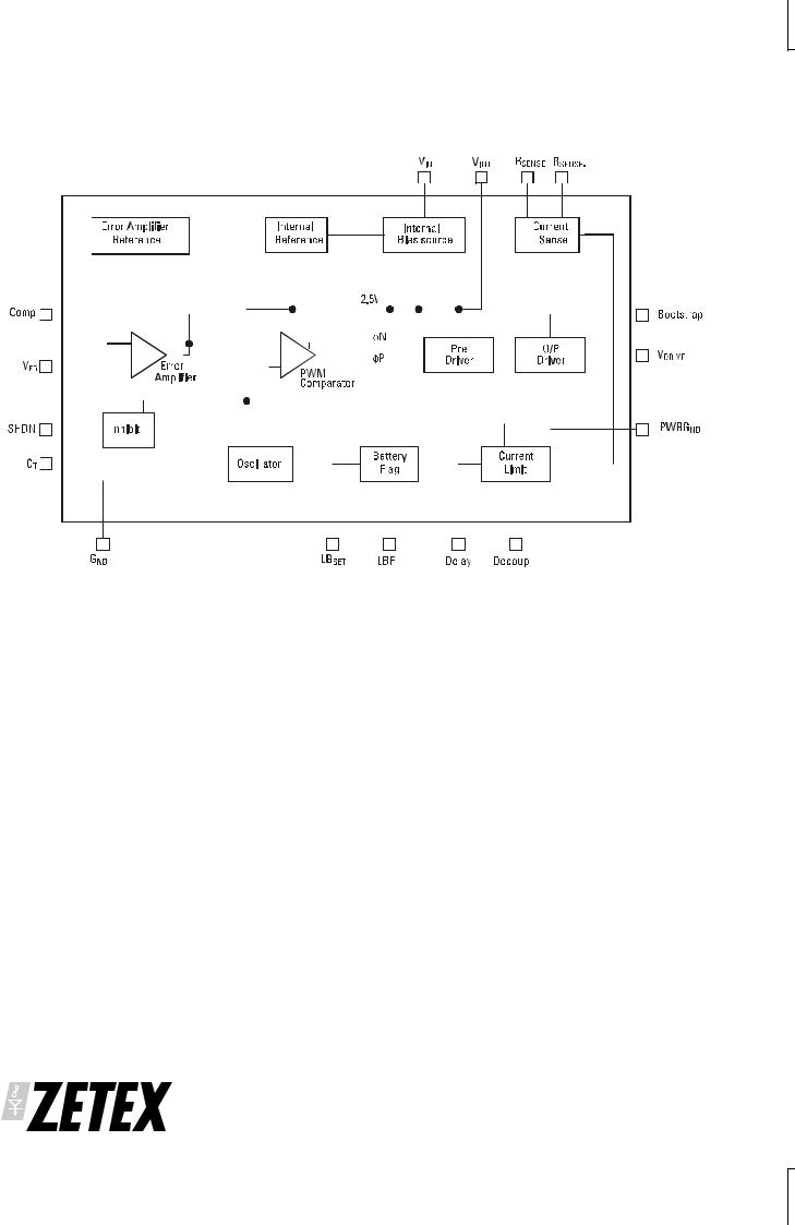
The ZXRD1000 series can be configured to use either N or P channel MOSFETs to suit most applications. The most popular format, an all N channel synchronous solution gives the optimum efficiency. A feature of the ZXRD1000 series solution is the unique method of generating the synchronous drive, called SimpleSync . Most solutions use an additional output from the controller, inverted and delayed from the main switch drive. The ZXRD1000 series solution uses a simple overwinding on the main choke (wound on the same core at no real cost penalty) plus a small ferrite bead . This means that the synchronous FET is only enhanced when the main FET is turned off. This reduces the ‘blanking period’ required for shootthrough protection, increasing efficiency and allowing smaller catch diodes to be used, making the controller simpler and less costly by avoiding complex timing circuitry. Included on chip are numerous functions that allow flexibility to suit most applications. The nominal switching frequency (200kHz) can be adjusted by a simple timing capacitor, C3. A low battery detect circuit is also provided. Off the shelf components are available from major manufacturers such as Sumida to provide either a single winding inductor for non-synchronous applications or a coil with an over-winding for synchronous applications. The combination of these switching characteristics, innovative circuit design and excellent user flexibility, make the ZXRD1000 series DC-DC solutions some of the smallest and most cost effective and electrically efficient currently available. Using Zetex’s HDMOS low RDS(on) devices, ZXM64N02X for the main and synchronous switch, efficiency can peak at upto 95% and remains high over a wide range of operating currents. Programmable soft start can also be adjusted via the capacitor, C7, in the compensation loop.
What is SimpleSyncTM?
Conventional Methods
In the conventional approach to the synchronous DC-DC solution, much care has to be taken with the timing constraints between the main and synchronous switching devices. Not only is this dependent upon individual MOSFET gate thresholds (which vary from device to device within data sheet limits and over temperature), but it is also somewhat dependent upon magnetics, layout and other parasitics. This normally means that significant ‘dead time’ has to be factored in to the design between the main and synchronous devices being turned off and on respectively. Incorrect application of dead time constraints can potentially lead to catastrophic short circuit conditions between VIN and GND. For some battery operated
ZXRD1000 SERIES
systems this can not only damage MOSFETs, but also the battery itself. To realise correct ‘dead time’ implementation takes complex circuitry and hence implies additional cost.
The ZETEX Method
Zetex has taken a different approach to solving these problems. By looking at the basic architecture of a synchronous converter, a novel approach using the main circuit inductor was developed. By taking the inverse waveform found at the input to the main inductor of a non - sy nchronous solution, a synchronous drive waveform can be generated that is always relative to the main drive waveform and inverted with a small delay. This waveform can be used to drive the synchronous switch which means no complex circuitry in the IC need be used to allow for shoot-through protection.
Implementation
Implementation was very easy and low cost. It simply meant peeling off a strand of the main inductor winding and isolating it to form a coupled secondary winding. These are available as standard items referred to in the applications circuits parts list.The use of a small, surface mount, inexpensive ’square loop’ ferrite bead provides an excellent method of eliminating shoot-through due to variation in gate thresholds. The bead essentially acts as a high impedance for the few nano seconds that shoot-through would normally occur. It saturates very quickly as the MOSFETs attain steady state operation, reducing the bead impedance to virtually zero.
Benefits
The net result is an innovative solution that gives a dditiona l bene fits whilst lowering overall implementation costs. It is also a technique that can be simply omitted to make a non-synchronous controller, saving further cost, at the expense of a few efficiency points.
ISSUE 4 - OCTOBER 2000 |
5 |
ZXRD1000 SERIES
Functional Block Diagram
|
|
|
|
|
|
|
|
|
|
|
|
|
|
|
|
|
|
|
|
|
|
|
|
|
|
|
|
|
|
|
|
|
|
|
|
|
|
|
|
|
|
|
|
|
|
|
|
|
|
|
|
|
|
|
|
|
|
|
|
|
|
|
|
|
|
|
|
|
|
|
|
|
|
|
|
|
|
|
|
|
|
|
|
|
|
|
|
|
|
|
|
|
|
|
|
|
|
|
|
|
|
|
|
|
|
|
|
|
|
|
|
|
|
|
|
|
|
|
|
|
|
|
|
|
|
|
|
|
|
|
|
|
|
|
|
|
|
|
|
|
|
|
|
|
|
|
|
|
|
|
|
|
|
|
|
|
|
|
|
|
|
|
|
|
|
|
|
|
|
|
|
|
|
|
|
|
|
|
|
|
|
|
|
|
|
|
|
|
|
|
|
|
|
|
|
|
|
|
|
|
|
|
|
|
|
|
|
|
|
|
|
|
|
|
|
|
|
|
|
|
|
|
|
|
|
|
|
|
|
|
|
|
|
|
|
|
|
|
|
|
|
|
|
|
|
|
|
|
|
|
|
|
|
|
|
|
|
|
|
|
|
|
|
|
|
|
|
|
|
|
|
|
|
|
|
|
|
|
|
|
|
|
|
|
|
|
|
|
|
|
|
|
|
|
|
|
|
|
|
|
|
|
|
|
|
|
|
|
|
|
|
|
|
|
|
|
|
|
|
|
|
|
|
|
|
|
|
|
|
|
|
|
|
|
|
|
|
|
|
|
|
|
|
|
|
|
|
|
|
|
|
|
|
|
|
|
|
|
|
|
|
|
|
|
|
|
|
|
|
|
|
|
|
|
|
|
|
|
|
|
|
|
|
|
|
|
|
|
|
|
|
|
|
|
|
|
|
|
|
|
|
|
|
|
|
|
|
|
|
|
|
|
|
|
|
|
|
|
|
|
|
|
|
|
|
|
|
|
|
|
|
|
|
|
|
|
|
|
|
|
|
|
|
|
|
|
|
|
|
|
|
|
|
|
|
|
|
|
|
|
|
|
|
|
|
|
|
|
|
|
|
|
|
|
|
|
|
|
|
|
|
|
|
|
|
|
|
|
|
|
|
|
|
|
|
|
|
|
|
|
|
|
|
|
|
|
|
|
|
|
|
|
|
|
|
|
|
|
|
|
|
|
|
|
|
|
|
|
|
|
|
|
|
|
|
|
|
|
|
|
|
|
|
|
|
|
|
|
|
|
|
|
|
|
|
|
|
|
|
|
|
|
|
|
|
|
|
|
|
|
|
|
|
|
|
|
|
|
|
|
|
|
|
|
|
|
|
|
|
|
|
|
|
|
|
|
|
|
|
|
|
|
|
|
|
|
|
|
|
|
|
|
|
|
|
|
|
|
|
|
|
|
|
|
|
|
|
|
|
|
|
|
|
|
|
|
|
|
|
|
|
|
|
|
|
|
|
|
|
|
|
|
|
|
|
|
|
|
|
|
|
|
|
|
|
|
|
|
|
|
|
|
|
|
|
|
|
|
|
|
|
|
|
|
|
|
|
|
|
|
|
|
|
|
|
|
|
|
|
|
|
|
|
|
|
|
|
|
|
|
|
|
|
|
|
|
|
|
|
|
|
|
|
|
|
|
|
|
|
|
|
|
|
|
|
|
|
|
|
|
|
|
|
|
|
|
|
|
|
|
|
|
|
|
|
|
|
|
|
|
|
|
|
|
|
|
|
|
|
|
|
|
|
|
|
|
|
|
|
|
|
|
|
|
|
|
|
|
|
|
|
PIN DESCRIPTIONS |
|
|
|
|
|
|
|
|
|
|
|
|
|
|
|
|
‡ See relevant Applications Section |
||||||||||||||||||||||||||
|
|
|
|
|
|
|
|
|
|
|
|
|
|
|
|
|
|
|
|
|
|
|
|
|
|
|
|
|
|
|
|
|
|
|
|
|
|
|
|
|
|
|
|
Pin No. |
Name |
Description |
|||||||||||||||||||||||||||||||||||||||||
|
|
|
|
|
|
|
|
|
|
|
|
|
|
|
|
|
|
|
|
|
|
|
|
|
|
|
|
|
|
|
|
|
|
|
|
|
|
|
|
|
|
|
|
1 |
|
|
|
Bootstrap |
Bootstrap circuit for generating gate drive |
||||||||||||||||||||||||||||||||||||||
|
|
|
|
|
|
|
|
|
|
|
|
|
|
|
|
|
|
|
|
|
|
|
|
|
|
|
|
|
|
|
|
|
|
|
|
|
|
|
|
|
|
|
|
2 |
|
|
|
VDRIVE |
Output to the gate drive circuit for main N/P channel switches |
||||||||||||||||||||||||||||||||||||||
3 |
|
|
|
PWRGND |
Power ground |
||||||||||||||||||||||||||||||||||||||
4 |
|
|
|
GND |
Signal ground |
||||||||||||||||||||||||||||||||||||||
5 |
|
|
|
CT |
Timing Capacitor sets oscillator frequency. ‡ |
||||||||||||||||||||||||||||||||||||||
6 |
|
|
|
VINT |
Internal Bias Circuit. Decouple with 1 F ceramic capacitor |
||||||||||||||||||||||||||||||||||||||
7 |
|
|
|
RSENSE+ |
Higher potential input to the current sense for current limit circuit |
||||||||||||||||||||||||||||||||||||||
8 |
|
|
|
RSENSE- |
Lower potential input to the current sense for current limit circuit |
||||||||||||||||||||||||||||||||||||||
9 |
|
|
|
|
|
|
|
|
|
|
|
|
|
Shutdown control. Active low. |
|||||||||||||||||||||||||||||
SHDN |
|||||||||||||||||||||||||||||||||||||||||||
|
|
|
|
|
|
|
|
|
|
|
|
|
|
|
|
|
|
|
|
|
|
|
|
|
|
|
|
|
|
|
|
|
|
|
|
|
|
|
|
|
|
|
|
10 |
|
|
|
Decoup |
Optional short circuit and overload decoupling capacitor for increased accuracy |
||||||||||||||||||||||||||||||||||||||
|
|
|
|
|
|
|
|
|
|
|
|
|
|
|
|
|
|
|
|
|
|
|
|
|
|
|
|
|
|
|
|
|
|
|
|
|
|
|
|
|
|
|
|
11 |
|
|
|
|
|
|
|
|
|
|
|
|
Low battery flag output. Active low, open collector output |
||||||||||||||||||||||||||||||
LBF |
|||||||||||||||||||||||||||||||||||||||||||
12 |
|
|
|
LBSET |
Low battery flag set. Can be connected to VIN if unused, or threshold set |
||||||||||||||||||||||||||||||||||||||
|
|
|
|
|
|
|
|
|
|
|
|
|
|
|
via potential divider. ‡ |
||||||||||||||||||||||||||||
13 |
|
|
|
VIN |
Input Voltage |
||||||||||||||||||||||||||||||||||||||
14 |
|
|
|
|
Delay |
External R and C to set the desired cycle time for hiccup circuit. ‡ |
|||||||||||||||||||||||||||||||||||||
|
|
|
|
|
|
|
|
|
|
|
|
|
|
|
|
|
|
|
|
|
|
|
|
|
|
|
|
|
|
|
|
|
|
|
|
|
|
|
|
|
|
|
|
15 |
|
|
|
Comp |
Compensation pin to allow for stability components and soft start. ‡ |
||||||||||||||||||||||||||||||||||||||
|
|
|
|
|
|
|
|
|
|
|
|
|
|
|
|
|
|
|
|
|
|
|
|
|
|
|
|
|
|
|
|
|
|
|
|
|
|
|
|
|
|
|
|
16 |
|
|
|
VFB |
Feedback Voltage. This pin has a different function between fixed and |
||||||||||||||||||||||||||||||||||||||
|
|
|
|
|
|
|
|
|
|
|
|
|
|
|
adjustable controller options. The appropriate controller must be used for |
||||||||||||||||||||||||||||
|
|
|
|
|
|
|
|
|
|
|
|
|
|
|
the fixed or adjustable solution. Connect to VOUT for fixed output, or to |
||||||||||||||||||||||||||||
|
|
|
|
|
|
|
|
|
|
|
|
|
|
|
potential divider for adjustable output. ‡ |
||||||||||||||||||||||||||||
6 |
ISSUE 4 - OCTOBER 2000 |

Applications
Note: Component names refer to designators shown in the application circuit diagrams.
Output Capacitors
Output capacitors are a critical choice in the overall performance of the solution. They are required to filter the output and supply load transient current. They are also affected by the switching frequency, ripple current, di/dt and magnitude of transient load current. ESR plays a key role in determining the value of capacitor to be used. Combination of both high frequency, low value ceramic capacitors and low ESR bulk storage capacitors optimised for switching applications provide the best response to load transients and ripple requirements. Electrolytic capacitors with low ESR are larger and more expensive so the ultimate choice is always a compromise between size, cost and performance. Care must also be taken to ensure that for large capacitors, the ESL of the leads does not become an issue. Excellent low ESR tantalum or electrolytic capacitors are available from Sanyo OS-CON, AVX, Sprague and Nichicon.
The output capacitor will also affect loop stability, transient performance. The capacitor ESR should preferably be of a similar value to the sense resistor. Parallel devices may be required.
IRIPPLE(RMS) = |
0.29 VOUT (VIN−VOUT) |
|
L f VIN |
||
|
where L= output filter inductance f= switching frequency
For output voltage ripple it is necessary to know the peak ripple current which is given by:
Ipk−pk = VOUT( VIN− VOUT)
L f VIN
Voltage ripple is then:-
VRIPPLE = Ipk − pk ESR
ZXRD1000 SERIES
Input Capacitors
The input capacitor is chosen for its RMS current and voltage rating. The use of low ESR electrolytic or tantalum capacitors is recommended. Tantalum capacitors should have their voltage rating at 2VIN (max), electrolytic at 1.4VIN(max). IRMS can be approximated by:
IRMS = IOUT √(VOUT(VIN−VOUT) )
VIN
Underspecification of this parameter can affect long term reliability. An additonal ceramic capacitor should be used to provide high frequency decoupling at VIN.
Also note that the input capacitance ESR is effectively in series with the input and hence contributes to efficiency losses related to IRMS2 * ESR of the input capacitor.
MOSFET Selection
The ZXRD1000 family can be configured in circuits where either N or P channel MOSFETs are employed as the main switch. If an N channel device is used, the corresponding N phase controller must be chosen. Similarly, for P channel main switch a P phase controller must be used. The ordering information has a clear identifier to distinguish between N and P phase controllers.
The MOSFET selection is subject to thermal and gate drive considerations. Care also has to be taken to allow for transition losses at high input voltages as well as RDS(ON) losses for the main MOSFET . It is recommended that a device with a drain source breakdown of at least 1.2 times the maximum VIN should be used.
For optimum efficiency , two N channel low RDS(on) devices are required. MOSFETs should be selected with the lowest RDS(ON) consistent with the output current required. As a guide, for 3-4A output, <50mΩ devices would be optimum, provided the devices are low gate threshold and low gate charge. Typically look for devices that will be fully enhanced with 2.7V VGS for 4-5A capability.
Zetex offers a range of low RDS(ON)logic level MOSFETs which are specifically designed with DC-DC power conversion in mind. Packaging includes SOT23, SOT23-6 and MSOP8 options. Ideal examples of optimum devices would be Zetex ZXM64N03X and ZXM64N02X (N channel). Contact your local Zetex office or Zetex web page for further information.
ISSUE 4 - OCTOBER 2000 |
7 |
ZXRD1000 SERIES
Applications (continued)
Inductor Selection
The inductor is one of the most critical components in the DC-DC circuit.There are numerous types of devices available from many suppliers. Zetex has opted to specify off the shelf encapsulated surface mount components, as these represent the best compromise in terms of cost, size, performance and shielding.
The SimpleSyncTM technique uses a main inductor with an overwinding for the gate drive which is available as a standard part. However, for engineers who wish to design their own custom magnetics, this is a relatively simple and low cost construction technique. It is simply formed by terminating one of the multiple strands of litz type wire separately. It is still wound on the same core as the main winding and only has to handle enough current to charge the gate of the synchronous MOSFET. The major benefit is circuit simplification and hence lower cost of the control IC. For non-synchronous operation, the overwinding is not required.
The choice of core type also plays a key role. For optimum performance, a ’swinging choke’ is often preferred. This is one which exhibits an increase in inductance as load current decreases. This has the net effect of reducing circulating current at lighter load improving efficiency. There is normally a cost premium for this added benefit. For this reason the chokes specified are the more usual constant inductance type.
Peak current of the inductor should be rated to minimum 1.2IOUT (max) . To maximise efficiency, the winding resistance of the main inductor should be less than the main switch output on resistance.
Schottky Diode
Selection depends on whether a synchronous or non-synchronous approach is taken. For the ZXRD1000, the unique approach to the synchronous drive means minimal dead time and hence a small SOT23 1A DC rated device will suffice, such as the ZHCS1000 from Zetex. The device is only designed to prevent the body diode of the synchronous MOSFET from conducting during the initial switching transient until the MOSFET takes over. The device should be connected as close as possible to the source terminals of the main MOSFET.
For non-synchronous applications , the Schottky diode must be selected to allow for the worst case
conditions, when VIN is at its highest and VOUT is lowest (short circuit conditions for example). Under these conditions the device must handle peak current at close to 100% duty cycle.
Frequency Adjustment
The nominal running frequency of the controller is set to 200kHz in the applications shown. This can be adjusted over the range 50kHz to 300kHz by changing the value of capacitor on the CT pin. A low cost ceramic capacitor can be used.
Frequency = 60000/C3 (pF)
Frequency v temperature is given in the typical characteristics.
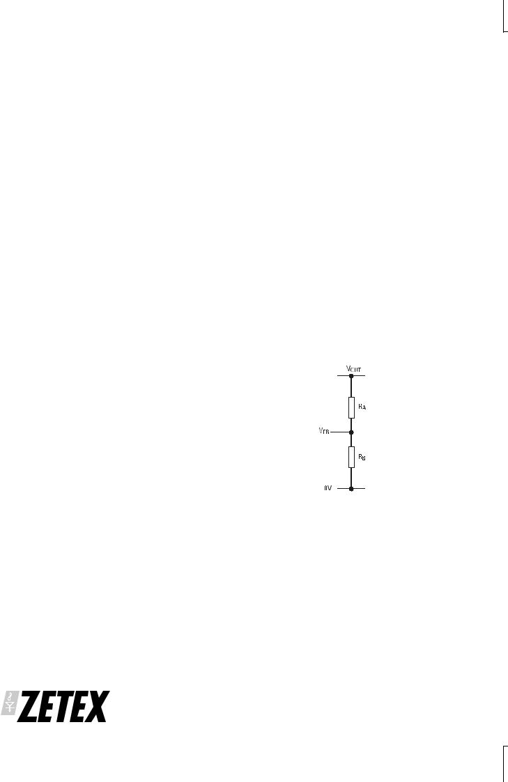
Output Voltage Adjustment
The ZXRD1000 is available as either a fixed 5V, 3.3V or adjustable output. On fixed output versions, the VFB pin should be connected to the output. Adjustable operation requires a resistive divider connected as follows:
The value of the output voltage is determined by the equation
VOUT = VFB ( 1 + |
RA |
) VFB = 1.24V |
|
||
|
RB |
|
Note: The adjustable circuit is shown in the following transient optimisation section. It is also used in the evaluation PCB. In both these circuits RA is assigned the label R6 and RB the label R5.
Values of resistor should be between 1k and 20k to guarantee operation. Output voltage can be adjusted in the range 2V to 12V for non-synchronous applications. For synchronous applications, the minimum VOUT is set by the VGS threshold required for the synchronous MOSFET, as the swing in the gate using the SimpleSyncTM technique is approximately VOUT.
8 |
ISSUE 4 - OCTOBER 2000 |
ZXRD1000 SERIES
Applications (continued)
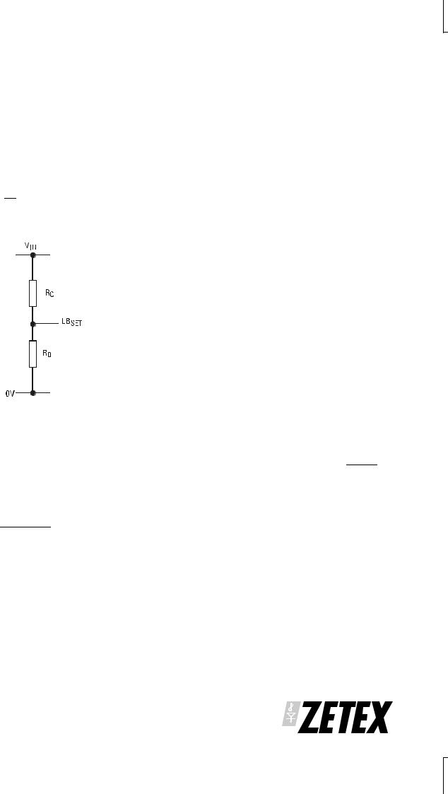
Low Battery Flag
The low battery flag threshold can be set by the user to trip at a level determined by the equation:
VLBSET = 1.25 ( 1 + RC )
RD
RD is recommended to be 10k where RC and RD are connected as follows:
Hiccup Time Constant
The hiccup circuit (at the ’delay’ pin) provides overload protection for the solution. The threshold of the hiccup mode is determined by the value of RSENSE, When >50mV is developed across the sense resistor, the hiccup circuit is triggered, inhibiting the device.
It will stay in this state depending upon the time constant of the resistor and capacitor connected at the ’delay’ pin. In order to keep the dissipation down under overload conditions it is recommended the circuit be off for approximately 100ms. If for other application reasons this is too long an off period, this can be reduced at least by 10:1, care needs to be taken that any increased dissipation in the external MOSFET is still acceptable. The resistor capacitor combination R1,C1 recommended in the applications circuits provides a delay of 100ms.
Hysteresis is typically 20mV at the LBSET pin.
Current Limit
A current limit is set by the low value resistor in the output path, RSENSE. Since the resistor is only used for overload current limit, it does not need to be accurate and can hence be a low cost device.
The value of the current limit is set by using the equation:
50(mV)
ILIM (A) = RSENSE(mΩ )
A graph of Current Limit v RSENSE is shown in the typical characteristics. This should assist in the selection of RSENSE appropriate to application.
If desired, RSENSE can also be on the input supply side.
When used on the input side RSENSE should be in series with the upper output device (i.e. in series with the drain or source in N and P channel solutions respectively).Typically in this configuration RSENSE will be 20m .
Soft Start & Loop Stability
Soft start is determined by the time constant of the capacitor and resistor C7 and R3. Typically a good starting point is C7 = 22µ F and R3 = 24k for fixed voltage variants. For fully adjustable variants see Optimising for Transient Response later in the applications section. This network also helps provide good loop stability.
Low Quiescent Shutdown
Shutdown control is provided via the SHDN pin, putting the device in to a low quiescent sleep mode. In some circumstances where rapid sequencing of VCC can occur (when VCC is turned off and back on) and VCC has a very rapid rise time (100-200ms) timing conflicts can occur.
ISSUE 4 - OCTOBER 2000 |
9 |
 Loading...