

Page 1
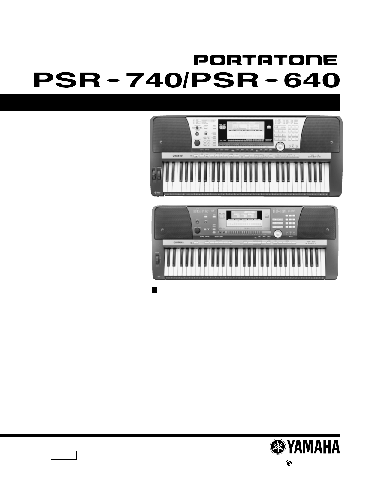
SERVICE MANUAL
PSR-740
PSR-640
001627
PK
PSR-740 19990901-160000
PSR-640 19990901-120000
CONTENTS
SPECIFICATIONS .............................................. 3/4
PANEL LAYOUT ...................................... 5
PSR-740 BLOCK DIAGRAM
PSR-640 BLOCK DIAGRAM
.... 6
.... 7
CIRCUIT BOARD LAYOUT ................. 8
DISASSEMBLY PROCEDURE ............................. 10
LSI PIN DESCRIPTION ............................... 14
IC BLOCK DIAGRAM .................................. 19
CIRCUIT BOARDS ........................................ 20
TEST PROGRAM ............................. 25/27
DATA INITIALIZATION .......................................... 29
ALERT MESSAGE LIST ................... 30/32
MIDI DATA FORMAT ................. 34
PSR-740 MIDI IMPLEMENTATION CHART ......................... 49
PSR-640 MIDI IMPLEMENTATION CHART ......................... 50
PARTS LIST
OVERALL CIRCUIT DIAGRAM
1.82K-9201 Printed in Japan ‘99.08
HAMAMATSU, JAPAN
Page 2
PSR-740/PSR-640
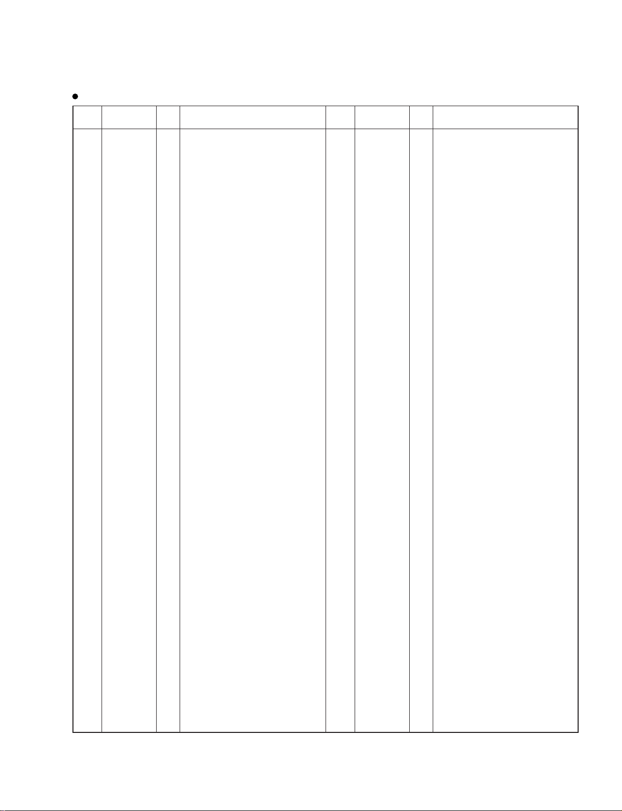
PSR-740 BLOCK DIAGRAM
PN
IC29
17-19 21
IC33
5
7
IC28
123 122
IC4
IC14 IC14
IC25
108
94,96
34
35
234
120
114
5
232
231
43
48
114
IC23
134
IC24
81
101
135
136
102,103
223,221
77
76,222,225
IC6
13
14
27
28
29
TA2 TA1
IC15
IC10
IC32
IC19 IC18 IC20
11 11
IC11 IC12 IC9
(1)
11 13 32
14 29 28 13 14 29 28 13
(1)
IC7 IC8
(2)
11 13 32
(2)
IC21
22 24 29
IC16
IC17 IC5
19 6
17
10 13 14 37
IC13
15
14
13
12
11
4
IC14
IC15
439
1 3 5 7 20 21 40
IC310
IC1
IC2
PC1
IC410
IC30
86,98,99
IC26
IC22
33
IC31
IC27
8
IC3 IC1
IC2
IC210,220
IC320
IC510
6
IC610
IC710
28CA1-8814457
Page 3
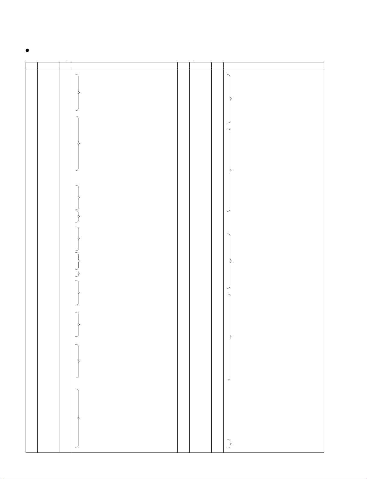
PSR-640 BLOCK DIAGRAM
PSR-740/PSR-640
IC190
108
194
196
122
IC100
43
48
53
114
TR501-505 IC530
IC510
(1)
11 13 32
IC500
IC420
19 6
IC430
11
11
IC410
IC400
17
10 13 14 37 1 3 5 7 20 21 40
IC800
IC1
439
IRQFD
PC1
IC350
4
15
14
13
12
11
IC360
(2)
11 13 32
IC330IC300IC320IC310
13 14 31 3022 24 29
28CA1-8813472
IC
IC210 12 74,73
220
IC260
11 6 10
43,44,101
IC200
150
151
152
158
159
163
164
IC360
IC370
9
IC290
IC600
IC610
IC410
IC900
IC310
IC210,220
25
IC610
IC320
IC510
IC610
IC710
7
Page 4
PSR-740/PSR-640
LSI PIN DESCRIPTION
SH-7043A (XW485100) CPU
SH-7043 (XW180100) CPU
PIN
NO.
NAME I/O FUNCTION
1 /WRHH/PA23 O HH write/Port A 73 D15 I/O
2 DACK0/PE14 O DMA transfer strobe/Port E 74 D14 I/O Data bus
3 /WRHL/PA22 O HL write/Port A 75 D13 I/O
4 /CASHH/PA21 I/O HH Column address strobe/Port A 76 D12 I/O
5 DACK1/PE15 O DMA transfer strobe/Port E 77 VCC I Power supply
6 VSS I Ground 78 D11 I/O Data bus
7 A0 O 79 VSS I Ground
8 A1 O 80 D10 I/O
9 A2 O Address bus 81 D9 I/O
10 A3 O 82 D8 I/O Data bus
11 A4 O 83 D7 I/O
12 VCC I Power supply 84 D6 I/O
13 A5 O Address bus 85 VCC I Power supply
14 VSS I Ground 86 D5 I/O Data bus
15 A6 O 87 VSS I Ground
16 A7 O 88 D4 I/O
17 A8 O 89 D3 I/O
18 A9 O 90 D2 I/O Data bus
19 A10 O 91 D1 I/O
20 A11 O Address bus 92 D0 I/O
21 A12 O 93 VSS I Ground
22 A13 O 94 XTAL I Crystal oscillator
23 A14 O 95 MD3 I Mode select
24 A15 O 96 EXTAL I Crystal oscillator
25 A16 O 97 MD2 I Mode select
26 VCC I Power supply 98 NMI - Non-maskable interrupt
27 A17 O Address bus 99 VCC/FW I Power supply
28 VSS I Ground 100 PA16 I/O Port A
29 /CASHL/PA20 I/O HL Column address strobe/Port A 101 PA17 I/O Port A
30 PA19 I/O Port A 102 MD1 I Mode select
31 /RAS/PB2 O Row address strobe/Port B 103 MD0 I Mode select
32 /CASL/PB3 O Column address strobe (low) /Port B 104 PLLVCC I PLL Power supply
33 PA18 I/O Port A 105 PLLCAP I PLL capacitor
34 /CASH/PB4 O Column address strobe (high) /Port B 106 PLLVSS I PLL Ground
35 VSS I Ground 107 CK/PA15 I/O Clock/Port A
36 RDWR/PB5 O DRAM read/write /Port B 108 /RES I Reset
37 A18 O 109 DREQ0/PE0 I/O DMA transfer request/Port E
38 A19 O Address bus 110 TIOC0B/PE1 I/O MTU input capture/output compare (ch 0)/Port E
39 A20 O 111 /DREQ1/PE2 I/O DMA transfer request/Port E
40 VCC I Power supply 112 VCC I Power supply
41 A21 O Address bus 113 PE3 I/O
42 VSS I Ground 114 PE4 I/O Port E
43 /RD O Read 115 PE5 I/O
44 /WDTOVF O Watch dog timer overflow 116 PE6 I/O
45 D31 I/O Data bus 117 VSS I Ground
46 D30 I/O Data bus 118 AN0 /PF0 I
47 /WRH O High write 119 AN1/ PF1 I
48 /WRL O Low write 120 AN2 /PF2 I
49 /CS1 O Chip select 121 AN3 /PF3 I Analog input/Port F
50 /CS0 O Chip select 122 AN4 /PF4 I
51 /IRQ3/PA9/TCLKD I/O Interrupt request/Port A/clock 123 AN5/PF5 I
52 /IRQ2/PA8/TCKLC I/O Interrupt request/Port A/clock 124 AVSS I Analog ground
53 /CS3 O Chip select 125 AN6/PF6 I Analog input/ Port F
54 /CS2 O Chip select 126 AN7/PF7 I Analog input /Port F
55 VSS I Ground 127 AVREF I Analog reference voltage
56 D29 I/O 128 AVCC I Analog power supply
57 D28 I/O 129 VSS I Ground
58 D27 I/O Data bus 130 RxDO I Receive data
59 D26 I/O 131 TxDO O Transmit data
60 D25 I/O 132 /IRQ0/SCK0 I Interrupt request/Serial clock
61 VSS I Ground 133 RxD1 I Receive data
62 D24 I/O Data bus 134 TxD1/PA4 I/O SCI/Port A
63 VCC I Power supply 135 VCC I Power supply
64 D23 I/O 136 /IRQ1/SCK1 I Interrupt request/Serial clock
65 D22 I/O 137 PE7 I/O
66 D21 I/O 138 PE8 I/O Port E
67 D20 I/O Data bus 139 PE9 I/O
68 D19 I/O 140 PE10 I/O
69 D18 I/O 141 VSS I Ground
70 D17 I/O 142 PE11 I/O
71 VSS I Ground 143 PE12 I/O Port E
72 D16 I/O Data bus 144 PE13 I/O
PIN
NO.
NAME I/O FUNCTION
14
Page 5
HG73C205AFD (XU947C00) SWX00B TONE GENERATOR
1 ICN I Initial clear 85 CMA3 O Program address bus
2 RFCLKI I PLL Clock 86 CMA8 O Program address bus
3 TM2 I PLL Control 87 CMA2 O Program address bus
4 AVDD_PLL Power supply 88 CRD O read signal
5 AVSS_PLL Ground 89 CMA1 O Program address bus
6 MODE0 I SWX dual mode 90 CUB O high byte effective signal
7 VCC7 Power supply 91 VCC91 Power supply
8 GND8 Ground 92 GHND92 Ground
9 XIN I crystal oscillator 93 CS1 O CS signal
10 XOUT O crystal oscillator 94 CMA0 O Program address bus
11 MODE1 I SWX separate mode 95 CLB O low byte effective signal
12 TEST0 I TEST pin 96 CMA12 O
13 TESTON I TEST pin 97 CMA11 O
Program address bus
14 AN0-P40 I A/D converter 98 CMA10 O
15 AN1-P41 I A/D converter 99 CMA9 O
16 AN2-P42 I A/D converter 100 GND100 Ground
17 AN3-P43 I A/D converter 101 CWE O write signal
18 AVDD_AN Power supply 102 CMA16 O Program address bus
19 AVSS_AN Ground 103 CMA15 O Program address bus
20 TXD0 O for MIDI or TO-HOST 104 CMA14 O Program address bus
21 TXD1 O for MIDI 105 CMA13 O Program address bus
22 EXCLK I Crystal oscillator 106 CMD8 I/O Program memory Data bus
23 SMD11 I/O Wave memory data bus 107 CMD7 I/O Program memory Data bus
24 SMD4 I/O Wave memory data bus 108 CMD9 I/O Program memory Data bus
25 SMD3 I/O Wave memory data bus 109 CMD6 I/O Program memory Data bus
26 SMD12 I/O Wave memory data bus 110 CMD10 I/O Program memory Data bus
27 SMD10 I/O Wave memory data bus 111 CMD5 I/O Program memory Data bus
28 SMD5 I/O Wave memory data bus 112 CMD11 I/O Program memory Data bus
29 SMD2 I/O Wave memory data bus 113 CMD4 I/O Program memory Data bus
30 SMD13 I/O Wave memory data bus 114 CMD12 I/O Program memory Data bus
31 SMD9 I/O Wave memory data bus 115 CMD3 I/O Program memory Data bus
32 SMD6 I/O Wave memory data bus 116 CMD13 I/O Program memory Data bus
33 SMD1 I/O Wave memory data bus 117 CMD2 I/O Program memory Data bus
34 SMD14 I/O Wave memory data bus 118 CMD14 I/O Program memory Data bus
35 VCC35 Power supply 119 VCC119 Power supply
36 GND36 Ground 120 GND115 Ground
37 SMD8 I/O Wave memory data bus 121 CMD1 I/O Program memory Data bus
38 SMD7 I/O Wave memory data bus 122 CMD15 I/O Program memory Data bus
39 SMD0 I/O Wave memory data bus 123 CMD0 I/O Program memory Data bus
40 SMD15 I/O Wave memory data bus 124 CMA21 O Program address bus
41 SOE O read signal 125 PDT15 I/O
42 SWE O write signal 126 PDT14 I/O
43 SRAS O RAS signal 127 PDT13 I/O
44 SCAS O CAS signal 128 PDT12 I/O
45 REFRESH O REFRESH signal 129 PDT11 I/O
SWX access data bus
46 CS0 O CS signal 130 PDT10 I/O
47 SMA0 O Memory address bus 131 PDT9 I/O
48 SMA16 O Memory address bus 132 PDT8 I/O
49 VCC49 Power supply 133 VCC133 Power supply
50 GND50 Ground 134 GND134 Ground
51 SMA1 O Memory address bus 135 PDT7 I/O
52 SMA15 O Memory address bus 136 PDT6 I/O
53 SMA2 O Memory address bus 137 PDT5 I/O
54 SMA14 O Memory address bus 138 PDT4 I/O
SWX access data bus
55 SMA3 O Memory address bus 139 PDT3 I/O
56 SMA13 O Memory address bus 140 PDT2 I/O
57 SMA4 O Memory address bus 141 PDT1 I/O
58 SMA12 O Memory address bus 142 PDT0 I/O
59 SMA5 O Memory address bus 143 VCA143 Power supply
60 GND60 Ground 144 GND144 Ground
61 VCC61 Power supply 145 PAD2 I
62 SMA11 O Memory address bus 146 PAD1 I SWX access address bus
63 SMA6 O Memory address bus 147 PAD0 I
64 SMA10 O Memory address bus 148 VCC148 Power supply
65 SMA7 O Memory address bus 149 GND149 Ground
66 SMA9 O Memory address bus 150 PCS I Chip select
67 SMA17 O Memory address bus 151 PWR I write enable
68 SMA8 O Memory address bus 152 PRD I read enable
69 SMA18 O Memory address bus 153 RXD0 I for Midi or TO-HOST
70 SMA19 O Memory address bus 154 RXD1 I for Midi or Key scan
71 SMA20 O Memory address bus 155 SCLKI I EXT Clock
72 SMA21 O Memory address bus 156 ADIN I A/D converter
73 SMA22 O Memory address bus 157 ADLR O A/D converter LR clock
74 SMA23 O Memory address bus 158 DO0 O DAC
75 CMA20 O Program address bus 159 DO1 O DAC
76 CMA19 O Program address bus 160 SYSCLK O 1/2 clock
77 VCC77 Power supply 161 VCC161 Power supply
78 GND78 O Ground 162 GND162 Ground
79 CMA18 O Program address bus 163 WCLK O for DAC LR clock
80 CMA17 O Program address bus 164 QCLK O 1/12 clock
81 CMA5 O Program address bus 165 BCLK O IIS-DAC clock
82 CMA6 O Program address bus 166 SYI I Synch signal
83 CMA4 O Program address bus 167 IRQ0 I Interrupt request
84 CMA7 O Program address bus 168 NMI I Interrupt request
PIN
NAME I/O FUNCTION
NO.
PIN
NAME I/O FUNCTION
NO.
PSR-740/PSR-640
15
Page 6
PSR-740/PSR-640
()
TC203C760HF-002 (XS725A00)
SWP30B (AWM Tone Generator coped with MEG) Standard Wave Processor
PIN
NAME
NO.
1
CA0
2
CA1
3
CA2
4
CA3
5
CA4
6
CA5
7
CA6
8
CA7
9
CA8
10
CA9
11
CA10
12
CA11
13
VSS
14
CD0
15
CD1
16
CD2
17
CD3
18
CD4
19
CD5
20
CD6
21
CD7
22
CD8
23
CD9
24
CD10
25
CD11
26
CD12
27
CD13
28
CD14
29
VDD
30
VSS
31
CD15
32
33
/WR
34
/RD
35
VDDS
36
SYSH0
37
SYSH1
38
SYSH2
39
SYSH3
40
SYSH4
41
SYSH5
42
SYSH6
43
SYSH7
44
KONO0
45
KONO1
46
KONO2
47
KONO3
48
VSS
49
SYSL0
50
SYSL1
51
SYSL2
52
SYSL3
53
SYSL4
54
SYSL5
55
SYSL6
56
SYSL7
57
KONI0
58
KONI1
59
VDDS
60
VSS
61
KONI2
62
KONI3
63
DAC0
64
DAC1
65
WCLK
66
MELO0
67
MELO1
68
MELO2
69
MELO3
70
MELO4
71
MELO5
72
MELO6
73
MELO7
74
VDDS
75
ADLR
76
MELI0
77
MELI1
78
MELI2
79
MELI3
80
MELI4
81
MELI5
82
MELI6
83
MELI7
84
VSS
85
/RCAS
86
RA8
87
RA7
88
RA6
89
VDD
90
VSS
91
RA5
92
RA4
93
RA3
94
RA2
95
RA1
96
RA0
97
/RRAS
98
/RWE
99
VSS
100
RD7
101
RD6
102
RD5
103
RD4
104
RD3
105
RD2
106
RD1
107
RD0
108
VSS
109
RD17
110
RD16
111
RD15
112
113
RD14
114
RD13
115
RD12
116
RD11
117
RD10
118
RD9
119
RD8
120
VDDS
Vss
/CS
I/O
I
I
I
I
I
I
I
I
I
I
I
I
I/O
I/O
I/O
I/O
I/O
I/O
I/O
I/O
I/O
I/O
I/O
I/O
I/O
I/O
I/O
I/O
I
I
I
O
O
O
O
O
O
O
O
O
O
O
O
I/O
I/O
I/O
I/O
I/O
I/O
I/O
I/O
I
I
I
I
I
O
O
O
O
O
O
O
O
O
O
O
O
I
I
I
I
I
I
I
I
O
O
O
O
O
O
O
O
O
O
O
O
I/O
I/O
I/O
I/O
I/O
I/O
I/O
I/O
I/O
I/O
I/O
I/O
I/O
I/O
I/O
I/O
I/O
I/O
Address bus internal register
Data bus of internal register
Chip select
Write strobe
Read strobe
NSYS/LNSYS upper 16 bits
Key on data
NSYS input/LNSYS output lower 8 bits
Key on data (Power supply)
DAC output
DAC0/DAC1 word clock
MEL wave data output
ADC word clock
MEL wave data input
DRAM column address strobe
DRAM address bus
DRAM row address strobe
DARM write enable
DRAM data bus
FUNCTION
(Ground)
(Ground)
(Power supply)
(Ground)
(Power supply)
(Ground)
(Ground)
(Power supply)
(Ground)
(Power supply)
(Ground)
(Ground)
(Ground)
(Power supply)
PIN
NO.
121
122
123
124
125
126
127
128
129
130
131
132
133
134
135
136
137
138
139
140
141
142
143
144
145
146
147
148
149
150
151
152
153
154
155
156
157
158
159
160
161
162
163
164
165
166
167
168
169
170
171
172
173
174
175
176
177
178
179
180
181
182
183
184
185
186
187
188
189
190
191
192
193
194
195
196
197
198
199
200
201
202
203
204
205
206
207
208
209
210
211
212
213
214
215
216
217
218
219
220
221
222
223
224
225
226
227
228
229
230
231
232
233
234
235
236
237
238
239
240
NAME
VSS
HMD0
HMD1
HMD2
HMD3
HMD4
HMD5
HMD6
HMD7
HMD8
HMD9
HMD10
HMD11
HMD12
HMD13
HMD14
HMD15
VSS
HMA0
HMA1
HMA2
HMA3
HMA4
HMA5
HMA6
HMA7
HMA8
HMA9
HMA10
VSS
VDD
HMA11
HMA12
HMA13
HMA14
HMA15
HMA16
HMA17
HMA18
HMA19
HMA20
HMA21
HMA22
HMA23
HMA24
VSS
/MRAS
/MCAS
/MOE
/MWE
VSS
LMD0
LMD1
LMD2
LMD3
LMD4
LMD5
LMD6
LMD7
VDDS
VSS
LMD8
LMD9
LMD10
LMD11
LMD12
LMD13
LMD14
LMD15
VSS
LMA0
LMA1
LMA2
LMA3
LMA4
LMA5
LMA6
LMA7
LMA8
LMA9
LMA10
LMA11
VSS
LMA12
LMA13
LMA14
LMA15
LMA16
LMA17
VDD
VSS
LMA18
LMA19
LMA20
LMA21
LMA22
LMA23
LMA24
VSS
SYO
SYOD
QCLK
HCLK
CK256
SYSCLK
VDDS
SYI
MCLKI
MCLKO
VDD
XIN
XOUT
VSS
/IC
CHIP2
SLAVE
/TESTO
/ACI
DCTEST
VDDS
I/O
I/O
I/O
I/O
I/O
I/O
I/O
I/O
I/O
I/O
I/O
I/O
I/O
I/O
I/O
I/O
I/O
O
O
O
O
O
O
O
O
O
O
O
O
O
O
O
O
O
O
O
O
O
O
O
O
O
O
O
O
O
I/O
I/O
I/O
I/O
I/O
I/O
I/O
I/O
I/O
I/O
I/O
I/O
I/O
I/O
I/O
I/O
O
O
O
O
O
O
O
O
O
O
O
O
O
O
O
O
O
O
O
O
O
O
O
O
O
O
O
O
O
O
O
I
I
O
I
O
I
I
I
I
I
I
FUNCTION
(Ground)
Wave memory data bus (Upper data memory)
(Ground)
(Ground)
Wave memory address bus (Upper 16 bits)
RAS when DRAM(s) is connected to wave memory
CAS when DRAM(s) is connected to wave memory
Wave memory output enable
Wave memory write enable
Wave memory data bus (Lower data memory)
Wave memory address bus (Lower data memory)
Sync. signal for master clock
Sync. signal for HCLK/QCLK
1/12 master clock (64 Fs)
1/6 master clock (128 Fs)
1/3 master clock (256 Fs)
1/2 master clock (384 Fs)
Sync. clock
Master clock input
Master clock output
Crystal osc. input
Crystal osc. output
Initial clear
2 chips mode enable
Master/Slave select when 2 chips mode
Test pin
(Power supply)
(Ground)
(Ground)
(Power supply)
(Ground)
(Ground)
(Ground)
(Power supply)
(Ground)
(Ground)
(Power supply)
(Power supply)
(Ground)
(Power supply)
16
Page 7

YSS236-F (XT013A00) VOP3
PIN
NO.
10
11
12
13
14
15
16
17
18
19
20
21
22
23
24
25
26
27
28
29
30
31
32
33
34
35
36
37
38
39
40
41
42
43
44
45
46
47
48
49
50
51
52
53
54
55
56
57
58
59
60
61
62
63
64
65
66
67
68
69
70
71
72
73
74
75
76
77
78
79
80
1
2
3
4
5
6
7
8
9
NAME
VSS
WA17
WA16
WA15
WA14
WA13
WA12
WA11
WA10
VDD
VSS
WA09
WA08
WA07
WA06
WA05
WA04
WA03
WA02
VDD
VSS
WA01
WA00
WEN
OEN
RASN
CASN
CEN
VDD
VSS
WD19
WD18
WD17
WD16
WD15
WD14
VDD
VSS
WD13
WD12
WD11
WD10
WD09
WD08
WD07
VDD
VSS
WD06
WD05
WD04
WD03
WD02
WD01
WD00
VDD
VSS
TST2
TST1
TST0
LRCLK
VDD
VSS
DB1
DB0
VDD
VSS
ODFM
OFS3
OFS2
OFS1
OFS0
MS
SI7
SI6
SI5
SI4
SI3
SI2
SI1
SI0
I/O
I/O
I/O
I/O
I/O
I/O
I/O
I/O
I/O
I/O
I/O
I/O
I/O
I/O
I/O
I/O
I/O
I/O
I/O
I/O
I/O
O
O
O
O
O
O
O
O
O
O
O
O
O
O
O
O
O
O
O
O
O
O
O
O
O
O
I
O
I
I
I
I
I
I
I
I
I
I
I
I
I
I
I
Power supply
External memory address bus
Ground
Power supply
External memory address bus
Ground
Power supply
External memory address bus
External memory control (WEN)
External memory control (OEN)
External memory control (RASN)
External memory control (CASN)
External memory control (CEN)
Ground
Power supply
External memory data bus
Ground
Power supply
External memory data bus
Ground
Power supply
External memory data bus
Ground
Power supply
Test output
Memory select
LR clock for ADC
Serial input
Ground
Power supply
Serial input
Output bit type select for DAC
Ground
Power supply
Output mode select for DAC
Serial output format select
FUNCTION
PIN
NO.
81
82
83
84
85
86
87
88
89
90
91
92
93
94
95
96
97
98
99
100
101
102
103
104
105
106
107
108
109
110
111
112
113
114
115
116
117
118
119
120
121
122
123
124
125
126
127
128
129
130
131
132
133
134
135
136
137
138
139
140
141
142
143
144
145
146
147
148
149
150
151
152
153
154
155
156
157
158
159
160
NAME
SO7
SO6
SO5
VDD
VSS
SO4
SO3
SO2
SO1
SO0
WDCK
SWPKON
IRQN
VDD
VSS
XTAL_I
XTAL_O
MCLK
VDD
VSS
MICN
CLKIN
SYWIN
SYW
SYWD
VDD
VSS
CLKO
WCLK
HCLK
QCLK
TSTCI
VDD
VSS
(NC)
VDD(PLL)
CPO
CPIN
REF
VSS(PLL)
(NC)
VDD
VSS
TSTCS
CA6
CA5
CA4
CA3
CA2
VDD
VSS
CA1
CA0
CSN
RDN
WRN
BTYP
VDD
VSS
CD15
CD14
CD13
CD12
CD11
VDD
VSS
CD10
CD09
CD08
CD07
CD06
CD05
VDD
VSS
CD04
CD03
CD02
CD01
CD00
VDD
I/O
I/O
I/O
I/O
I/O
I/O
I/O
I/O
I/O
I/O
I/O
I/O
I/O
I/O
I/O
I/O
I/O
PSR-740/PSR-640
FUNCTION
O
O
O
O
O
O
O
O
O
O
O
I
O
O
I
I
I
O
O
O
O
O
O
I
O
I
I
I
I
I
I
I
I
I
I
I
I
I
Serial output
Ground
Power supply
Serial output
Data enable for DAC
SWP00 format key on output
EG interrupt
Ground
Power supply
Quartz crystal terminal
Quartz crystal terminal
Oscillate clock output
Ground
Power supply
Initial clear
Master clock input
Sync.signal input
Sync.signal output
Sync.signal output
Ground
Power supply
For test (512 fs output)
2 times sync.clock output (256 fs)
4 times sync.clock output (128 fs)
8 times sync.clock output (64 fs)
PLL test input
Ground
Power supply
PLL control output
PLL control input
PLL control intput
Ground
Power supply
PLL test input
CPU address bus
Ground
Power supply
CPU address bus
Lo/Hi select in 8 bits write
Chip select
Register read
Register write
Data bus type select
Ground
Power supply
CPU data bus
Ground
Power supply
CPU data bus
Ground
Power supply
CPU data bus
Ground
17
Page 8

PSR-740/PSR-640
HD63B05V0F073P (XR951A00) CPU
PIN
NO.
NAME I/O FUNCTION
1 /RES I Reset 21 C7 I/O
2 /INT I Interrupt request 22 C6 I/O
3 NUM I Non-maskable interrupt 23 C5 I/O
4 A7 I/O 24 C4 I/O Port C
5 A6 I/O 25 C3 I/O
6 A5 I/O 26 C2 I/O
7 A4 I/O Port A 27 C1 I/O
8 A3 I/O 28 C0 I/O
9 A2 I/O 29 D0 I/O
10 A1 I/O 30 D1 I/O Port D
11 A0 I/O 31 D2 I/O
12 B0 I/O 32 D3/TX O (Serial data output)
13 B1 I/O 33 D4/RX I (Serial data input)
14 B2 I/O 34 D5//CK O (Clock for serial operation)
15 B3 I/O Port B 35 D6//INT2 I (Interrupt request 2)
16 B4 I/O 36 /STBY I (Standby mode signal)
17 B5 I/O 37 TIMER I Timer
18 B6 I/O 38 XTAL O Clock
19 B7 I/O 39 EXTAL I
20 VSS Ground 40 VCC Power supply
PIN
NO.
NAME I/O FUNCTION
AK5351-VF-E2 (XV510A00) ADC (Analog to Digital Converter)
PIN
NO.
NAME I/O FUNCTION
1 AINR+ I Analog signal input (R channel +) 13 DGND - Digital ground
2 AINR- I Analog signal input (R channel -) 14 TST4 I/O Test mode setting 4
3 VREF O Reference voltage 15 AMODE2 Interface clock select 2
4 VA - Analog power supply 16 /PD I Power-down mode
5 AGND - Analog ground 17 MCLK I Master clock input
6 AINL+ I Analog signal input (L channel +) 18 SCLK I/O Serial data clock
7 AINL- I Analog signal input (L channel -) 19 LRCK I Input/Output channel clock
8 TST1 I/O Test mode setting 1 20 FSYNC I/O Frame synch. clock
9 HPFE HPF on/off 21 SDATA O Serial data output
10 TST2 I/O Test mode setting 2 22 CMODE I Master clock select
11 TST3 I/O Test mode setting 3 23 SMODE1 I Interface clock select 1
12 VD - Digital power supply 24 VB - Digital power supply
PIN
NO.
NAME I/O FUNCTION
PCM1716E (XU829A00) DAC (Digital to Analog Converter)
PIN
NO.
10
11
12
13
14
1
2
3
4
5
6
7
8
9
AGND2R
VOUTR
AGND1
NAME
LRCK
DATA
BCK
CLKO
XTI
XTO
DGND
VDD
Vcc2R
EXTR
NC
I/O
O
O
O
O
FUNCTION
I
I
I
Data input
Bit clock
Clock input
I
Clock input
Clock out
-
-
-
-
Digital ground
Digital power supply (+5 V)
Analog power supply (+5 V)
Analog ground
Rch, analog output
Rch, analog voltage output
-
Analog ground
PIN
NO.
15
16
17
18
19
20
21
22
23
24
25
26
27
28
NAME
Vcc1
VOUTL
NC
EXTL
AGND2L
Vcc2L
/ZERO
/RST
/CS/IWO
MODE
/MUTE
MD/DM0
MC/DM1
ML/IIS
I/O
O
O
O
FUNCTION
-
Analog power supply (+5 V)
Lch, analog voltage output
Lch, analog output
-
-
Analog ground
Analog power supply (+5 V)
Zero data flag
I
I
I
Reset
Chip select
Mode control select
(H: Software, L: Hardware)
I
I
I
I
Mute control
Mode control data/ De-emphasis select1
Mode control BCK/De-emphasis select2
Mode control Latch/input format select
18
Page 9

SN74HCU04NSR (XC723A00)
SN74HCU04N (IG142250)
Hex Inverter
1
2
3
4
5
6
7
1A
1Y
2A
2Y
3A
3Y
Vss
14
13
12
11
10
9
8
VDD
6A
6Y
5A
5Y
4A
4Y
SN74HC08NSR (XD831A00)
HD74LVC08FP (XU720A00)
Quad 2 Input AND
1
2
31A1Y
42A
52B
62Y
7
VSS
1B
14
13
12
VDD
4A
11 4Y
10 3B
93A
83Y
4B
TC74HC32AF (XN241A00)
Quad 2 Input OR
1
2
31A1Y
42A
52B
62Y
7GND
1B
14
13
12
Vcc
4A
11 4Y
10 3B
93A
83Y
4B
TC74HC138AF (XM970A00)
TC74HC138AFEL (XW762A00)
3 to 8 Demultiplexer
1
2
3
4
5
6
7
A
A
Select
Enable
Output
Output
B
B
C
C
G2A
G2A
G2B
G2B
G1
G1
Y7
Y7 Y5
Y4
Y3
Y2
Y1
Y0
Y6
16
15
14
13
12
11
10
Vcc
YO
Y1
Y2
Y3
Y4
Y5
8
GND
9
Y6
SN74HC374ANSR (XQ042A00)
Octal 3-State D-Type Flip-Flop
Q
DCK
OE
Q
DCK
OE
Q
DCK
OE
Q
DCK
OE
OUTPUT
CONTROL
1Q
1D
2D
2Q
3Q
3D
4D
4Q
GND
1 20
2 19
3 18
4 17
5 16
6 15
7 14
8 13
9 12
10 11
Vcc
8Q
8D
7D
7Q
6Q
6D
5D
5Q
CLOCK
Q
DCK
OE
Q
DCK
OE
Q
DCK
OE
Q
DCK
OE
SN75C1168N (XU463A00)
Line Driver / Receiver
1
2
3
4
5
6
7
1B
1A
1R
1DE
2R
2A
2B
16
15
14
13
12
11
10
Vcc
1D
1Y
1Z
2DE
2Z
2Y
8
GND
9
2D
M5227P (XF751A00)
5-Band Graphic Equalizer
1
2
3
4
5
6
7
IN1
NF1
IN2
NF2
IN3
NF3
IN4
16
15
14
13
12
11
10
-Vcc
GND
+Vcc
OUT
-IN
10k
10k
47k
47k
47k540
540
540
540
540
540
47k
47k
47k
+IN
NF5
8
NF4
9
IN5
+-
+-
+-
+-
+-
+-
LB1443N
(XF483A00)
LED Driver
1 2 3 4 5 6 7 8 9
GND
IN VCCOUTD1 D2 D3 D4 D5
1A2 3 4 5 6 7 8 9
+V -IN -V
+INOUT
AAA
+V-IN
+IN OUT
BBB
-
+
B
-
+
µPC4570HA (XB247A00)
Dual Operational Amplifier
M5223AFP (XV117A00)
M5223AL (XW373A00)
Dual Operational Amplifier
1
2
3
4-V
8
7
6
5
Output A +V
Non-Inverting
Input A
Ground
+DC Voltage
Supply
Output B
Inverting
Input B
Non-Inverting
Input B
Inverting
Input A
+-
+-
DM: IC10,16(PSR-740) IC420(PSR-640)
JACK: IC02
DM: IC15(PSR-740) IC370(PSR-640)
DM: IC14(PSR-740) IC360(PSR-640)
DM: IC13,19(PSR-740) IC350,510(PSR-640)
DM: IC18,20(PSR-740) IC430,500(PSR-640)
JACK: IC01
AM: IC210,220
DM: IC33(PSR-740)
MIC: IC100(PSR-740)
MIC: IC001(PSR-740)
AM: IC320,510
HD63266F (XI939A00) FDC (Floppy Disk Controller)
PIN
NAME
NO.
1
2
3
4
5
6
7
8
9
10
11
12
13
14
15
16
17
18
8"//5"
XTALSET
/RESET
E//RD
RW//WR
/CS
/DACK
RS0
RS1
VSS1
VSS2
19
/DREQ
20
/IRQ
21
/DEND
22
VSS3
23
1/2 EX1
24
VCC1
25
NUM1
26
NUM3
27
28
29
30
31
32
SFORM
/INP
/READY
/WPRT
D0
D1
D2
D3
D4
D5
D6
D7
IFS
I/O
I
I
I
I
I
I
I
I
I
I/O
I/O
I/O
I/O
I/O
I/O
I/O
I/O
O
O
I
I
I
I
I
I
I
I
FUNCTION
Data transmission speed
Clock select
Rest
Enable/Read
Read/write/Write
Chip select
DMA acknowledge
Register select
Ground
Data bus
DMA request
Interrupt request
Data end
Ground
Power supply
Host interface select
Format data
Index pulse
Ready from FDD
Write control signal
PIN
NAME
NO.
33
/TRKO
34
/INDEX
35
/RDATA
36
XTAL2
37
EXTAL2
38
39
XTAL1
40
EXTAL1
41
VSS4
42
VSS5
43
44
VCC2
45
VCC3
46
VCC4
/WGATE
47
/WDATA
48
VSS6
49
/STEP
50
/HDIR
51
/HLOAD
52
/HSEL
53
VSS7
54
/DS0
55
/DS1
56
/DS2
57
/DS3
58
VSS8
59
/MON0
60
/MON1
61
/MON2
62
/MON3
63
VSS9
64
I/O
I
I
I
NC
NC
O
O
O
O
O
O
O
O
O
O
O
O
O
O
FUNCTION
Track 00 signal
Index signal
Read data input from FDD
Clock
Clock
Ground
Power supply
Write control
Writ data to FDD
Ground
Step signal to control head of FDD
Direction
Head load
Head select
Ground
Drive select
Ground
Motor on
Ground
PSR-740/PSR-640
IC BLOCK DIAGRAM
NO.
NAME
VA5
VA4
VA3
VA2
VA1
VA0
/VWR
/VCE
/VRD
/RES
NC
NC
/RD
/WR
SEL2
SEL1
OSC1
OSC2
/CS
A0
Vdd
D0
D1
D2
D3
D4
D5
D6
D7
XD3
I/O
I/O
I/O
I/O
I/O
I/O
I/O
I/O
I/O
SED1335F0B (XQ595A00) LCDC (LCD Controller)
PIN
1
2
3
4
5
6
7
8
9
10
11
12
13
14
15
16
17
18
19
20
21
22
23
24
25
26
27
28
29
30
O
O
O
O
O
O
O
O
I
-
I
I
I
I
I
O
I
I
-
O
FUNCTION
VRAM address bus
VRAM read/write
Memory control
Not used
Initial clear
Not used
Not used
Read strobe
Write strobe
Bus select
Bus select
Clock
Clock
Chip select
Data mode select
Power supply
Data bus
Data bus output for 4 bit dot
PIN
NO.
31
32
33
34
35
36
37
38
39
40
41
42
43
44
45
46
47
48
49
50
51
52
53
54
55
56
57
58
59
60
NAME
XD2
XD1
XD0
XECL
XSCL
Vss
YDIS
YSCL
VD7
VD6
VD5
VD4
VD3
VD2
VD1
VD0
VA15
VA14
VA13
VA12
VA11
VA10
VA9
VA8
VA7
VA6
I/O
O
O
O
O
O
-
O
LP
WF
O
O
YD
O
O
I/O
I/O
I/O
I/O
I/O
I/O
I/O
I/O
O
O
O
O
O
O
O
O
O
O
NC
-
FUNCTION
Data bus output for 4 bit dot
S driver enable, chain clock
Data bus shift clock
Ground
X driver latch pulse
Frame signal for X/Y driver
Power down signal for displaying off mode
Scan start signal
Scan shift clock
VRAM data bus
VRAM address bus
Not used
19
Page 10

TEST PROGRAM
A. PREPARATION
1) PA-6 (AC adaptor) is used.
2) The volume is usually moved to the use position when no volume change is required.
3) Measuring instruments: frequency counter, level meter (with JIS-C filter)
Note: Connect a stereo plug to the [PHONES] jack at 33 ohms.
4) Jigs: foot switch, MIDI cable, floppy disk (2HD & 2DD)
B. HOW TO ENTER THE TEST PROGRAM
AUTO MODE
While pressing the C3#, F3 and G3# keys, turn the [STANDBY/ON] switch on.
MANUAL MODE
While pressing the C2#, F2 and G2# keys, turn the [STANDBY/ON] switch on.
C. PROCEEDING THROUGH THE TEST PROGRAM
AUTO MODE
When the test program is started, the test is automatically executed.
When confirmation is necessary, the test program stops operating and waits for the instruction. At this time, press the
[START/STOP] button; the next test is automatically executed.
MANUAL MODE
The LCD will display “TEST” when entering the test program.
To select the program number, use the [BACK] and [NEXT] buttons.
To execute the test, press the [START/STOP] button.
To proceed to the next test, press the [START/STOP] button.
PSR-740/PSR-640
D. TEST PROGRAM LIST
TEST NO. LCD (initial) Test Functions and Judgment Criteria
1 001: Version Displays ROM version
ROM (Program, Wave) versions are displayed alternately on the LCD.
2 002: Rom Chk1 Checks the ROM
The test results appear on the LCD.
3 003: Ram Chk1 Checks all the RAMs that are connected to the CPU
The test results appear on the LCD.
4 004: WaveRomChk1 Checks the WAVE ROMs that are connected to the CPU
The test results appear on the LCD.
7 007: FDD Chk Insert the floppy disks one by one (2DD and 2HD).
Checks the floppy disk drive unit
9 009: Eff1Ram Chk Checks the effect RAM1
10 010: Eff2Ram Chk Checks the effect RAM2
(PSR-740 only)
11 011: TG1 Chk Outputs the sine wave by changing the channels in sequence from C1 to C6
After auto-scaling is finished, individual keys can be played. (If playing two or more keys
simultaneously, the first pressed key has priority to make a sound.)
13 013: Pitch Chk Connect the frequency counter to the [PHONES] jack.
Sets PAN to Center and produces a signal at 440 +/- 0.22 Hz
Check that the correct signal is produced.
14 014: Output R Connect the level meter (with a JIS-C filter) to the [PHONES] jack. (33 ohm load)
Set the [MASTER VOLUME] at maximum and check the output level (1 kHz).
PHONES L: less than -50.0 dBm PHONES R: -8.0 dBm +/- 2 dB
Connect the monaural plugs of the level meter (with a JIS-C filter) to the [AUX OUT] jacks.
AUX OUT L: less than -50.0 dBm AUX OUT R: -6.0 dBm +/- 2 dB
25
Page 11

PSR-740/PSR-640
15 015: Output L Connect the level meter (with a JIS-C filter) to the [PHONES] jack. (33 ohm load)
Set the [MASTER VOLUME] at maximum and check the output level (1 kHz).
PHONES L: -8.0 dBm +/- 2 dB PHONES R: less than -50.0 dBm
Connect the monaural plugs of the level meter (with a JIS-C filter) to the [AUX OUT] jacks.
AUX OUT L: -6.0 dBm +/- 2 dB AUX OUT R: less than –50.0 dBm
19 019: D/A Noise Connect the level meter (with a JIS-C filter) to the [PHONES] jack. (33 ohm load)
Set the [MASTER VOLUME] at maximum. Check D/A converter noise.
PHONES L/R: Less than -72.0 dBm (PSR-740), Less than -80.0 dBm (PSR-640)
20 020: SW,LED Chk Check the switches on the panel.
Press the switches that are displayed on the LCD. A pre-assigned note is output when
pressing the switch. (With some switches, the corresponding LED will light up.)
The test results appear on the LCD.
21 021: All LED On Check that the all LEDs on the panel are on.
22 022: Red LED On Check that the all red LEDs on the panel are on.
23 023: GreenLED on Check that the all green LEDs on the panel are on.
28 028: All LCD On Check that all LCD dots are on. The LCD becomes black.
29 029: All LCD Off Check that all LCD dots are off. The LCD becomes white.
31 031: Pedal1 Chk Connect the foot switch (FC-4 or FC-5) to the [FOOT SWITCH] jack.
Check that the C3 note is output when pressing and releasing the pedal and the C4 note is
output when pressing the pedal again.
33 033: PB Chk Check that the C3 note is output when rotating the [PITCH BEND] wheel to minimum and
the C4 note is output when rotating it to maximum.
34 034: MOD Chk Check that the C3 note is output when rotating the [MODULATION] wheel to minimum
and the C4 note is output when rotating it to maximum.
35 035: EXP Pedal Chk Connect the expression pedal (FC-7) to the [FOOT VOLUME] jack.
Check that the C3 note is output and the LCD displays 0 when pressing the expression
pedal to the lowered position and the C4 note is output and the LCD displays 127 when
backing it to the raised position.
37 037: Midi Chk After connecting the [MIDI IN] jack and [MIDI OUT] jack with a MIDI cable, execute the
test. Set the [HOST SELECT] switch to MIDI
Check that the C4 note is output and that the test results appear on the LCD.
38 038: To Host Chk For factory test use only
39 039: MIC Chk Connect a microphone to the [MIC/LINE IN] jack and speak to it.
(PSR-740 only) Set the [MIC/LINE] select switch to MIC and set the [INPUT VOLUME] at maximum.
Check that the voice is converted to the 1-octave- upper tone without noise.
41 041: Rom Chk2 Checks the ROMs that are connected to the CPU.
The test results appear on the LCD.
42 042: Ram Chk2 Checks the RAMs that are connected to the CPU.
The test results appear on the LCD.
43 043: WaveRomChk2 Checks the WAVE ROM.
The test results appear on the LCD.
46 046: BackUp Chk2 Performs the RAM back-up check.
Check that the display reads “NG,” then turn off the power switch.
Enter the test program and perform the RAM back-up checks, then check again.
Check that the LCD displays “OK.”
Note: Do not turn on the power switch by normal mode while standing by, as the
RAM data will be lost.
47 047: Factory Set All the RAMs are initialized and set to the factory preset data when executing this test.
The results appear on the LCD.
48 048: Test Exit Exit from the test program after executing this test.
* NOTE: The above tests Nos. 41-46, require approximately 25 minutes to conduct.
If the time is not available to perform the tests, proceed the test No.47 by pressing several the [NEXT] button.
26
Page 12

PSR-740/PSR-640
DATA INITIALIZATION
All data can be initialized and restored to the factory preset condition by turning on the power
while holding the highest (rightmost) white key on the keyboard. “Now initializing the internal
memory...” will appear briefly on the display.
CAUTION
• All registration and User
Style/Pad memory data,
plus the other settings
listed above, will be erased
and/or changed when the
data initialization
procedure is carried out.
• Carrying out the data
initialization procedure will
usually restore normal
operation if the PSR-740/
640 freezes or begins to
act erratically for any
reason.
29
Page 13

PSR-740/PSR-640
ALERT MESSAGE LIST
No file on disk!
Insert another disk.
Unformatted disk!
Disk error!
Disk write-protected!
Disk file protected!
Can’t copy or record
this file.
No disk!
Insert a disk.
The disk contains no file to be loaded, copied, or be deleted.
Insert the disk that contains files to be loaded, copied, or deleted.
An unformatted disk is inserted.
An error occurred during execution of a disk operation.
Try changing the disk.
This message also may appear when executing the Load operation if the
internal memory becomes full.
The floppy disk’s write-protect tab is set to ON.
Remove the disk, set write-protect to off, re-insert the disk and attempt the
operation again.
The file is a purposely “copy-protected” disk.
The Copy function is not possible.
There is no floppy disk inserted into the disk drive.
Insert a disk.
Disk removed!
Disk full!
Cannot continue.
Wrong disk!
Reinsert
the proper disk.
Same name on disk!
Change the file name.
Cannot record!
Maximum of 60 songs
can be recorded.
Memory full!
Cannot continue.
An error occured because the disk was removed during a disk operation.
Never remove a disk during a disk operation since this could damage both
the disk and the drive.
The disk’s memory capacity is full and no additional data can be recorded.
Delete one or more unneeded songs (using Delete), and attempt the
operation again.
When using the Copy operation, the inserted disk is different from the
source or destination disk.
Remove the disk and re-insert the proper Disk.
More than one file has the same name on the disk.
Change the name.
Maximum of 60 songs can be recorded.
Delete one or more unneeded songs (using Delete), and attempt the song
recording again.
If the internal memory becomes full during Style/Pad recording, this
message will appear on the display and recording will stop.
30
Page 14

PSR-740/PSR-640
Memory full!
Clear unnecessary data.
Data not found!
User style full!
Cannot quantize the
preset data.
Cannot operate
during recording.
Cannot set the MIDI
function during disk
operations, etc.
This message appears when executing the Quantize or Recording
operations (in the Style Recording mode) when the internal memory is full.
This message appears when you attempt to edit, quantize or clear the
track which contains no data in the Record mode.
This message indicates that recording a new User style cannot be started
when all three User styles have recorded data. Make sure to clear at least
one of the three User styles before recording a new User style.
This message appears when you attempt to edit or quantize the track
(other than RHYTHM) which contains preset data in the Style Record
mode.
This function cannot be used during Song/Style/Pad recording.
The MIDI function cannot be set during recording, playback, and disk
operations.
Cannot turn harmony
ON during Style/Pad
recording.
Cannot turn DSP ON
during Style/Pad
recording.
Cannot enter the
functions during Pad
recording.
Backup error!
Now initializing
the internal memory...
Host is offline!
Harmony cannot be turned on during Style/Pad recording.
DSP cannot be turned on during Style/Pad recording.
This message appears to indicate you cannot enter the function when you
select Multi Pad function in the Multi Pad Recording mode.
The backup data is faulty.
Use the data initialization function.
All data can be initialized and restore to the factory preset condition by
turning the STANDBY switch ON while holding the highest (rightmost)
white key on the keyboard.
This message may appear when the Host Select switch is set appropriately
and the serial cable is connected to the TO HOST but not to the PC’s serial
port (or the cable is properly connected to the PC which is currently turned
off).
31
Page 15

ABCDEFGHI JKLMNOPQ
PSR-740
PSR-740 CIRCUIT DIAGRAM (DM1/2, MKS3, MKH, MKL, INV)
1
1
MKH
MKS3
2
3
4
CPU
28CC1-8812655
MKL
AND
28CC1-8811360
28CC1-8811360
2
3
4
OR
OR
DM
1/2
DECODER
FDC
5
5
OR
to PN1-CN8
SRAM 1M
INVETER
EPROM MAIN1 32M
OR
6
CPU
to JACK-JK5
DRAM 4M
EPROM MAIN2 32M
AND
D-FF
TRANSISTOR ARRAY
to PN1-CN2
:
Ceramic Capacitor
: Mylar Capacitor
: Metal Oxide Film Resistor
6
Note : See parts list for details of circuit board
7
DECODER
DRAM 4M
to MIC-JACK - CN5
TRANSISTOR ARRAY
to PN1-CN1
component parts
7
8
8
D-FF
TRANSISTOR ARRAY
9
10
11
to AM-CN310
REGULATOR +9V
DC-DC CONVERTER
REGULATOR +5V
FDC
Floppy Disk Drive
INVERTER
LCDC
SRAM 256K
N.C.
INV
L C D
9
to Back - light Assembly
10
11
2NA-8814265
12
INVERTER
28CC1-8814267
12
PSR-740 PSR-740
ABCDEFGHI JKLMNOPQ
Page 16

ABCDEFGHI JKLMNOPQ
PSR-740
PSR-740 CIRCUIT DIAGRAM (DM2/2, MIC-JACK, MIC)
1
LED DRIVER
DM
2/2
INVERTER
MIC
1
2
2
WAVE ROM LL 32M
3
SWP30B
WAVE ROM HL 32M
WAVE ROM LH 16M
INVERTER
WAVE ROM HH 16M
(RE) (GR)
0P AMP
18K
560P
2.2K
3
100
4
4
4.7K
5600p
0P AMP
5
5
REGULATOR +3.3V
DRAM 4M
28CC1-8814266
6
6
ADC
OP AMP
OP AMP
()
not installed
()
installed
7
7
DRAM 4M
VOP3
DAC
8
8
MIC-JACK
to AM-CN320
to DM-CN3
9
10
28CC1-8814267
MIC /LINE IN
9
28CC1-8814268
10
: Ceramic Capacitor
: Semi-Conductive Ceramic Capacitor
Note : See parts list for details of circuit board
component parts
11
12
11
12
PSR-740 PSR-740
ABCDEFGHI JKLMNOPQ
Page 17

ABCDEFGHI JKLMNOPQ
PSR-640
PSR-640 CIRCUIT DIAGRAM (DM, MKS3, MKH, MKL, INV)
1
1
MKH
MKS3
2
CPU
28CC1-8811360
2
3
3
28CC1-8812655
4
RESET
MKL
DECODER
28CC1-8811360
4
DM
OR
DECODER
AND
5
to PN1-CN8
SRAM 1M
CPU
PROGRAM1 ROM H 32M
AND
DECODER
DECODER
D-FF
to PN1-CN2
5
TRANSISTOR ARRAY
to PN1-CN1
6
6
to JACK-JK5
DRAM 16M
TRANSISTOR ARRAY
47
7
7
L C D
PROGRAM2 ROM L32M
ROM WAVE1 32M
8
INVERTER
LCDC
D - FF
SRAM 256K
8
Floppy Disk Drive
9
10
11
DRAM 4M
SWX00B
ROM WAVE2 32M
REGULATOR +3.3V
REGULATOR +5V
INVERTER
FDC
DC-DC CONVERTER
28CC1-8813199
INV
2NA-8814265
to Back - light Assembly
Note : See parts list for details of circuit board
component parts
9
10
11
12
to AM - CN310
DAC
to AM - CN320
: Ceramic Capacitor
: Mylar Capacitor
12
PSR-640 PSR-640
ABCDEFGHI JKLMNOPQ
Page 18

ABCDEFGHI JKLMNOPQ
PSR-740 / PSR-640 OVERALL CIRCUIT DIAGRAM (AM, HP, P.SW, VR, JACK, PN1, PN2, PN3, PN4, WH1, WH2, WH3, ENC)
PSR-740 / PSR-640
1
AM
to DM - CN2
(PSR-740)
2
to DM - CN910
(PSR-640)
REGULATOR +9V
+
EQUALIZER
P.SW
to DM - CN14
(PSR-740)
to DM - CN610
(PSR-640)
EQUALIZER
28CC1-8813198
VR
FOOT SWITCH
*
C103
FOOT VOLUME
C101
*
1
2
3
3
28CC1-8813198
INVERTER
POWER AMP 0.65W 2CH
LA4525
PHONES
LA4262
HP
4
*
OP AMP
*
*
*
POWER AMP
1.7W
2200p
2200p
28CC1-8813198
to Toweeter
C102
*
C101, C102, C103: PSR-640 only
*
LINE TRANSCEIVER
to DM-CN5
(PSR-740)
to DM-720
(PSR-640)
4
JACK
to Woofer
5
OP AMP
28CC1-8814362
5
*
R503,R504
Parts marked are different between the models.
PSR-640 39K
PSR-740 470K
6
R603,R604
2.2K
1.8K
PN1
28CC1-8813198
6
PN2
28CC1-8814385
HELP/
DIRECT ACCESS
Note : See parts list for details of circuit board
component parts
PN3
7
TO SERVICE PERSONNEL
Critical Components Infomation
Components having special characteristics are marked
and must be replaced with parts having specifications
equel to those originally installed.
NJM78L05A-T3(XJ757A00)
REGULATOR +5V
NJM78L05A(XJ596A00)
REGULATOR +5V
/
LANGUAGE
28CC1-8814385
PN4
123
456
7
8
9
10
3
2
1
1: OUTPUT
2: COMMON
3: INPUT
PQ09RA1(XQ774A00)
REGULATOR +9V
1: IN
3
5
4
1
2: OUT
3: GND
4: ON/OFcont.
1: V in
2: SW out
3: GND
4: V os
5: S.S
1: ANODE
2: CATHODE
1
2
SI-8050S(LF1103)
(XT514A00)
REGULATOR +5V
1
3
2
4
S3V20 (VR313500)
DIODE
2
1
2
3
1: OUTPUT
2: COMMON
3: INPUT
µPC2933T-E1(XS516A00)
µPC29M33T-E1(XU965A00)
REGULATOR +3.3V
2
1
3
AN77L09-TA (XT676A00
REGULATOR +9V
1
1: V in
2: GND
3: V out
)
1: OUTPUT
2
2: COMMON
3
3: INPUT
COUNT
INTRO
INTRO
MAIN / AUTO FILL
ON / OFF
28CC1-8814385
SIMPLE
ENDING
REGISTRATION MEMORY
ONETOUCH SETTING
SONG
ENC
28CC18814385
789
- / NO + / YES0
MULTI PAD
DISK
UTILITY
: Ceramic Capacitor
: Semi-Conductive Ceramic Capacitor
: Mylar Capacitor
8
9
10
11
12
28CC1-8814385
11
WH1
WH3
(PSR-640)
(PSR-740)
WH2
28CC1-8814385
28CC18814385
to DM-CN4 (PSR-740)
to DM-CN710 (PSR-640)
to DM-CN12 (PSR-740)
to DM-CN510 (PSR-640)
to DM-CN10 (PSR-740)
to DM-CN520 (PSR-640)
12
PSR-740 / PSR-640 PSR-740 / PSR-640
ABCDEFGHI JKLMNOPQ
 Loading...