

Page 1
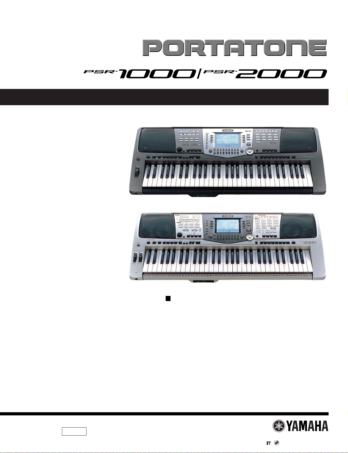
PSR-2000
SERVICE MANUAL
PK
001666
HAMAMATSU, JAPAN
1.421K-4071 Printed in Japan '01.09
CONTENTS
SPECIFICATIONS···································································· 2
PANEL LAYOUT······································································· 4
CIRCUIT BOARD LAYOUT······················································ 6
DISASSEMBLY PROCEDURE················································· 8
LSI PIN DESCRIPTION·························································· 13
IC BLOCK DIAGRAM ····························································· 20
CIRCUIT BOARDS································································· 21
TEST PROGRAM··································································· 39
SYSTEM RESET···································································· 42
MIDI IMPLEMENTATION CHART·········································· 43
MIDI DATA FORMAT······························································ 44
PARTS LIST
BLOCK DIAGRAM
OVERALL CIRCUIT DIAGRAM
This document is printed on chlorine free (ECF) paper with soy ink.
PSR-1000
Page 2
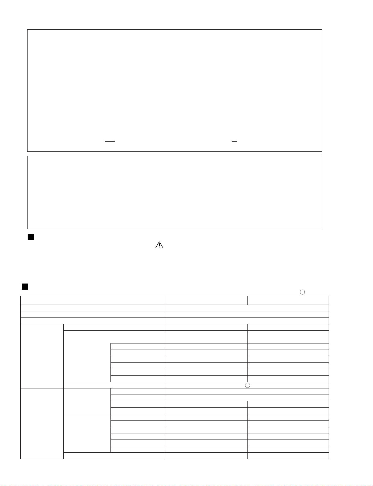
SPECIFICATIONS
PSR-1000/PSR-2000
2
WARNING: CHEMICAL CONTENT NOTICE!
The solder used in the production of this product contains LEAD. In addition, other electrical/electronic and/or plastic (where
applicable) components may also contain traces of chemicals found by the California Health and Welfare Agency (and possibly
other entities) to cause cancer and/or birth defects or other reproductive harm.
DO NOT PLACE SOLDER, ELECTRICAL/ELECTRONIC OR PLASTIC COMPONENTS IN YOUR MOUTH FOR ANY REASON
WHAT SO EVER!
Avoid prolonged, unprotected contact between solder and your skin! When soldering, do not inhale solder fumes or expose eyes
to solder/flux vapor!
If you come in contact with solder or components located inside the enclosure of this product, wash your hands before handling
food.
IMPORTANT NOTICE
This manual has been provided for the use of authorized Yamaha Retailers and their service personnel. It has been assumed that
basic service procedures inherent to the industry, and more specifically Yamaha Products, are already known and understood by
the users, and have therefore not been restated.
WARNING: Failure to follow appropriate service and safety procedures when servicing this product may result in personal
injury, destruction of expensive components and failure of the product to perform as specified. For these
reasons, we advise all Yamaha product owners that all service required should be performed by an authorized
Yamaha Retailer or the appointed service representative.
IMPORTANT: This presentation or sale of this manual to any individual or firm does not constitute authorization, certification,
recognition of any applicable technical capabilities, or establish a principal-agent relationship of any form.
The data provided is belived to be accurate and applicable to the unit(s) indicated on the cover. The research engineering, and
service departments of Yamaha are continually striving to improve Yamaha products. Modifications are, therefore, inevitable and
changes in specification are subject to change without notice or obligation to retrofit. Should any discrepancy appear to exist,
please contact the distributor's Service Division.
WARNING: Static discharges can destroy expensive components. Discharge any static electricity your body may have
accumulated by grounding yourself to the ground bus in the unit (heavy gauge black wires connect to this bus).
IMPORTANT: Turn the unit OFF during disassembly and parts replacement. Recheck all work before you apply power to the
unit.
WARNING
Components having special characteristics are marked and must be replaced with parts having specification equal to those
originally installed.
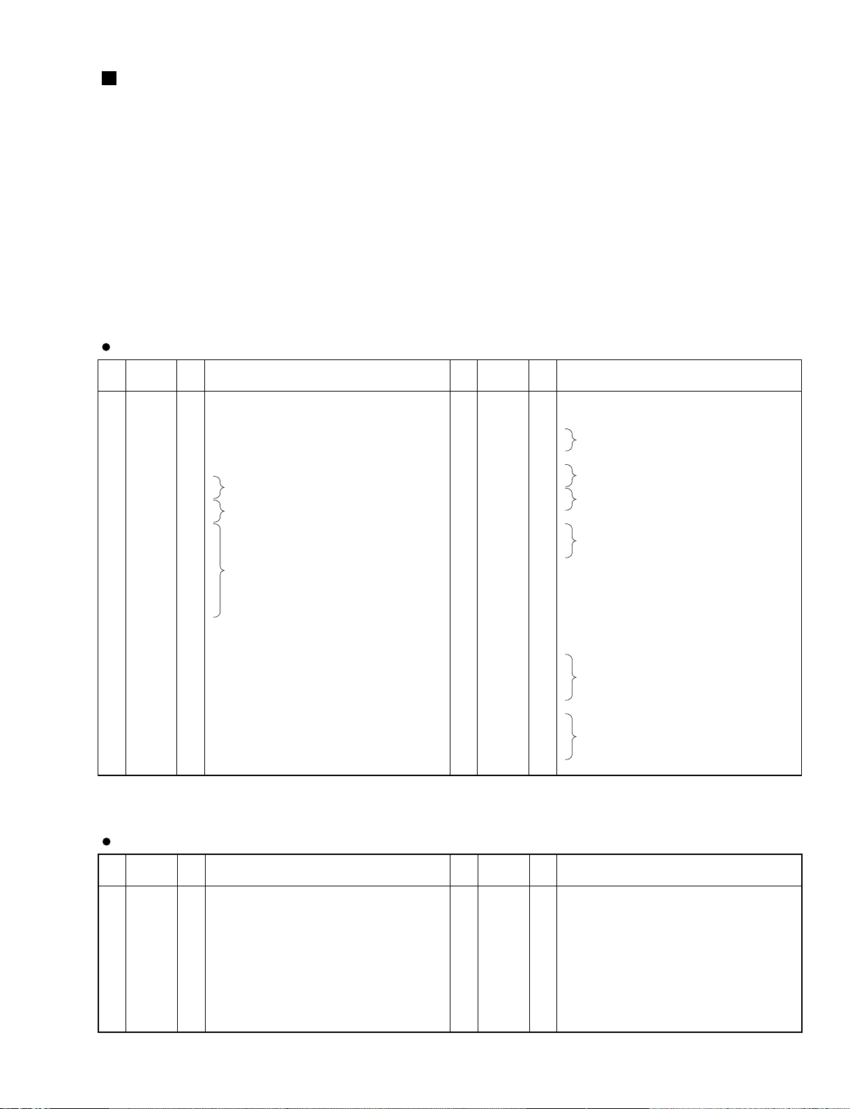
Model Name
Sound Source
Display
Keyboard
Voice Polyphony (max)
Voice Selection
Regular Voice
Sweet Voice
Cool Voice
Live Voice
Others
Organ Flute
Sound creator
Effects Reverb
Chorus
Effect Blocks
DSP
Microphone
REVERB
CHORUS
DSP1
Effect Types
DSP2, 3, 4
Master EQ
Part EQ
Vocal Harmony
PSR-1000 PSR-2000
AWM Dynamic Stereo Sampling
320 x 240 dots backlit graphic LCD
61 keys (C1 - C6 with Initial Touch)
32 64
233 voices + 480 XG voices 313 voices + 480 XG voices
+ 15 Drum Kits + 16 Drum Kits
233 303
38
12
—3
229 290
— 10 (8 Footages)
1
1
14
—1
23 Preset+3 User 29 Preset+3 User
15 Preset+3 User 25 Preset+3 User
98 Preset+3 User 164 Preset+3 User
— 88 Preset +10 User
— 5 Preset + 2 User
— 27 Parts
— 49 Preset +10 User
: available
Page 3
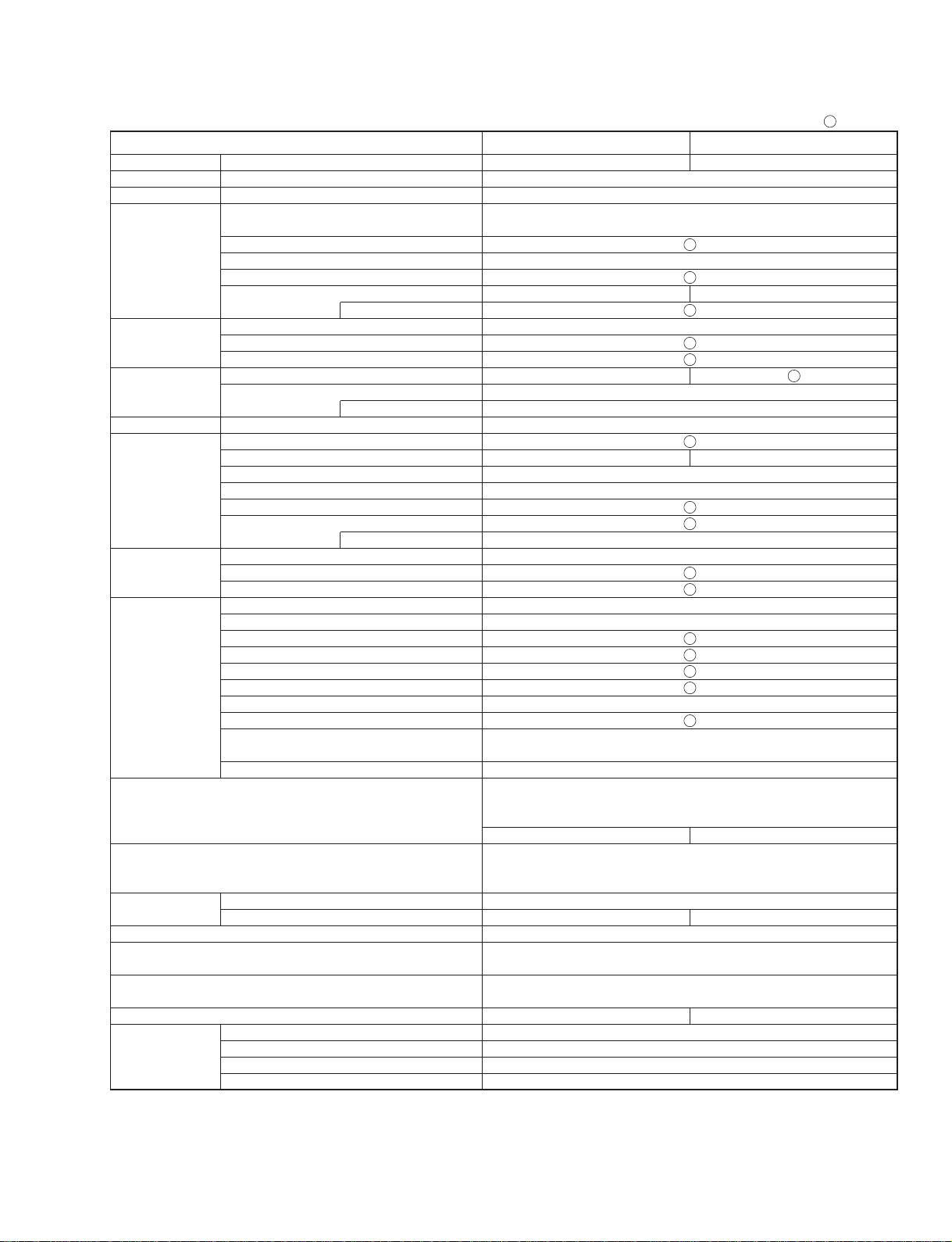
PSR-1000/PSR-2000
3
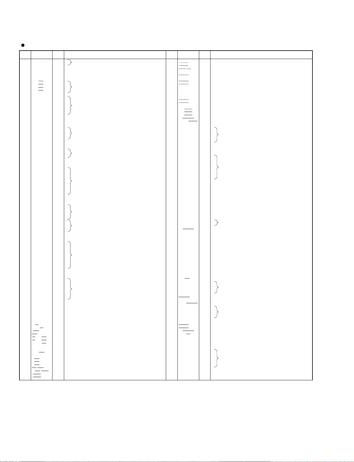
Model Name
Accompaniment Number of Accompaniment Styles
Style Number of Session Styles
Disk
Fingering
Style Creator
OTS (One Touch Setting)
OTS link
Music Finder
Edit
Song Format
Preset Songs
Lyrics
Score
Recording
Record Channels
Multi Pad Preset
Memory Floppy Disk (2HD,2DD)
Device Flash Memory (internal)
Flash Availability
Tempo Tempo Range
Tap Tempo
Metronome
Sound
Registration Buttons
Memory Regist Sequence
Freeze
Others Demo
Language
Help
Direct Access
Master Volume
Fade In/Out
Transpose
Tuning
Scale
Touch Response
Jacks/Connectors
Pedal Functions
Amplifiers/ Amplifiers
Speakers Speakers
Power Consumption
Power supply
Dimensions [W x D x H]
(without Music Stand)
Weight
Optional Headphones
accessories Foot Switch
Foot Controller
Keyboard Stand
PSR-1000 PSR-2000
169 181
4
28 styles (included in the accessory disk)
Single Finger, Fingered, Fingered On Bass, Multi Finger, AI Fingered,
Full Keyboard, AI Full Keyboard
4/Accompaniment Style
400 (max.) 500 (max.)
SMF (Format 0,1), ESEQ
—
Quick Recording, Multi Recording, Step Recording, Song Editing
16
4 Pads x 54 Banks
512KB 1MB
Song (SMF), Style (SFF), Registration, Voice, etc.
5 - 500
Bell on/off
8
Function, Voice, Style
6 languages (English, Japanese, German, French, Spanish, Italian)
Keyboard/Song/Master
Equal Temperament, Pure Major/Pure Minor, Pythagorean, Mean-Tone,
Werckmeister/Kirnberger, Arabic 1/2
5 level
DC IN, PHONES, MIDI (OUT, IN), TO HOST,
HOST SELECT SW, FOOT PEDAL1 (SWITCH), FOOT PEDAL2,
AUX OUT (LEVEL FIXED) (L/R), OUTPUT (L/L+R)
— MIC (INPUT VOLUME, MIC./ LINE)
VOLUME, SUSTAIN, SOSTENUTO, SOFT, GLIDE, PORTAMENTO,
PITCHBEND, MODULATION, DSP VARIATION, SONG START/STOP,
STYLE START/STOP, etc.
12 W x 2
(12 cm + 5 cm) x 2 [12 cm + 4 cm (dome)] x 2
31 W
Yamaha AC adaptor PA-300 (included)
*May not be in you area.Please check with your Yamaha dealer.
973 x 399 x 161 mm
[38-5/16" x 15-11/16" x 6-5/16"]
10.0 Kg (22 lbs., 1 oz) 10.5 Kg (23 lbs., 2 oz)
HPE-150
FC4 / FC5
FC7
L-6, L-7
: available
Page 4
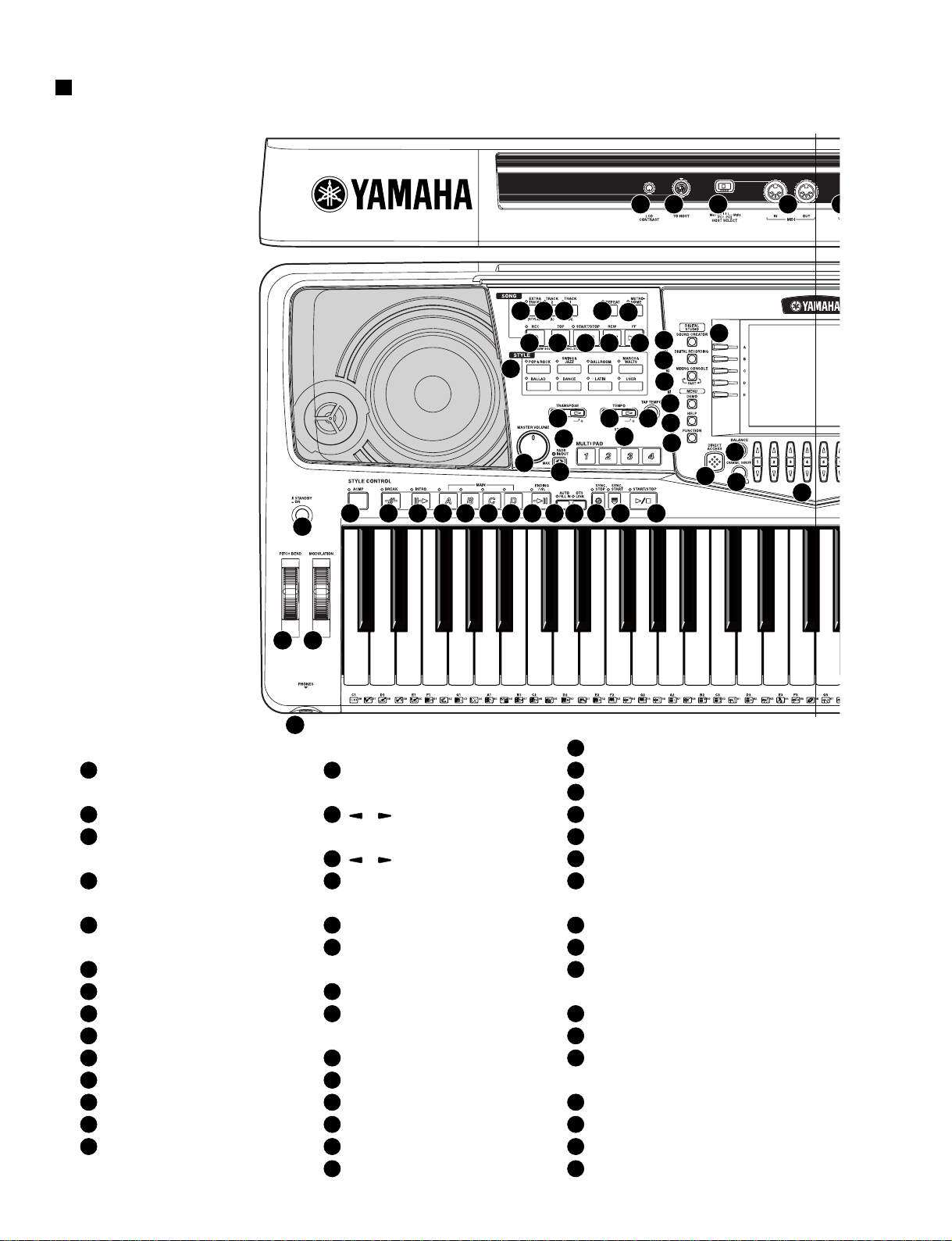
PSR-1000/PSR-2000
4
PANEL LAYOUT
A'
A
5
6 7 8 9
10
15
16
19
20
23 24 25 26 27 28 29 30 31 32 33 34 35
21
22
17 18
11 12 13 14
36
42
43
44
45
46
55 74 75 76 7
37
38
39
40
41
2 3
4
1
1
[STANDBY/ON] switch
POWER
15
STYLE buttons
STYLE
36
[SOUND CREATOR] button
37
[DIGITAL RECORDING] button
38
[MIXING CONSOLE] button
DIGITAL STUDIO
39
[DEMO] button
40
[HELP] button
41
[FUNCTION] button
MENU
42
[A] - [J] buttons
43
[DIRECT ACCESS] button
44
[BALANCE] button
45
[CHANNEL ON / OFF] button
DISPLAY CONTROL
29
MAIN [D] button
30
[ENDING / rit.] button
31
[AUTO FILL IN] button
32
[OTS LINK] button
33
[SYNC.STOP] button
34
[SYNC.START] button
35
[START / STOP] button
TRANSPOSE
17
[ ] [ ] buttons
18
[TAP TEMPO] button
TEMPO
19
[MASTER VOLUME] dial
20
[FADE IN / OUT] button
MASTER VOLUME
21
[1] - [4] buttons
22
[STOP] button
MULTI PAD
23
[ACMP] button
24
[BREAK] button
25
[INTRO] button
26
MAIN [A] button
27
MAIN [B] button
28
MAIN [C] button
STYLE CONTROL
2
PITCH BEND
3
MODULATION (PSR-2000 only)
WHEEL
4
[PHONES] jack
PHONES
5
[METRONOME] button
METRONOME
6
[EXTRA TRACKS (STYLE)] button
7
[TRACK 2 (L)] button
8
[TRACK 1 (R)] button
9
[REPEAT] button
10
[REC] button
11
[TOP] button
12
[START / STOP] button
13
[REW] button
14
[FF] button
SONG
16
[ ] [ ] buttons
Page 5
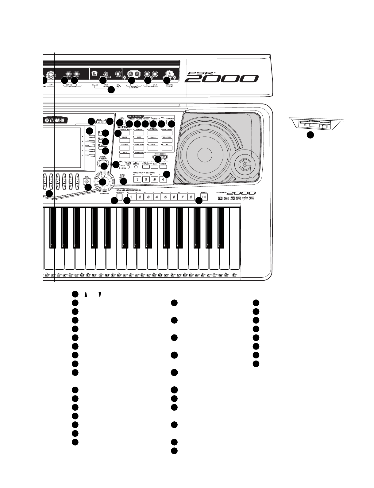
PSR-1000/PSR-2000
5
A'
A
46
42
47
73
48
56
57 58 59 60 61 62
63
64
65
66
67
68 69 70
71
49
50
51
52
53
54
63
VOICE buttons
VOICE
74
[TO HOST] terminal
75
[HOST SELECT] switch
76
MIDI [OUT] [IN] terminals
77
[FOOT PEDAL 1 (SWITCH) ] jack
78
[FOOT PEDAL 2] jack
79
AUX OUT (LEVEL FIXED) [L] [R] jacks
80
OUTPUT [L / L+R] [R] jacks
81
DC IN terminal
Connectors
64
[UPPER OCTAVE] button
UPPER OCTAVE
65
MIC. buttons (PSR-2000 only)
MIC.
66
[MUSIC FINDER] button
MUSIC FINDER
67
[1] - [4] buttons
ONE TOUCH SETTING
68
[FREEZE] button
69
[1] – [8] buttons
70
[MEMORY] button
REGISTRATION MEMORY
71
Floppy disk drive (3.5”)
FLOPPY DISK
72
[INPUT VOLUME] knob
73
[MIC. / LINE IN] jack
Microphone (PSR-2000 only)
56
[LEFT HOLD] button
57
[TOUCH] button
58
[SUSUTAIN] button
59
[HARMONY / ECHO] button
60
[MONO] button
61
[DSP] button
62
[VARIATION] button
VOICE EFFECT
46
[1 ] - [8 ] buttons
47
[BACK] button
48
[NEXT] button
49
VOICE PART ON / OFF [MAIN] button
50
VOICE PART ON / OFF [LAYER] button
51
VOICE PART ON / OFF [LEFT] button
52
[ENTER] button
53
[DATA ENTRY] dial
54
[EXIT] button
55
[LCD CONTRAST] knob
Page 6
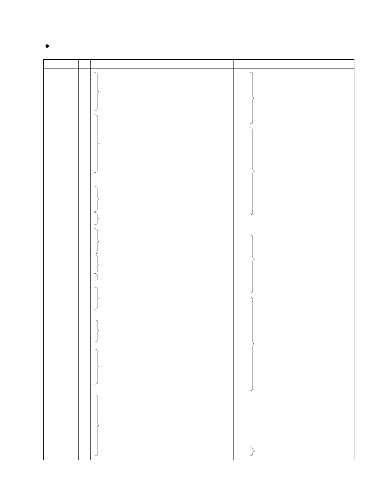
WH008
WH007
DM
VR
INV
AM
SW
HP
WH003
170
WH002
WH013
WH007
U410
LCD
Keyboard assembly
Speaker L (Tweeter)
PN1
PN2
ENC
PN3
PB1
PB2
MOD
PN4
MKS5F
MK-LMK-H
370
L110
180WH012U380U370
L160
L170
WH006WH005S5 150 160S6
S4
S7
160
U370 U380 WH013 U390U410
WH001
WH010
WH010
WH011
WH009
U400 WH005
<PSR-1000> <PSR-2000>
Speaker R (Tweeter)
Speaker R (Woofer)
Speaker L (Woofer)
Upper case assembly
Lower case assembly
PSR-1000/PSR-2000
6
CIRCUIT BOARD LAYOUT
Page 7
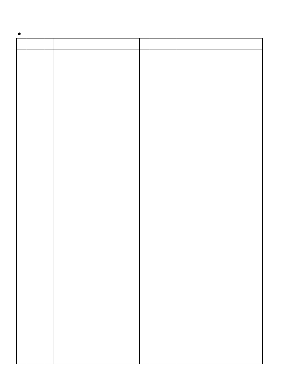
U410
WH005
L160
L170
U370
U380
WH001
WH002
WH003
WH006
WH009
WH010
WH011
WH012
WH013
Speaker (Woofer)
MKS5F-CN1 *1 *1
*1 *2
*1
*1 *1
*2
*1
*1
*1
*1
*1
*1
*1
*1
*1
*1
*2
Speaker (Tweeter)
AM-CN110
DM-CN102
AM-CN109
5P L=800
6P
4P L=800
SP
KB
TW
Connector AssemblyPart No.
(V778250)
(V778240)
(V778260)
Location Destination Remarks
LCD
VR-CN100
FDD
FDD
PN1-CN2
PN1-CN1
PN2-CN7
AM-CN303
AM-CN300
DM-CN500 14P
AM-CN102 5P L=480
DM-CN300 34P
DM-CN103 3P L=700
DM-CN600 26P
DM-CN100 21P
PN1-CN5 10P L=200
DM-CN501 3P L=120
DM-CN109 11P L=120
LCD
VOL
FD
FDPS
PN1
PN2
PN5
CNT
DJ
(V815820)
S4
MK-L MKS5F-CN2 12PCableVU958900
S5
MK-L MK-H 12PCableVU659500
S6
MK-L MKS5F-CN3 7PCableVU659400
S7
MK-H MKS5F-CN4 5PCableVU659600
(V778150)
V7782900
V7780900
(V778070)
(V778080)
(V778110)
(V778120)
(V778130)
AM-CN106 DM-CN105 5P L=120PS(V778160)
ENC-CN13 PN1-CN4 3P L=100ENC(V778190)
PB1-CN15
PN3-CN10
PB2-CN16
3P L=130
3P L=130
(PSR-1000)
(PSR-2000)
(PSR-2000)
(PSR-2000)
(PSR-2000)
PB(V778200)
MOD-CN14 PN3-CN11 4P L=130MOD(V778210)
AM-CN101 DM-CN700 4P L=300MIC(V778220)
PN1-CN6 AM-CN107 3P L=480IND(V778230)
* The parts with “( )” in “Part No.” are not available as service parts.
*1:
*2:
Edge mark is adjusted to Pin 1 mark ( mark).
Red wire is adjusted to Pin 1 mark ( mark).
L110
150
160
INV-CN1 DM-CN104 2P L=200INVP(V778270)
170
INV-CN2 LCD 4P L=100INV(V778280)
180
AM-CN103
PN1-CN3
PN3-CN9
DM-CN908
PN3-CN8
PN4-CN12
9P
28P 300mm
11P 100mm
AN2
CARD
CARD
(V815810)
MFA28300
MFA11100
370
U390
U400
WH007
HP-CN111 AM-CN108 5P L=380HP(V778170)
WH008
SW-CN104 AM-CN105 6P L=320SW(V778180)
PSR-1000/PSR-2000
7
Page 8
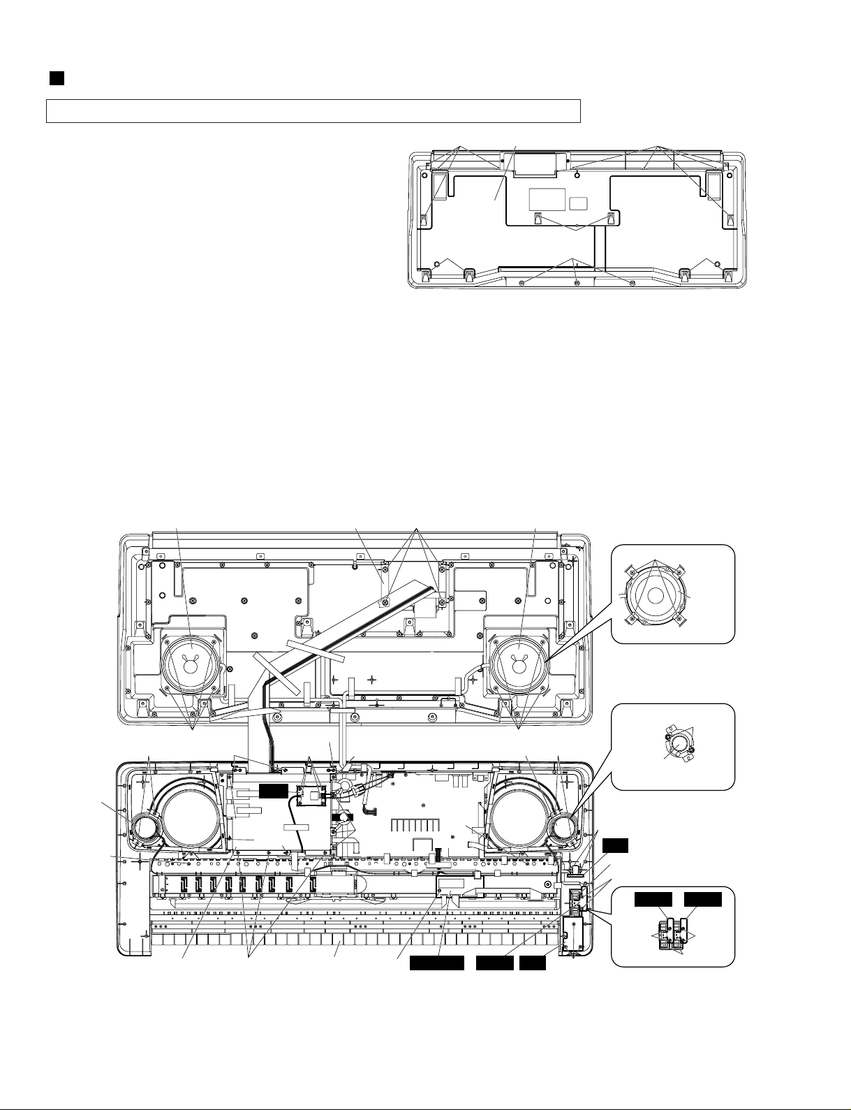
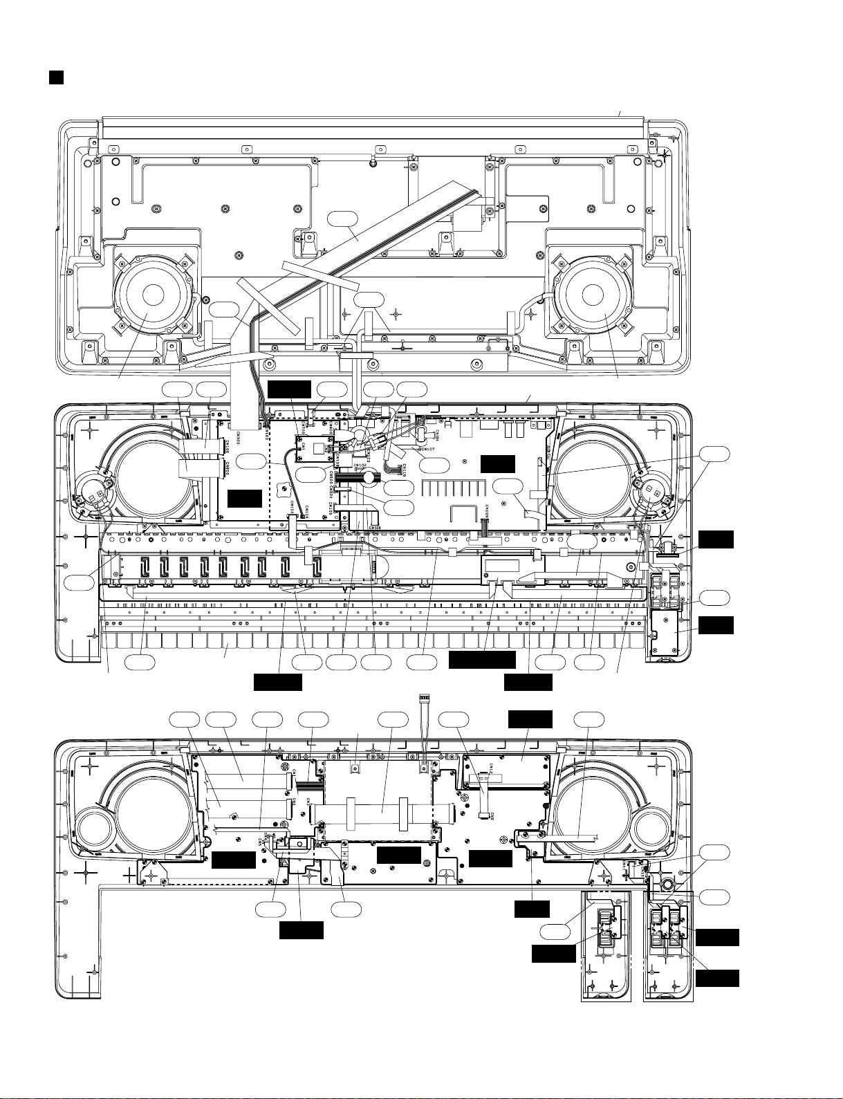
[270A]
[250B]
[30]
[510A]
[340]
[270B][260A][270C]
[270C]
[270C]
[100A]
[50] Woofer LFloppy disk drive assembly
Keyboard assembly
Wheel assembly
Shield cover L
[270B]
[100A]
Woofer R
[250B]
[260B]
[260B]
[260B]
[260B]
* This figure shows the PSR-1000.
[100B]
* PSR-2000
Woofer
[30]: Bind Head Tapping Screw-P 3.0x16 MFZN2BL (EP630220)
[50]: Bind Head Tapping Screw-P 4.0x16 MFZN2Y (VM839600)
[100]: Bind Head Tapping Screw-P 4.0x10 MFZN2Y (EP640500)
[250B]: Bind Head Tapping Screw-P 3.0x25 MFZN2Y (VK228100)
[260]: Bind Head Tapping Screw-B 3.0x6 MFZN2Y (EP600130)
[270]: Bind Head Tapping Screw-P 3.0x8 MFZN2Y (EP600280)
[290]: Bind Head Tapping Screw-B 4.0x6 MFZN2BL (EP600370)
[340]: Flat Head Tapping Screw-B 3.0x8 MFZN2Y (EP600420)
[510]: Bind Head Tapping Screw-P 3.0x8 MFZN2Y (EP600280)
Tweeter R
Tweeter L
INV
HPMKS5F
[290]
Tweeter
* PSR-2000
SW
PB2
[510B] [510A]
Wheel
* PSR-2000
PB1MOD
(Fig. 2)
PSR-1000/PSR-2000
8
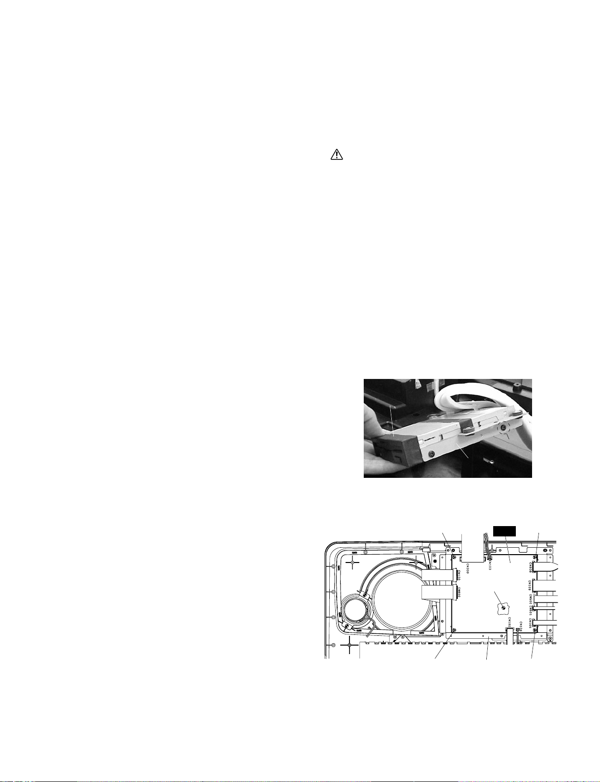
DISASSEMBLY PROCEDURE
1. Lower Case Assembly (Time required: About
5 minutes)
1-1 Remove the sixteen (16) screws marked [240] and the two
(2) screws marked [250A]. The lower case assembly can
then be removed. (Fig. 1)
2. HP Circuit Board
(Time required: About 10 minutes)
2-1 Remove the lower case assembly. (See procedure 1.)
2-2 Remove the three (3) screws marked [270A]. The HP
circuit board can then be removed. (Fig. 2)
3. Wheel Assembly, PB2 Circuit Board (PSR-
1000), PB1 Circuit Board (PSR-2000)
(Time required: About 10 minutes)
3-1 Remove the lower case assembly. (See procedure 1.)
3-2 Remove the two (2) screws marked [510A]. The PB2 ( or
PB1) circuit board with the wheel assembly can then be
removed. (Fig. 2)
3-3 Remove the wheel assembly from the PB2 (or PB1)
circuit board. (Fig. 3)
4. MOD Circuit Board (PSR-2000 only)
(Time required: About 10 minutes)
4-1 Remove the lower case assembly. (See procedure 1.)
4-2 Remove the two (2) screws marked [510B]. The MOD
circuit board with the wheel can then be removed. (Fig. 2)
4-3 Remove the wheel from the MOD circuit board. (Fig. 3)
(Fig. 1)
[240]: Bind Head Tapping Screw-P 3.0x12 MFZN2Y (EP600300)
[250A]: Bind Head Tapping Screw-P 3.0x25 MFZN2Y (VK228100)
[240]
[240] [240] [240]
[250A]
[240]Lower case assembly
Caution: Be sure to attach the removed filament tape just as it was before removal.
Page 9
5. SW Circuit Board
(Time required: About 10 minutes)
5-1 Remove the lower case assembly. (See procedure 1.)
5-2 Remove the two (2) screws marked [340]. The SW circuit
board can then be removed. (Fig. 2)
5-3 Remove the red knob from the SW circuit board.
6. Tweeter (PSR-1000)
(Time required: About 10 minutes)
6-1 Remove the lower case assembly. (See procedure 1.)
6-2 Remove the two (2) screws marked [270B]. The tweeter
can then be removed. (Fig. 2)
* The left and right tweeters can be removed in the respectively
same method.
7. Tweeter (PSR-2000)
(Time required: About 10 minutes)
7-1 Remove the lower case assembly. (See procedure 1.)
7-2 Remove the two (2) screws marked [290]. The tweeter can
then be removed. (Fig. 2)
* The left and right tweeters can be removed in the respectively
same method.
8. Woofer (PSR-1000)
(Time required: About 10 minutes)
8-1 Remove the lower case assembly. (See procedure 1.)
8-2 Remove the four (4) screws marked [100A]. The woofer
can then be removed. (Fig. 2)
* The left and right woofers can be removed in the respectively
same method.
9. Woofer (PSR-2000)
(Time required: About 10 minutes)
9-1 Remove the lower case assembly. (See procedure 1.)
9-2 Remove the four (4) screws marked [100B]. The woofer and
the four (4) speaker holders can then be removed. (Fig. 2)
* The left and right woofers can be removed in the respectively
same method.
10. Floppy Disk Drive
(Time required: About 10 minutes)
10-1 Remove the lower case assembly. (See procedure 1.)
10-2 Remove the four (4) screws marked [50]. The floppy disk
drive assembly can then be removed. (Fig. 2)
10-3 Remove the four (4) screws marked [F40]. The left and right
FDD holders can then be removed from the floppy disk
drive. (Fig. 3)
11. Keyboard Assembly
(Time required: About 10 minutes)
11-1 Remove the lower case assembly. (See procedure 1.)
11-2 Remove the two (2) screws marked [250B]. The keyboard
assembly can then be removed. (Fig. 2)
12. INV Circuit Board
(Time required: About 10 minutes)
ATTENTION: High Voltage
12-1 Remove the lower case assembly. (See procedure 1.)
12-2 Remove the four (4) screws marked [260A]. The INV
circuit board can then be removed. (Fig. 2)
13. DM Circuit Board, Shield Cover L and U
(Time required: About 15 minutes)
13-1 Remove the lower case assembly. (See procedure 1.)
13-2 Remove the INV circuit board. (See procedure 12.)
13-3 Remove the eight (8) screws marked [260B] and the five
(5) screws marked [270C]. The shield cover L can then be
removed. (Fig. 2)
13-4 Remove the four (4) screws marked [260C]. The DM
circuit board can then be removed. (Fig. 4)
13-5 Remove the screw marked [270D]. The shield cover U can
then be removed. (Fig. 4)
[F40]: Bind Head Tapping Screw 3.0x6 MFZN2BL (EG330360)
[F40]x4
(Fig. 3)
Floppy disk drive
FDD holder R
Shield cover U
[270D]
[260C]
[260C] [260C]
(Fig. 4)
[260C]: Bind Head Tapping Screw-B 3.0x6 MFZN2Y (EP600130)
[270D]: Bind Head Tapping Screw-P 3.0x8 MFZN2Y (EP600280)
DM
[260C]
PSR-1000/PSR-2000
9
Page 10
[510D]
[510D]
[510E]
[510C]
[510E]
[510E]
[510C] [510E] [510I] [510I]
[510G] [510G]
[510H]
[510I]
[270F]
[510I] [510J] [510J]
[510I]
[510F]
[510K]
Keyboard support (A) Keyboard support (B)
Panel angle bracket DM holder
[260D]: Bind Head Tapping Screw-B 3.0x6 MFZN2Y (EP600130)
[270E]: Bind Head Tapping Screw-P 3.0x8 MFZN2Y (EP600280)
[280]: Bind Head Tapping Screw-B 3.0x6 MFZN2BL (EP600230)
[260D]
[270E] [270E]
[260D]
[270E]
[280]
• Rear view
(Fig. 5)
[270F]: Bind Head Tapping Screw-P 3.0x8 MFZN2Y (EP600280)
[510]: Bind Head Tapping Screw-P 3.0x8 MFZN2Y (EP600280)
(Fig. 7)
(Fig. 6)
AM
PN1
PN2
PN4
PN3
Volume knob
VR
LCD
PSR-1000/PSR-2000
10
14. AM Circuit Board
(Time required: About 15 minutes)
14-1 Remove the lower case assembly. (See procedure 1.)
14-2 Remove the INV circuit board. (See procedure 12.)
14-3 Remove the shield cover L, the DM circuit board and the
shield cover U. (See procedure 13.)
14-4 Remove the two (2) screws marked [260D], the nine (9)
screws marked [270E] and the four (4) screws marked
[280]. The AM circuit board can then be removed. (Fig. 5)
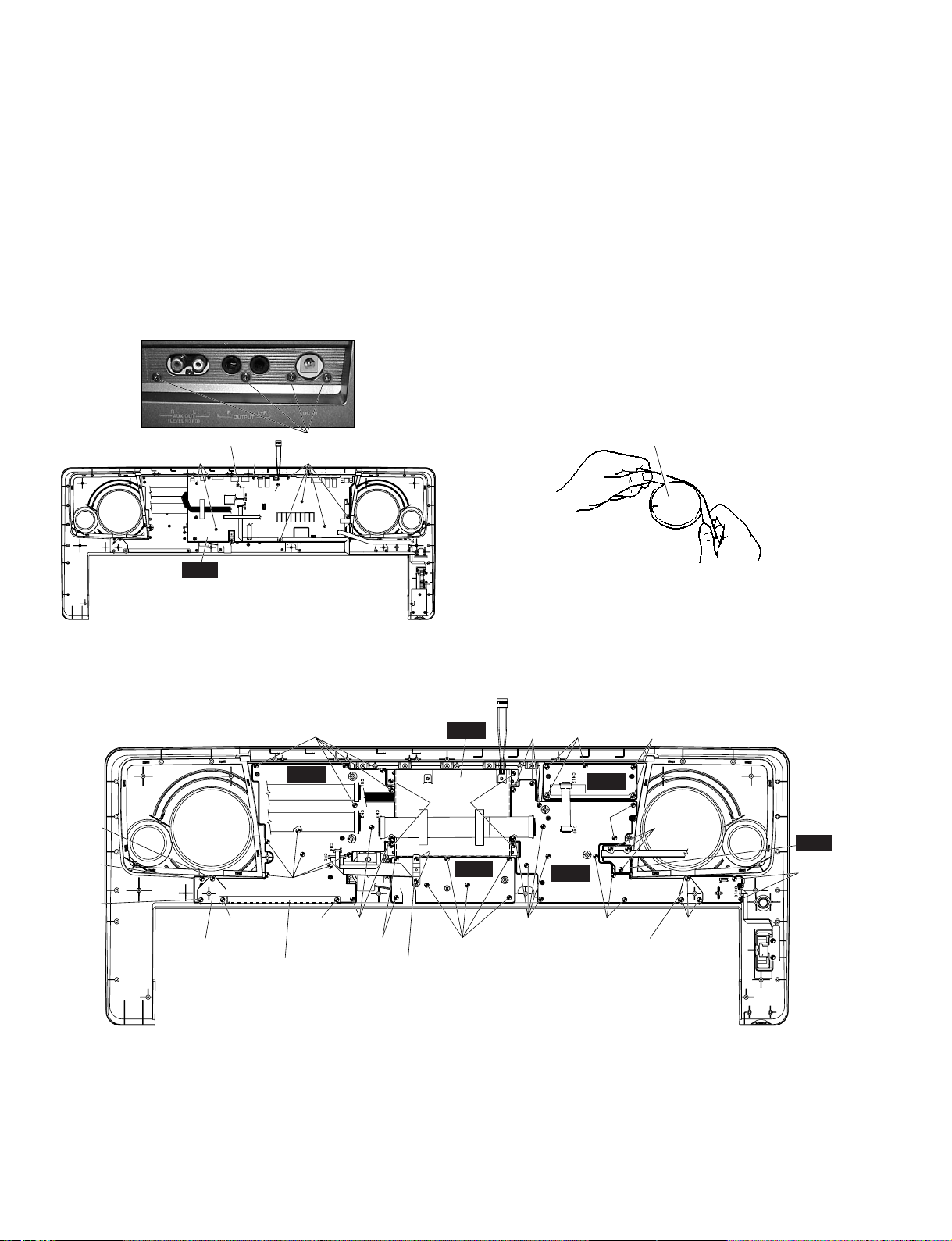
15. VR, ENC, PN1, PN2, PN3, PN4 Circuit Boards and LCD
15-1 Remove the lower case assembly. (See procedure 1.)
15-2 Remove the INV circuit board. (See procedure 12.)
15-3 Remove the shield cover L, the DM circuit board and the
shield cover U. (See procedure 13.)
15-4 Remove the AM circuit board. (See procedure 14.)
15-5 VR Circuit Board
(Time required: About 20 minutes) :
15-5-1 Remove the volume knob from the control panel side.
(Fig. 6)
15-5-2 Remove the three (3) screws marked [270F]. The VR
circuit board can then be removed. (Fig. 7)
Page 11
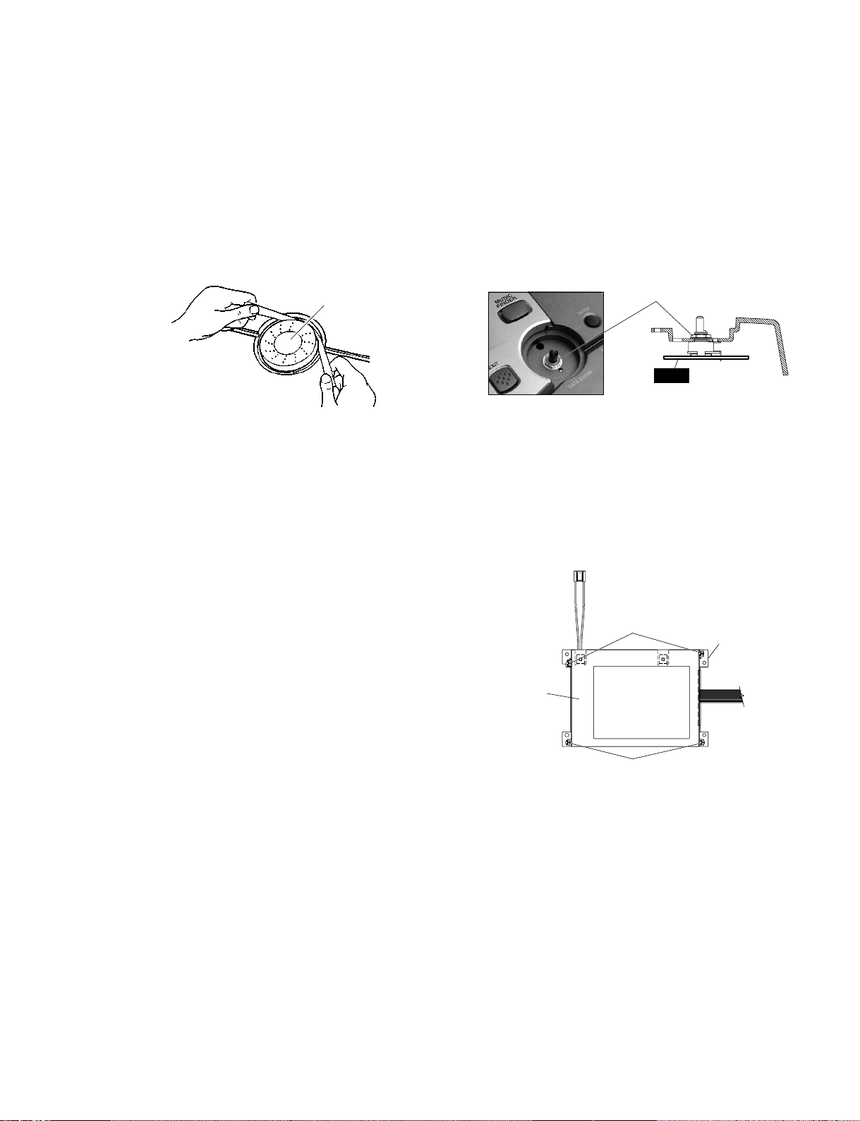
15-6 ENC Circuit Board
(Time required: About 20 minutes) :
15-6-1 Remove the encoder knob from the control panel side.
(Fig. 8)
15-6-2 Remove the hexagonal nut marked [A]. The ENC circuit
board can then be removed. (Fig. 9)
15-7 PN1 Circuit Board
(Time required: About 25 minutes) :
15-7-1 Remove the keyboard assembly. (See procedure 11.)
15-7-2 Remove the two (2) screws marked [510C]. The panel
angle blacket can then be removed. (Fig. 7)
15-7-3 Remove the two (2) screws marked [510D]. The keyboard
support (A) can then be removed. (Fig. 7)
15-7-4 Remove the fifteen (15) screws marked [510E]. The PN1
circuit board can then be removed. (Fig. 7)
PSR-1000/PSR-2000
11
15-8 PN2 Circuit Board
(Time required: About 25 minutes) :
15-8-1 Remove the keyboard assembly. (See procedure 11.)
15-8-2 Remove the two (2) screws marked [510F]. The DM
holder can then be removed. (Fig. 7)
15-8-3 Remove the seven (7) screws marked [510G]. The PN2
circuit board can then be removed. (Fig. 7)
15-9 PN3 Circuit board
(Time required: About 25 minutes) :
15-9-1 Remove the keyboard assembly. (See procedure 11.)
15-9-2 Remove the three (3) screws marked [510H]. The
keyboard support (B) can then be removed. (Fig. 7)
15-9-3 Remove the fifteen (15) screws marked [510I]. The PN3
circuit board can then be removed. (Fig. 7)
15-10 PN4 Circuit board
(Time required: About 20 minutes) :
15-10-1
Remove the five (5) screws marked [510J]. The PN4
circuit board can then be removed. (Fig. 7)
15-11 LCD (Time required: About 20 minutes) :
15-11-1
Remove the four (4) screws marked [510K]. The LCD can
then be removed with the LCD holder. (Fig. 7)
15-11-2
Remove the four (4) screws marked [500]. The LCD
holder can then be removed from the LCD. (Fig. 10)
ENC
[A]
(Fig. 8) (Fig. 9)
Encoder knob
[500]: Bind Head Tapping Screw-B 3.0x6 MFZN2Y (EP600130)
(Fig. 10)
LCD holder
LCD
[500]
[500]
Page 12
PSR-1000/PSR-2000
12
[140]: Bind Head Tapping Screw-P 3.0x16 MFZN2BL (VB205200)
[140]: Bind Head Tapping Screw-P 3.0x16 MFZN2B (VS756700)
(Fig. 12) (Fig. 15)
MK-L MK-H,
MK-L MK-H,
Hooks A
Hooks B
Black key
Black key
Rubber contact
Rubber contact
Rubber contact
White key
White key C'
White key CEGB
White key DFA
(Fig. 11) (Fig. 13)
(Fig. 14)
[140]
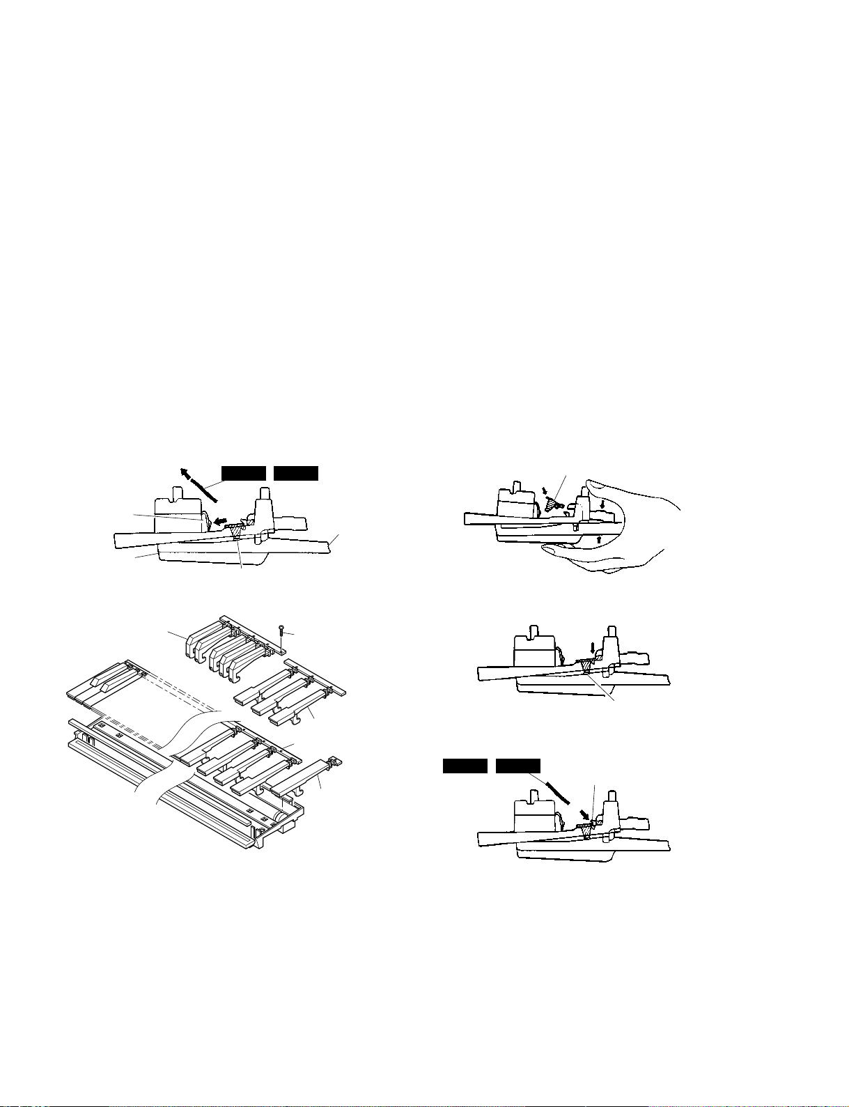
16. Disassembling the Keyboard Assembly
16-1 Remove the Keyboard assembly. (See procedure 11.)
16-2 Remove the two (2) screws marked [30]. The MKS5F
circuit board can then be removed. (Fig. 2)
* Be sure to make a correct match when connecting
MKS5F (CN1) and DM (CN102).
Connecting the connectors in the wrong way
around may cause damage to the MKS5F circuit
board.
16-3 Remove the MK-L and MK-H circuit board while
pressing the fifteen (15)hooks A inward, and then remove
the rubber contact. (Fig. 11)
16-4 Remove the twenty-one (21) screws marked [140], then
removw the black keys from the lower notes. Afterwards,
remove the white keys DFA and C' and then remove the
white keys CEGB from the higer notes. At this time, lift
the keys from the front and slide them towards you. The
keys can then be removed from the assembly. (Fig. 12)
17. Assembling the Keyboard Assembly
17-1 Install the white keys CEGB from the lower notes, and
then install the DFA keys and C' key. Afterwards install
the black keys from the higher notes, and tighten the
twenty-one (21) screws marked [140]. (Fig. 12)
17-2 Install the rubber contacts in the assembly while pressing
the keys as shown in Figure13. Check that the rubber
contact has been firmly placed into position in the area
indicated by the arrow in Figure 14. When fitting the
rubber contacts, raise both ends of the frame so that keys
do not push the rubber contact up.
17-3 Install the MK-L and MK-H circuit boards in the assembly
so that the hooks B hold it as shown in Figure 15.
Page 13
PIN
NO.
I/O FUNCTIONNAME
PIN
NO.
I/O FUNCTIONNAME
1
2
3
4
5
6
7
8
9
10
11
12
AINR+
AINRVREF
VA
AGND
AINL+
AINLTST1
HPFE
TST2
TST3
VD
I
I
O
-
I
I
I/O
I/O
I/O
-
Analog signal input (R channel +)
Analog signal input (R channel -)
Reference voltage
Analog power supply
Analog ground
Analog signal input (L channel +)
Analog signal input (L channel -)
Test mode setting 1
HPF on/off
Test mode setting 2
Test mode setting 3
Digital power supply
13
14
15
16
17
18
19
20
21
22
23
24
DGND
TST4
AMODE2
/PD
MCLK
SCLK
LRCK
FSYNC
SDATA
CMODE
SMODE1
VB
-
I/O
I
I
I/O
I
I/O
O
I
I
-
Digital ground
Test mode setting 4
Interface clock select 2
Power-down mode
Master clock input
Serial data clock
Input/Output channel clock
Frame synch. clock
Serial data output
Master clock select
Interface clock select 1
Digital power supply
AK5351-VF-E2 (XV510A00) ADC (Analog to Digital Converter)
DM: IC800 (PSR-2000)
PIN
NO.
I/O FUNCTIONNAME
PIN
NO.
I/O FUNCTIONNAME
1
2
3
4
5
6
7
8
9
10
11
12
13
14
15
16
17
18
19
20
21
22
23
24
25
26
27
28
29
30
31
32
8"//5"
XTALSET
/RESET
E//RD
RW//WR
/CS
/DACK
RS0
RS1
VSS1
VSS2
D0
D1
D2
D3
D4
D5
D6
D7
/DREQ
/IRQ
/DEND
VSS3
1/2 EX1
VCC1
NUM1
NUM3
IFS
SFORM
/INP
/READY
/WPRT
I
I
I
I
I
I
I
I
I
I/O
I/O
I/O
I/O
I/O
I/O
I/O
I/O
O
O
I
I
I
I
I
I
I
I
Data transmission speed
Clock select
Rest
Enable/Read
Read/write/Write
Chip select
DMA acknowledge
Register select
Ground
Data bus
DMA request
Interrupt request
Data end
Ground
Power supply
Host interface select
Format data
Index pulse
Ready from FDD
Write control signal
33
34
35
36
37
38
39
40
41
42
43
44
45
46
47
48
49
50
51
52
53
54
55
56
57
58
59
60
61
62
63
64
/TRKO
/INDEX
/RDATA
XTAL2
EXTAL2
NC
XTAL1
EXTAL1
VSS4
VSS5
NC
VCC2
VCC3
VCC4
/WGATE
/WDATA
VSS6
/STEP
/HDIR
/HLOAD
/HSEL
VSS7
/DS0
/DS1
/DS2
/DS3
VSS8
/MON0
/MON1
/MON2
/MON3
VSS9
I
I
I
O
O
O
O
O
O
O
O
O
O
O
O
O
O
Track 00 signal
Index signal
Read data input from FDD
Clock
Clock
Ground
Power supply
Write control
Writ data to FDD
Ground
Step signal to control head of FDD
Direction
Head load
Head select
Ground
Drive select
Ground
Motor on
Ground
HD63266F (XI939A00) FDC (Floppy Disk Controller)
DM: IC300
LSI PIN DESCRIPTION
PSR-1000/PSR-2000
13
HD63266F (XI939A00) FDC················································································································· 13
AK5351-VF-E2 (XV510A00) ADC ········································································································ 13
HD6417709F80B (XV250B00) CPU····································································································· 14
TC203C760HF-002 (XS725A00) SWP30B·························································································· 15
HG73C205AFD (XU947C00) SWX00B································································································ 16
YSS236-F (XT013A00) VOP3·············································································································· 17
µPD789022GB-A15-8E (XZ560100) CPU KBS···················································································· 18
S1D13305F00B100 (XQ595A00) LCDC ······························································································ 18
AD1854JRSRL (XY782A00) DAC········································································································ 19
Page 14
PSR-1000/PSR-2000
14
PIN
NO.
I/O
FUNCTION
NAME
PIN
NO.
I/O
FUNCTION
NAME
1
2
3
4
5
6
7
8
9
10
11
12
13
14
15
16
17
18
19
20
21
22
23
24
25
26
27
28
29
30
31
32
33
34
35
36
37
38
39
40
41
42
43
44
45
46
47
48
49
50
51
52
53
54
55
56
57
58
59
60
61
62
63
64
65
66
67
68
69
70
71
72
73
74
75
76
77
78
79
80
81
82
83
84
85
86
87
88
89
90
91
92
93
94
95
96
97
98
99
100
101
102
103
104
MD1
MD2
Vcc (RTC)
XTAL2
EXTAL2
Vss (RTC)
NMI
IRQ0/IRL0/PTH[0]
IRQ1/IRL1/PTH[1]
IRQ2/IRL2/PTH[2]
IRQ3/IRL3/PTH[3]
IRQ4/PTH[4]
D31/PTB[7]
D30/PTB[6]
D29/PTB[5]
D28/PTB[4]
D27/PTB[3]
D26/PTB[2]
Vss
D25/PTB[1]
Vcc
D24/PTB[0]
D23/PTA[7]
D22/PTA[6]
D21/PTA[5]
D20/PTA[4]
Vss
D19/PTA[3]
Vcc
D18/PTA[2]
D17/PTA[1]
D16/PTA[0]
Vss
D15
Vcc
D14
D13
D12
D11
D10
D9
D8
D7
D6
Vss
D5
Vcc
D4
D3
D2
D1
D0
A0
A1
A2
A3
Vss
A4
Vcc
A5
A6
A7
A8
A9
A10
A11
A12
A13
Vss
A14
Vcc
A15
A16
A17
A18
A19
A20
A21
Vss
A22
Vcc
A23
Vss
A24
Vcc
A25
BS/PTK[4]
RD
WE0/DQMLL
WE1/DQMLU/WE
WE2/DQMUL/ICIORD/PTK[6]
WE3/DQMUU/ICIOWR/PTK[7]
RD/WR
PTE[7]
Vss
CS0
Vcc
CS2/PTK[0]
CS3/PTK[1]
CS4/PTK[2]
CS5/CE1A/PTK[3]
CS6/CE1B
CE2A/PTE[4]
CE2B/PTE[5]
I
I
I
O
I
I
I
I
I
I
I/O
I/O
I/O
I/O
I/O
I/O
-
I/O
I/O
I/O
I/O
I/O
I/O
I/O
I/O
I/O
I/O
I/O
I/O
I/O
I/O
I/O
I/O
I/O
I/O
I/O
I/O
I/O
I/O
I/O
I/O
I/O
I/O
O
O
O
O
-
O
-
O
O
O
O
O
O
O
O
O
-
O
-
O
O
O
O
O
O
O
-
O
-
O
-
O
-
O
I/O
O
O
O
I/O
I/O
O
I/O
-
O
I/O
I/O
I/O
I/O
O
I/O
I/O
System clock
Power supply (3.3 V)
Clock
Clock
Ground (0 V)
Interrupt request
Interrupt request
Interrupt request
Data bus/ I/O port B
Ground (0 V)
Interrupt request
Power supply (3.3 V)
Data bus/ I/O port B
Data bus/ I/O port A
Ground (0 V)
Data bus/ I/O port A
Power supply (3.3 V)
Data bus/ I/O port A
Ground (0 V)
Data bus
Power supply (3.3 V)
Data bus
Ground (0 V)
Data bus
Power supply (3.3 V)
Data bus
Address bus
Ground (0 V)
Address bus
Power supply (3.3 V)
Address bus
Ground (0 V)
Address bus
Power supply (3.3 V)
Address bus
Ground (0 V)
Address bus
Power supply (3.3 V)
Address bus
Ground (0 V)
Address bus
Power supply (3.3 V)
Address bus
Bus control/ I/O port K
Read strobe
Select signal/DQM (SDRAM)
Select signal/DQM (SDRAM)/PCMCIA WE
Select signal/DQM (SDRAM)/PCMCIA I/O read/ I/O port K
Select signal/DQM (SDRAM)/PCMCIA I/O write/ I/O port K
Read/Write signal
I/O port E
Ground (0 V)
Chip select
Power supply (3.3 V)
Chip select/ I/O port K
Chip select/ I/O port K
Chip select/ I/O port K
Chip select/CE1/ I/O port K
Chip select/CE1
Chip enable/ I/O port E
Chip enable/ I/O port E
105
106
107
108
109
110
111
112
113
114
115
116
117
118
119
120
121
122
123
124
125
126
127
128
129
130
131
132
133
134
135
136
137
138
139
140
141
142
143
144
145
146
147
148
149
150
151
152
153
154
155
156
157
158
159
160
161
162
163
164
165
166
167
168
169
170
171
172
173
174
175
176
177
178
179
180
181
182
183
184
185
186
187
188
189
190
191
192
193
194
195
196
197
198
199
200
201
202
203
204
205
206
207
208
CKE/PTK[5]
RAS3L/PTJ[0]
RAS2L/PTJ[1]
CASLL/CAS/PTJ[2]
Vss
CASLH/PTJ[3]
Vcc
CASHL/PTJ[4]
CASHH/PTJ[5]
DACK0/PTD[5]
DACK1/PTD[7]
CAS2L/PTE[6]
CAS2H/PTE[3]
RAS3U/PTE[2]
RAS2U/PTE[1]
PTE[0]
BACK
BREQ
WAIT
RESETM
PTH[5]/ADTRG
IOIS16/PTG[7]
PTG[6]
PTG[5]
PTG[4]
PTG[3]
PTG[2]
Vss
PTG[1]
Vcc
PTG[0]
PTF[7]/PINT[15]
PTF[6]/PINT[14]
PTF[5]/PINT[13]
PTF[4]/PINT[12]
PTF[3]/PINT[11]
PTF[2]/PINT[10]
PTF[1]/PINT[9]
PTF[0]/PINT[8]
MD0
Vcc (PLL1)
CAP1
Vss (PLL1)
Vss (PLL2)
CAP2
Vcc (PLL2)
PTH[6]
Vss
Vss
Vcc
XTAL
EXTAL
STATUS[0]/PTJ[6]
STATUS[1]/PTJ[7]
TCLK/PTH[7]
IRQOUT
Vss
CKIO
Vcc
TxD0/SCPT[0]
SCK0/SCPT[1]
TxD1/SCPT[2]
SCK1/SCPT[3]
TxD2/SCPT[4]
SCK2/SCPT[5]
RTS2/SCPT[6]
RxD0/SCPT[0]
RxD1/SCPT[2]
Vss
RxD2/SCPT[4]
Vcc
CTS2/IRQ5/SCPT[7]
PTC[7]/PINT[7]
PTC[6]/PINT[6]
PTC[5]/PINT[5]
PTC[4]/PINT[4]
Vss
WAKEUP/PTD[3]
Vcc
PTD[2]/RESETOUT
PTC[3]/PINT[3]
PTC[2]/PINT[2]
PTC[1]/PINT[1]
PTC[0]/PINT[0]
DRAK0/PTD[1]
DRAK1/PTD[0]
DREQ0/PTD[4]
DREQ1/PTD[6]
RESETP
CA
MD3
MD4
MD5
AVss
AN[0]/PTL[0]
AN[1]/PTL[1]
AN[2]/PTL[2]
AN[3]/PTL[3]
AN[4]/PTL[4]
AN[5]/PTL[5]
AVcc
AN[6]/DA[1]/PTL[6]
AN[7]/DA[0]/PTL[7]
AVss
I/O
I/O
I/O
I/O
-
I/O
I/O
I/O
I/O
I/O
I/O
I/O
I/O
I/O
I/O
O
I
I
I
I
I
I
I
I
I
I
-
I
-
I
I
I
I
I
I
I
I
I
I
-
-
-
-
-
-
I
-
-
-
O
I
I/O
I/O
I/O
O
-
I/O
-
O
I/O
O
I/O
I/O
I
I
-
I
I/O
I/O
I/O
I/O
-
I/O
I/O
I/O
I/O
I/O
I/O
I/O
I/O
I
I
I
I
I
I
I
-
I
I
I
I
I
I
I/O
I/O
-
CK enable (SDRAM)/ I/O port K
RAS/ I/O port J
RAS/ I/O port J
CAS (DRAM)/CAS (SDRAM)/ I/O port J
Ground (0 V)
CAS (DRAM)/ I/O port J
Power supply (3.3 V)
CAS (DRAM)/ I/O port J
CAS (DRAM)/ I/O port J
DMAC/ I/O port D
DMAC/ I/O port D
CAS (DRAM)/ I/O port E
CAS (DRAM)/ I/O port E
RAS/ I/O port E
RAS/ I/O port E
I/O port E
System clock
System clock
Bus control
Reset
I/O port H/Analog
Right protect/Input port G
I/O port G
Ground (0 V)
I/O port G
Power supply (3.3 V)
I/O port G
I/O port F/Port Interrupt request
System clock
Power supply (3.3 V)
Clock
Ground (0 V)
Ground (0 V)
Clock
Power supply (3.3 V)
I/O port H
Ground (0 V)
Ground (0 V)
Power supply (3.3 V)
Clock
Clock
System clock
Timer
Interrupt request
Ground (0 V)
Clock
Power supply (3.3 V)
Forward data/Output port for SCI
Serial clock/ I/O port for SCI
Forward data/Output port for SCI
Serial clock/ I/O port for SCI
Transmit request/ I/O port for SCI
Reception data/Input port for SCI
Ground (0 V)
Reception data/Input port for SCI
Power supply (3.3 V)
Transmit clear/Interrupt request/Input port for SCI
I/O port C/Interrupt request
Ground (0 V)
Interrupt request/ I/O port D
Power supply (3.3 V)
I/O port D/Reset
I/O port C/Interrupt request
DMA request/ I/O port D
DMA request/ I/O port D
DMA request/ I/O port D
DMA request/ I/O port D
System clock
System clock
System clock
System clock
System clock
Analog ground (0 V)
A/D change input/Input port L
Analog power supply (3.3 V)
A/D change input/D/A change output/Input port L
Analog ground (0 V)
HD6417709F80B (XV250B00) CPU
DM: IC100
Page 15
PSR-1000/PSR-2000
15
PIN
NO.
I/O
FUNCTION
NAME
PIN
NO.
I/O
FUNCTION
NAME
1
2
3
4
5
6
7
8
9
10
11
12
13
14
15
16
17
18
19
20
21
22
23
24
25
26
27
28
29
30
31
32
33
34
35
36
37
38
39
40
41
42
43
44
45
46
47
48
49
50
51
52
53
54
55
56
57
58
59
60
61
62
63
64
65
66
67
68
69
70
71
72
73
74
75
76
77
78
79
80
81
82
83
84
85
86
87
88
89
90
91
92
93
94
95
96
97
98
99
100
101
102
103
104
105
106
107
108
109
110
111
112
113
114
115
116
117
118
119
120
Vss
CA0
CA1
CA2
CA3
CA4
CA5
CA6
CA7
CA8
CA9
CA10
CA11
VSS
CD0
CD1
CD2
CD3
CD4
CD5
CD6
CD7
CD8
CD9
CD10
CD11
CD12
CD13
CD14
VDD
VSS
CD15
CSN
WRN
RDN
VDD
SYSH0
SYSH1
SYSH2
SYSH3
SYSH4
SYSH5
SYSH6
SYSH7
KONO0
KONO1
KONO2
KONO3
VSS
SYSL0
SYSL1
SYSL2
SYSL3
SYSL4
SYSL5
SYSL6
SYSL7
KONI0
KONI1
VDD
VSS
KONI2
KONI3
DAC0
DAC1
WCLK
MELO0
MELO1
MELO2
MELO3
MELO4
MELO5
MELO6
MELO7
VDD
ADLR
MELI0
MELI1
MELI2
MELI3
MELI4
MELI5
MELI6
MELI7
VSS
RCASN
RA8
RA7
RA6
VDD
VSS
RA5
RA4
RA3
RA2
RA1
RA0
RRASN
RWEN
VSS
RD7
RD6
RD5
RD4
RD3
RD2
RD1
RD0
VSS
RD17
RD16
RD15
RD14
RD13
RD12
RD11
RD10
RD9
RD8
VDD
I
I
I
I
I
I
I
I
I
I
I
I
I/O
I/O
I/O
I/O
I/O
I/O
I/O
I/O
I/O
I/O
I/O
I/O
I/O
I/O
I/O
I/O
I
I
I
O
O
O
O
O
O
O
O
O
O
O
O
I/O
I/O
I/O
I/O
I/O
I/O
I/O
I/O
I
I
I
I
I
O
O
O
O
O
O
O
O
O
O
O
O
I
I
I
I
I
I
I
I
O
O
O
O
O
O
O
O
O
O
O
O
I/O
I/O
I/O
I/O
I/O
I/O
I/O
I/O
I/O
I/O
I/O
I/O
I/O
I/O
I/O
I/O
I/O
I/O
(Ground)
Address bus of internal register
(Ground)
Data bus of internal register
(Power supply)
(Ground)
Chip select
Write strobe
Read strobe
(Power supply)
NSYS/LNSYS upper 16 bits
Key on data
(Ground)
NSYS input/LNSYS output lower 8 bits
(Power supply)
Key on data input
(Ground)
DAC output
DAC0/DAC1 word clock
MEL wave data output
(Power supply)
ADC word clock
MEL wave data input
(Ground)
DRAM column address strobe
(Power supply)
(Ground)
DRAM address bus
DRAM row address strobe
DARM write enable
(Ground)
(Ground)
DRAM data bus
(Power supply)
121
122
123
124
125
126
127
128
129
130
131
132
133
134
135
136
137
138
139
140
141
142
143
144
145
146
147
148
149
150
151
152
153
154
155
156
157
158
159
160
161
162
163
164
165
166
167
168
169
170
171
172
173
174
175
176
177
178
179
180
181
182
183
184
185
186
187
188
189
190
191
192
193
194
195
196
197
198
199
200
201
202
203
204
205
206
207
208
209
210
211
212
213
214
215
216
217
218
219
220
221
222
223
224
225
226
227
228
229
230
231
232
233
234
235
236
237
238
239
240
VSS
HMD0
HMD1
HMD2
HMD3
HMD4
HMD5
HMD6
HMD7
HMD8
HMD9
HMD10
HMD11
HMD12
HMD13
HMD14
HMD15
VSS
HMA0
HMA1
HMA2
HMA3
HMA4
HMA5
HMA6
HMA7
HMA8
HMA9
HMA10
VSS
VDD
HMA11
HMA12
HMA13
HMA14
HMA15
HMA16
HMA17
HMA18
HMA19
HMA20
HMA21
HMA22
HMA23
HMA24
VSS
MRASN
MCASN
MOEN
MWEN
VSS
LMD0
LMD1
LMD2
LMD3
LMD4
LMD5
LMD6
LMD7
VDD
VSS
LMD8
LMD9
LMD10
LMD11
LMD12
LMD13
LMD14
LMD15
VSS
LMA0
LMA1
LMA2
LMA3
LMA4
LMA5
LMA6
LMA7
LMA8
LMA9
LMA10
LMA11
VSS
LMA12
LMA13
LMA14
LMA15
LMA16
LMA17
VDD
VSS
LMA18
LMA19
LMA20
LMA21
LMA22
LMA23
LMA24
VSS
SYO
SYOD
QCLK
HCLK
CK256
SYSCLK
VDD
SYI
MCLKI
MCLKO
VDD
XIN
XOUT
VSS
ICN
CHIP2
SLAVE
TESTON
ACIN
DCTEST
VDD
I/O
I/O
I/O
I/O
I/O
I/O
I/O
I/O
I/O
I/O
I/O
I/O
I/O
I/O
I/O
I/O
O
O
O
O
O
O
O
O
O
O
O
O
O
O
O
O
O
O
O
O
O
O
O
O
O
O
O
O
O
I/O
I/O
I/O
I/O
I/O
I/O
I/O
I/O
I/O
I/O
I/O
I/O
I/O
I/O
I/O
I/O
O
O
O
O
O
O
O
O
O
O
O
O
O
O
O
O
O
O
O
O
O
O
O
O
O
O
O
O
O
O
O
I
I
O
I
O
I
I
I
I
I
I
(Ground)
Wave memory data bus (Upper data memory)
(Ground)
(Ground)
(Power supply)
Wave memory address bus (Upper 16 bits)
(Ground)
RAS when DRAM(s) is connected to wave memory
CAS when DRAM(s) is connected to wave memory
Wave memory output enable
Wave memory write enable
(Ground)
Wave memory data bus (Lower data memory)
(Power supply)
(Ground)
(Ground)
(Ground)
Wave memory address bus (Lower data memory)
(Power supply)
(Ground)
(Ground)
Sync. signal for master clock
Sync. signal for HCLK/QCLK
1/12 master clock (64 Fs)
1/6 master clock (128 Fs)
1/3 master clock (256 Fs)
1/2 master clock (384 Fs)
(Power supply)
Sync. clock
Master clock input
Master clock output
(Power supply)
Crystal osc. input
Crystal osc. output
(Ground)
Initial clear
2 chips mode enable
Master/Slave select when 2 chips mode
Test pin
(Power supply)
TC203C760HF-002 (XS725A00) SWP30B (AWM Tone Generator coped with MEG)
Standard Wave Processor
DM: IC400 (PSR-2000 only)
Page 16
PIN
NO.
I/O FUNCTIONNAME
PIN
NO.
I/O FUNCTIONNAME
1
2
3
4
5
6
7
8
9
10
11
12
13
14
15
16
17
18
19
20
21
22
23
24
25
26
27
28
29
30
31
32
33
34
35
36
37
38
39
40
41
42
43
44
45
46
47
48
49
50
51
52
53
54
55
56
57
58
59
60
61
62
63
64
65
66
67
68
69
70
71
72
73
74
75
76
77
78
79
80
81
82
83
84
ICN
RFCLKI
TM2
AVDD_PLL
AVSS_PLL
MODE0
VCC7
GND8
XIN
XOUT
MODE1
TEST0
TESTON
AN0-P40
AN1-P41
AN2-P42
AN3-P43
AVDD_AN
AVSS_AN
TXD0
TXD1
EXCLK
SMD11
SMD4
SMD3
SMD12
SMD10
SMD5
SMD2
SMD13
SMD9
SMD6
SMD1
SMD14
VCC35
GND36
SMD8
SMD7
SMD0
SMD15
SOE
SWE
SRAS
SCAS
REFRESH
CS0
SMA0
SMA16
VCC49
GND50
SMA1
SMA15
SMA2
SMA14
SMA3
SMA13
SMA4
SMA12
SMA5
GND60
VCC61
SMA11
SMA6
SMA10
SMA7
SMA9
SMA17
SMA8
SMA18
SMA19
SMA20
SMA21
SMA22
SMA23
CMA20
CMA19
VCC77
GND78
CMA18
CMA17
CMA5
CMA6
CMA4
CMA7
I
I
I
I
I
O
I
I
I
I
I
I
I
O
O
I
I/O
I/O
I/O
I/O
I/O
I/O
I/O
I/O
I/O
I/O
I/O
I/O
I/O
I/O
I/O
I/O
O
O
O
O
O
O
O
O
O
O
O
O
O
O
O
O
O
O
O
O
O
O
O
O
O
O
O
O
O
O
O
O
O
O
O
O
O
O
O
Initial clear
PLL Clock
PLL Control
Power supply
Ground
SWX dual mode
Power supply
Ground
crystal oscillator
crystal oscillator
SWX separate mode
TEST pin
TEST pin
A/D converter
A/D converter
A/D converter
A/D converter
Power supply
Ground
for MIDI or TO-HOST
for MIDI
Crystal oscillator
Wave memory data bus
Wave memory data bus
Wave memory data bus
Wave memory data bus
Wave memory data bus
Wave memory data bus
Wave memory data bus
Wave memory data bus
Wave memory data bus
Wave memory data bus
Wave memory data bus
Wave memory data bus
Power supply
Ground
Wave memory data bus
Wave memory data bus
Wave memory data bus
Wave memory data bus
read signal
write signal
RAS signal
CAS signal
REFRESH signal
CS signal
Memory address bus
Memory address bus
Power supply
Ground
Memory address bus
Memory address bus
Memory address bus
Memory address bus
Memory address bus
Memory address bus
Memory address bus
Memory address bus
Memory address bus
Ground
Power supply
Memory address bus
Memory address bus
Memory address bus
Memory address bus
Memory address bus
Memory address bus
Memory address bus
Memory address bus
Memory address bus
Memory address bus
Memory address bus
Memory address bus
Memory address bus
Program address bus
Program address bus
Power supply
Ground
Program address bus
Program address bus
Program address bus
Program address bus
Program address bus
Program address bus
85
86
87
88
89
90
91
92
93
94
95
96
97
98
99
100
101
102
103
104
105
106
107
108
109
110
111
112
113
114
115
116
117
118
119
120
121
122
123
124
125
126
127
128
129
130
131
132
133
134
135
136
137
138
139
140
141
142
143
144
145
146
147
148
149
150
151
152
153
154
155
156
157
158
159
160
161
162
163
164
165
166
167
168
CMA3
CMA8
CMA2
CRD
CMA1
CUB
VCC91
GHND92
CS1
CMA0
CLB
CMA12
CMA11
CMA10
CMA9
GND100
CWE
CMA16
CMA15
CMA14
CMA13
CMD8
CMD7
CMD9
CMD6
CMD10
CMD5
CMD11
CMD4
CMD12
CMD3
CMD13
CMD2
CMD14
VCC119
GND115
CMD1
CMD15
CMD0
CMA21
PDT15
PDT14
PDT13
PDT12
PDT11
PDT10
PDT9
PDT8
VCC133
GND134
PDT7
PDT6
PDT5
PDT4
PDT3
PDT2
PDT1
PDT0
VCA143
GND144
PAD2
PAD1
PAD0
VCC148
GND149
PCS
PWR
PRD
RXD0
RXD1
SCLKI
ADIN
ADLR
DO0
DO1
SYSCLK
VCC161
GND162
WCLK
QCLK
BCLK
SYI
IRQ0
NMI
O
O
O
O
O
O
O
O
O
O
O
O
O
O
O
O
O
O
I/O
I/O
I/O
I/O
I/O
I/O
I/O
I/O
I/O
I/O
I/O
I/O
I/O
I/O
I/O
I/O
O
I/O
I/O
I/O
I/O
I/O
I/O
I/O
I/O
I/O
I/O
I/O
I/O
I/O
I/O
I/O
I/O
I
I
I
I
I
I
I
I
I
I
O
O
O
O
O
O
O
I
I
I
Program address bus
Program address bus
Program address bus
read signal
Program address bus
high byte effective signal
Power supply
Ground
CS signal
Program address bus
low byte effective signal
Program address bus
Program address bus
Program address bus
Program address bus
Ground
write signal
Program address bus
Program address bus
Program address bus
Program address bus
Program memory Data bus
Program memory Data bus
Program memory Data bus
Program memory Data bus
Program memory Data bus
Program memory Data bus
Program memory Data bus
Program memory Data bus
Program memory Data bus
Program memory Data bus
Program memory Data bus
Program memory Data bus
Program memory Data bus
Power supply
Ground
Program memory Data bus
Program memory Data bus
Program memory Data bus
Program address bus
SWX access data bus
SWX access data bus
SWX access data bus
SWX access data bus
SWX access data bus
SWX access data bus
SWX access data bus
SWX access data bus
Power supply
Ground
SWX access data bus
SWX access data bus
SWX access data bus
SWX access data bus
SWX access data bus
SWX access data bus
SWX access data bus
SWX access data bus
Power supply
Ground
SWX access address bus
SWX access address bus
SWX access address bus
Power supply
Ground
Chip select
write enable
read enable
for Midi or TO-HOST
for Midi or Key scan
EXT Clock
A/D converter
A/D converter LR clock
DAC
DAC
1/2 clock
Power supply
Ground
for DAC LR clock
1/12 clock
IIS-DAC clock
Synch signal
Interrupt request
Interrupt request
HG73C205AFD (XU947C00) SWX00B (Tone Generator)
DM: IC801 (PSR-1000)
PSR-1000/PSR-2000
16
Page 17
PSR-1000/PSR-2000
17
PIN
NO.
I/O FUNCTIONNAME
PIN
NO.
I/O FUNCTIONNAME
1
2
3
4
5
6
7
8
9
10
11
12
13
14
15
16
17
18
19
20
21
22
23
24
25
26
27
28
29
30
31
32
33
34
35
36
37
38
39
40
41
42
43
44
45
46
47
48
49
50
51
52
53
54
55
56
57
58
59
60
61
62
63
64
65
66
67
68
69
70
71
72
73
74
75
76
77
78
79
80
VSS
WA17
WA16
WA15
WA14
WA13
WA12
WA11
WA10
VDD
VSS
WA09
WA08
WA07
WA06
WA05
WA04
WA03
WA02
VDD
VSS
WA01
WA00
WEN
OEN
RASN
CASN
CEN
VDD
VSS
WD19
WD18
WD17
WD16
WD15
WD14
VDD
VSS
WD13
WD12
WD11
WD10
WD09
WD08
WD07
VDD
VSS
WD06
WD05
WD04
WD03
WD02
WD01
WD00
VDD
VSS
TST2
TST1
TST0
MS
LRCLK
SI7
SI6
VDD
VSS
SI5
SI4
SI3
SI2
SI1
SI0
DB1
DB0
VDD
VSS
ODFM
OFS3
OFS2
OFS1
OFS0
O
O
O
O
O
O
O
O
O
O
O
O
O
O
O
O
O
O
O
O
O
O
I/O
I/O
I/O
I/O
I/O
I/O
I/O
I/O
I/O
I/O
I/O
I/O
I/O
I/O
I/O
I/O
I/O
I/O
I/O
I/O
O
O
O
I
O
I
I
I
I
I
I
I
I
I
I
I
I
I
I
I
Power supply
External memory address bus
Ground
Power supply
External memory address bus
Ground
Power supply
External memory address bus
External memory control (WEN)
External memory control (OEN)
External memory control (RASN)
External memory control (CASN)
External memory control (CEN)
Ground
Power supply
External memory data bus
Ground
Power supply
External memory data bus
Ground
Power supply
External memory data bus
Ground
Power supply
Test output
Memory select
LR clock for ADC
Serial input
Ground
Power supply
Serial input
Output bit type select for DAC
Ground
Power supply
Output mode select for DAC
Serial output format select
81
82
83
84
85
86
87
88
89
90
91
92
93
94
95
96
97
98
99
100
101
102
103
104
105
106
107
108
109
110
111
112
113
114
115
116
117
118
119
120
121
122
123
124
125
126
127
128
129
130
131
132
133
134
135
136
137
138
139
140
141
142
143
144
145
146
147
148
149
150
151
152
153
154
155
156
157
158
159
160
SO7
SO6
SO5
VDD
VSS
SO4
SO3
SO2
SO1
SO0
WDCK
SWPKON
IRQN
VDD
VSS
XTAL_I
XTAL_O
MCLK
VDD
VSS
MICN
CLKIN
SYWIN
SYW
SYWD
VDD
VSS
CLKO
WCLK
HCLK
QCLK
TSTCI
VDD
VSS
(NC)
VDD(PLL)
CPO
CPIN
REF
VSS(PLL)
(NC)
VDD
VSS
TSTCS
CA6
CA5
CA4
CA3
CA2
VDD
VSS
CA1
CA0
CSN
RDN
WRN
BTYP
VDD
VSS
CD15
CD14
CD13
CD12
CD11
VDD
VSS
CD10
CD09
CD08
CD07
CD06
CD05
VDD
VSS
CD04
CD03
CD02
CD01
CD00
VDD
O
O
O
O
O
O
O
O
O
O
O
I
O
O
I
I
I
O
O
O
O
O
O
I
O
I
I
I
I
I
I
I
I
I
I
I
I
I
I/O
I/O
I/O
I/O
I/O
I/O
I/O
I/O
I/O
I/O
I/O
I/O
I/O
I/O
I/O
I/O
Serial output
Ground
Power supply
Serial output
Data enable for DAC
SWP00 format key on output
EG interrupt
Ground
Power supply
Quartz crystal terminal
Quartz crystal terminal
Oscillate clock output
Ground
Power supply
Initial clear
Master clock input
Sync.signal input
Sync.signal output
Sync.signal output
Ground
Power supply
For test (512 fs output)
2 times sync.clock output (256 fs)
4 times sync.clock output (128 fs)
8 times sync.clock output (64 fs)
PLL test input
Ground
Power supply
PLL control output
PLL control input
PLL control input
Ground
Power supply
PLL test input
CPU address bus
Ground
Power supply
CPU address bus
Lo/Hi select in 8 bits write
Chip select
Register read
Register write
Data bus type select
Ground
Power supply
CPU data bus
Ground
Power supply
CPU data bus
Ground
Power supply
CPU data bus
Ground
YSS236-F (XT013A00) VOP3
DM: IC401 (PSR-2000 only)
Page 18
PSR-1000/PSR-2000
18
PIN
NO.
I/O FUNCTIONNAME
PIN
NO.
I/O FUNCTIONNAME
1
2
3
4
5
6
7
8
9
10
11
12
13
14
15
16
17
18
19
20
21
22
23
24
25
26
27
28
29
30
VA5
VA4
VA3
VA2
VA1
VA0
/VWR
/VCE
/VRD
/RES
NC
NC
/RD
/WR
SEL2
SEL1
OSC1
OSC2
/CS
A0
Vdd
D0
D1
D2
D3
D4
D5
D6
D7
XD3
O
O
O
O
O
O
O
O
I
-
I
I
I
I
I
O
I
I
I/O
I/O
I/O
I/O
I/O
I/O
I/O
I/O
O
VRAM address bus
VRAM read/write
Memory control
Not used
Initial clear
Not used
Not used
Read strobe
Write strobe
Bus select
Bus select
Clock
Clock
Chip select
Data mode select
Power supply
Data bus
Data bus output for 4 bit dot
31
32
33
34
35
36
37
38
39
40
41
42
43
44
45
46
47
48
49
50
51
52
53
54
55
56
57
58
59
60
XD2
XD1
XD0
XECL
XSCL
Vss
LP
WF
YDIS
YD
YSCL
VD7
VD6
VD5
VD4
VD3
VD2
VD1
VD0
VA15
VA14
VA13
VA12
VA11
VA10
VA9
VA8
VA7
VA6
NC
O
O
O
O
O
O
O
O
O
O
I/O
I/O
I/O
I/O
I/O
I/O
I/O
I/O
O
O
O
O
O
O
O
O
O
O
-
Data bus output for 4 bit dot
S driver enable, chain clock
Data bus shift clock
Ground
X driver latch pulse
Frame signal for X/Y driver
Power down signal for displaying off mode
Scan start signal
Scan shift clock
VRAM data bus
VRAM address bus
Not used
S1D13305F00B100 (XQ595A00) LCDC (LCD Controller)
DM: IC500
PIN
NO.
I/O FUNCTIONNAME
PIN
NO.
I/O FUNCTIONNAME
1
2
3
4
5
6
7
8
9
10
11
12
13
14
15
16
17
18
19
20
21
22
P12
P11
P10
P47/KR7
P46/KR6
P45/KR5
P44/KR4
P43/KR3
P42/KR2
P41/KR1
P40/KR0
NC
IC
X2
X1
VSS0
VDD0
/RESET
P53
P52
P51/TO2
P50/TI0/TO0
I/O
I/O
I/O
I/O
I/O
I/O
I/O
I/O
I/O
I/O
I/O
I
I
I/O
I/O
I/O
I/O
Port 1
Port 4/Key return signal detection input
Internally connected (N.C.)
Clock
Ground
Power supply
System reset
Port 5
Port 5/16-bit timer output
Port 5/External count clock input to 8-bit timer/8-bit timer output
23
24
25
26
27
28
29
30
31
32
33
34
35
36
37
38
39
40
41
42
43
44
P32/INTP2/CPT2
P31/INTP1
P30/INTP0
P22/RXD/SI0
P21/TXD/SO0
P20/ASCK//SCK0
P07
P06
P05
P04
P03
P02
P01
P00
NC
VDD1
VSS1
P17
P16
P15
P14
P13
I/O
I/O
I/O
I/O
I/O
I/O
I/O
I/O
I/O
I/O
I/O
I/O
I/O
I/O
I/O
I/O
I/O
I/O
I/O
Port 3/External interrupt input/Capture edge input
Port 3/External interrupt input
Port 2/Asynchronous serial interface serial data input/Serial interface serial data input
Port 2/Asynchronous serial interface serial data output/Serial interface serial data output
Port 2/Asynchronous serial interface serial clock input/Serial interface serial clock
Port 0
Power supply
Ground
Port 1
µPD789022GB-A15-8E
(XZ560100) CPU
MKS5F: IC1
Page 19
PSR-1000/PSR-2000
19
PIN
NO.
I/O FUNCTIONNAME
PIN
NO.
I/O FUNCTIONNAME
1
2
3
4
5
6
7
8
9
10
11
12
13
14
DGND
MCLK
CLATCH
CCLK
CDATA
384//256
X2MCLK
ZEROR
DEEMP
96//48
AGND
OUTR+
OUTR-
FILTR
I
I
I
I
I
I
I
O
I
I
I
O
O
O
Digital Ground
Master Clock Input. Connect to an external
clock source at either 256, 384 or 512 Fs.
Latch input for control data. This input is
rising-edge sensitive.
Control clock input for control data. Control
input data must be valid on the rising edge of
CCLK. CCLK may be continuous or gated.
Serial control input, MSB first, containing 16 bits
of unsigned data per channel. Used for specifying
channel-specific attenuation and mute.
Selects the master clock mode as either 384
times the intended sample frequency (HI) or
256 times the intended sample frequency (LO).
The state of this input should be hardwired to
logic HI or logic LO, or may be changed while
the AD1854 is in power-down/reset. It must not
be changed while the AD1854 is operational.
Selects internal clock doubler (LO) or
internal clock = MCLK (HI).
Right Channel Zero Flag Output. This pin
goes HI when Right Channel has no signal
input for more than 1024 LR Clock Cycles.
De-Emphasis. Digital de-emphasis is
enabled when this input signal is HI. This is
used to impose a 50 µs/15 µs response
characteristic on the output audio spectrum
at an assumed 44.1 kHz sample rate.
Selects 48 kHz (LO) or 96 kHz Sample
Frequency Control.
Analog Ground
Right Channel Positive line level analog output.
Right Channel Negative line level analog output.
Voltage Reference Filter Capacitor Connection.
Bypass and decouple the voltage reference
with parallel 10 µF and 0.1 µF capacitors to the
AGND.
15
16
17
18
19
20
21
22
23
24
25
26
27
28
AGND
OUTL-
OUTL+
AVDD
FILTB
IDPM1
IDPM0
ZEROL
MUTE
/PD//RST
L//RCLK
BCLK
SDATA
DVDD
I
O
O
I
O
I
I
O
I
I
I
I
I
I
Analog Ground
Left Channel Negative line level analog
output.
Left Channel Positive line level analog
output.
Analog Power Supply. Connect to analog 5
V supply.
Filter Capacitor connection, connect 10 µF
capacitor to AGND.
Input serial data port mode control one.
With IDPM0, defines one of four serial
modes.
Input serial data port mode control zero.
With IDPM1, defines one of four serial
modes.
Left Channel Zero Flag Output. This pin
goes HI when Left Channel has no signal
input for more than 1024 LR Clock Cycles.
Mute. Assert HI to mute both stereo analog
outputs. Deassert LO for normal operation.
/Power-Down//Reset. The AD1854 is
placed in a low power consumption mode
when this pin is held LO. The AD1854 is
reset on the rising edge of this signal. The
serial control port registers are reset to the
default values. Connect HI for normal
operation.
Left//Right clock input for input data. Must
run continuously.
Bit clock input for input data. Need not run
continuously; may be gated or used in a
burst fashion.
Serial input, MSB first, containing two
channels of 16, 18, 20, and 24 bits of twos
complement data per channel.
Digital Power Supply Connect to digital 5 V
supply.
AD1854JRSRL (XY782A00) DAC (Digital to Analog Converter)
DM: IC700
Page 20
1
2
3
4
5
6
7
1A
1Y
2A
2Y
3A
3Y
Vss
14
13
12
11
10
9
8
VDD
6A
6Y
5A
5Y
4A
4Y
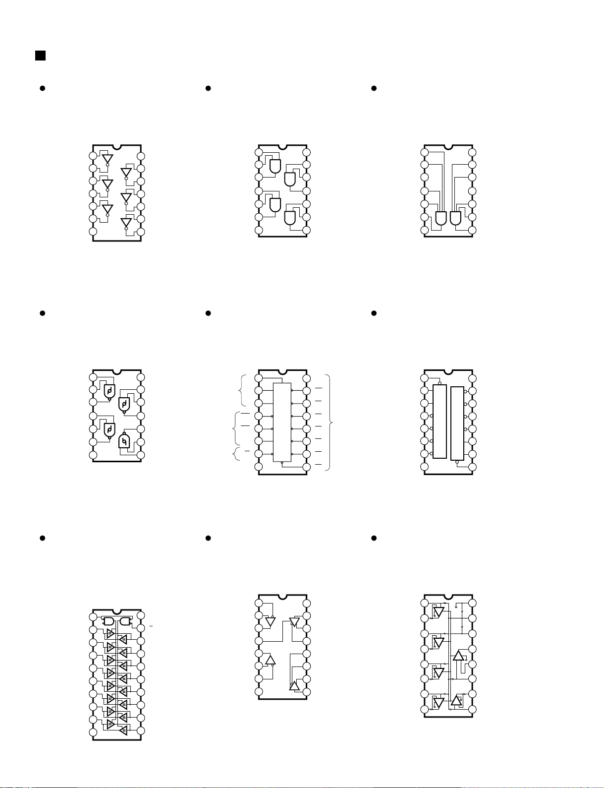
SN74HCU04NSR (XW842A00)
SN74HCU04N (IG142250)
Hex Inverter
DM:
AM:
HD74LV08AFPEL (IS000800)
Quad 2 Input AND
DM: IC101
HD74LV21ATELL (X0010A00)
Dual 4 Input AND
DM: IC310
SN74HC132NSR (XW792A00)
MM74HC132SJX (XY352A00)
Quad 2 Input NAND
DM: IC914
SN74HCT138NSR (XY865A00)
3 to 8 Demultiplexer
DM: IC600
HD74LVC139FPEL (XS048A00)
Dual 2 to 4 Demultiplexer
DM: IC308
HD74LV245ATELL (XW744A00)
74LVC245APW (XZ286A00)
TC74VHCT245AFT (XT744A00)
Octal 3-State Bus Transceiver
DM: IC103, 104, 301-303, 304-306, 911
SN75C1168N (XU463A00)
Line Driver/Receiver
AM: IC307
M5227P (XF751A00)
5-Band Graphic Equalizer
AM: IC104, 105
IC510, 511
IC301
1
2
3
1A
1Y
4
2A
5
2B
6
2Y
VSS
7
1B
14
13
12
VDD
4A
11
4Y
10
3B
9
3A
8
3Y
4B
1
2
3
1A
NC
4
1C
5
1D
6
1Y
7
GND
1B
14
13
12
Vcc
2C
11
NC
10
2B
9
2A
8
2Y
2D
1
2
3
1A
1Y
4
2Y
5
2A
6
2B
7
GND
1B
14
13
12
VDD
4A
11
4Y
10
3Y
9
3B
8
3A
4B
1
2
3
4
5
6
7
A
B
C
G2A
G2B
G1
Y7 Y5
Y4
Y3
Y2
Y1
Y0
Y6
16
15
14
13
12
11
10
8
9
Enable
Output
Output
Select
A
B
C
G2A
G2B
Y7
GND
G1
Vcc
YO
Y1
Y2
Y3
Y5
Y6
Y4
1
2
3
4
5
6
7
1G
1A
1B
1Y0
1Y1
1Y2
1Y3
A
G
B
Y0
Y1
Y2
Y3
16
15
14
13
12
11
10
Vcc
2G
2A
2B
2Y0
2Y1
2Y2
8
GND
9
2Y3
Y2
Y3
Y1
Y0
B
A
G
1
2
3
4
5
6
7
20
19
18
17
16
15
14
Vcc
G
B1
B2
B3
B4
B5
B6
B7
B8
8
9
10
12
11
GND
A8
A7
A6
A5
A4
A3
A2
A1
D1R
13
1
2
3
4
5
6
7
1B
1A
1R
1DE
2R
2A
2B
16
15
14
13
12
11
10
Vcc
1D
1Y
1Z
2DE
2Z
2Y
8
GND
9
2D
1
2
3
4
5
6
7
IN1
NF1
IN2
NF2
IN3
NF3
IN4
16
15
14
13
12
11
10
-Vcc
GND
+Vcc
OUT
-IN
10k
10k
47k
47k
47k540
540
540
540
540
540
47k
47k
47k
+IN
NF5
8
NF4
9
IN5
+-
+-
+-
+-
+-
+-
PSR-1000/PSR-2000
20
IC BLOCK DIAGRAM
Page 21
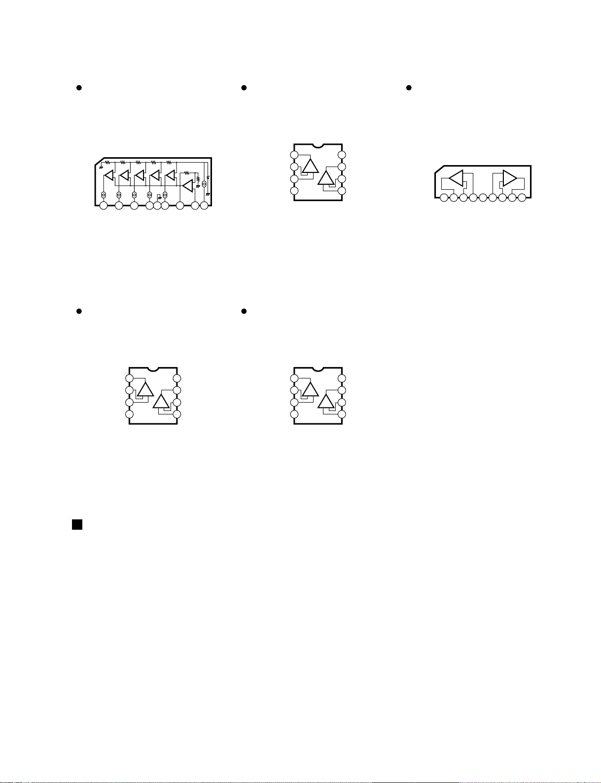
1 2
8
9
VC1
VC2
VCC
In
7
Amp OutGND
4
VC4
3
VC3
-
+
6
VC5
5
+
-
amp
-+-+-+-
+
LB1443N (XF483A00)
LED Driver
AM: IC109 (PSR-2000 only)
M5233FP-600D (X0506A00)
Comparator
DM: IC913
µPC4570HA (XB247A00)
Dual Operational Amplifier
AM: IC100, 102, 103, 107, 108, 111, 112
µPC4572G2-T1 (XF634A00)
Dual Operational Amplifier
DM: IC701
µPC4570G2 (XF291A00)
Dual Operational Amplifier
DM: 702, 703
1A2 3 4 5 6 7 8 9
+V -IN -V
+INOUT
AAA
+V-IN
+IN OUT
BBB
-
+
B
-
+
1
2
3
4-V
8
7
6
5
Output A +V
Non-Inverting
Input A
-DC Voltage Supply
+DC Voltage
Supply
Output B
Inverting
Input B
Non-Inverting
Input B
Inverting
Input A
+-
+-
1
2
3
4-V
8
7
6
5
Output A +V
Non-Inverting
Input A
Ground
+DC Voltage
Supply
Output B
Inverting
Input B
Non-Inverting
Input B
Inverting
Input A
+-
+-
1
2
3
4-V
CH1
8
7
6
5
Output1
+V
CH2
-DC Voltage Supply
Inverting
Input 1
Non-Inverting
Input 1
+DC Voltage Supply
Non-Inverting
Input 2
Output2
Inverting
Input 2
+-
+-
PSR-1000/PSR-2000
CIRCUIT BOARDS CONTENTS
AM (X0189C0) ···················································· 34
DM (X0128C0) (PSR-1000)··························· 22/23
DM (X0129C0) (PSR-2000)··························· 24/25
ENC (X0268B0) ············································· 27/28
HP (X0189C0)····················································· 36
INV (XW193B0)··················································· 35
MK-H (XR565B0)················································ 38
MK-L (XR564B0)················································· 37
MKS5F (X2002A0)·············································· 37
Note: See parts list for details of circuit board component parts.
MOD (X0269B0) (PSR-2000 only)················· 31/32
PB1 (X0269B0) (PSR-2000)·························· 30/33
PB2 (X0269B0) (PSR-1000)·························· 30/33
PN1 (X0268B0)·············································· 26/28
PN2 (X0268B0)·············································· 26/29
PN3 (X0269B0)·············································· 30/32
PN4 (X0269B0)·············································· 30/33
SW (X0189C0)···················································· 36
VR (X0189C0)····················································· 34
21
Page 22
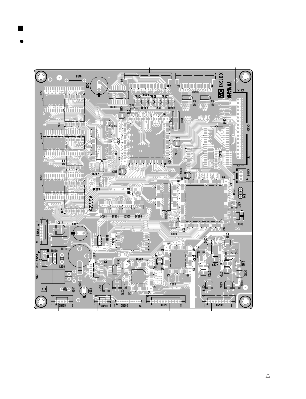
Component side
DM Circuit Board (PSR-1000)
to PN1-CN1
to FDD
to MKS5F-CN1 to INV-CN1
to AM-CN303
to FDDto PN1-CN2
to LCD to AM-CN300 to AM-CN103to AM-CN106
PSR-1000/PSR-2000
22
2NA-V763770-1
1
CIRCUIT BOARDS
Page 23
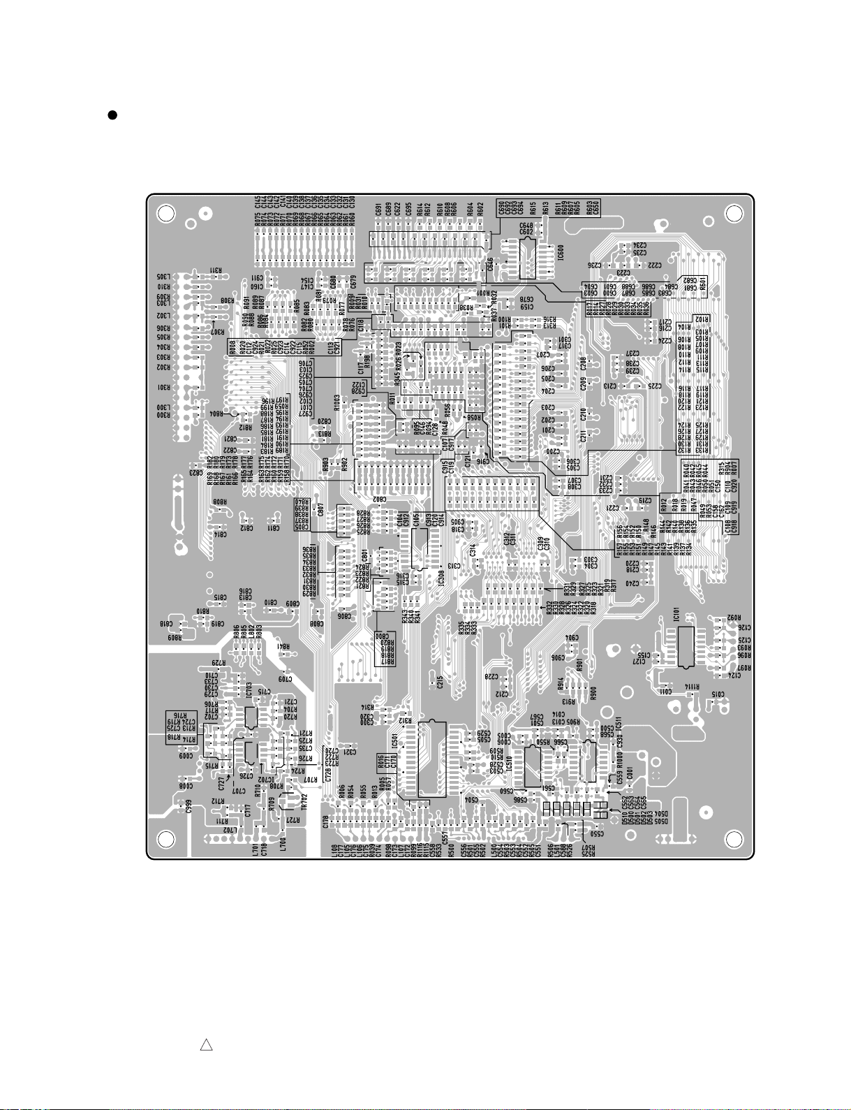
Pattern side
DM Circuit Board (PSR-1000)
PSR-1000/PSR-2000
23
2NA-V763770-2
1
Page 24
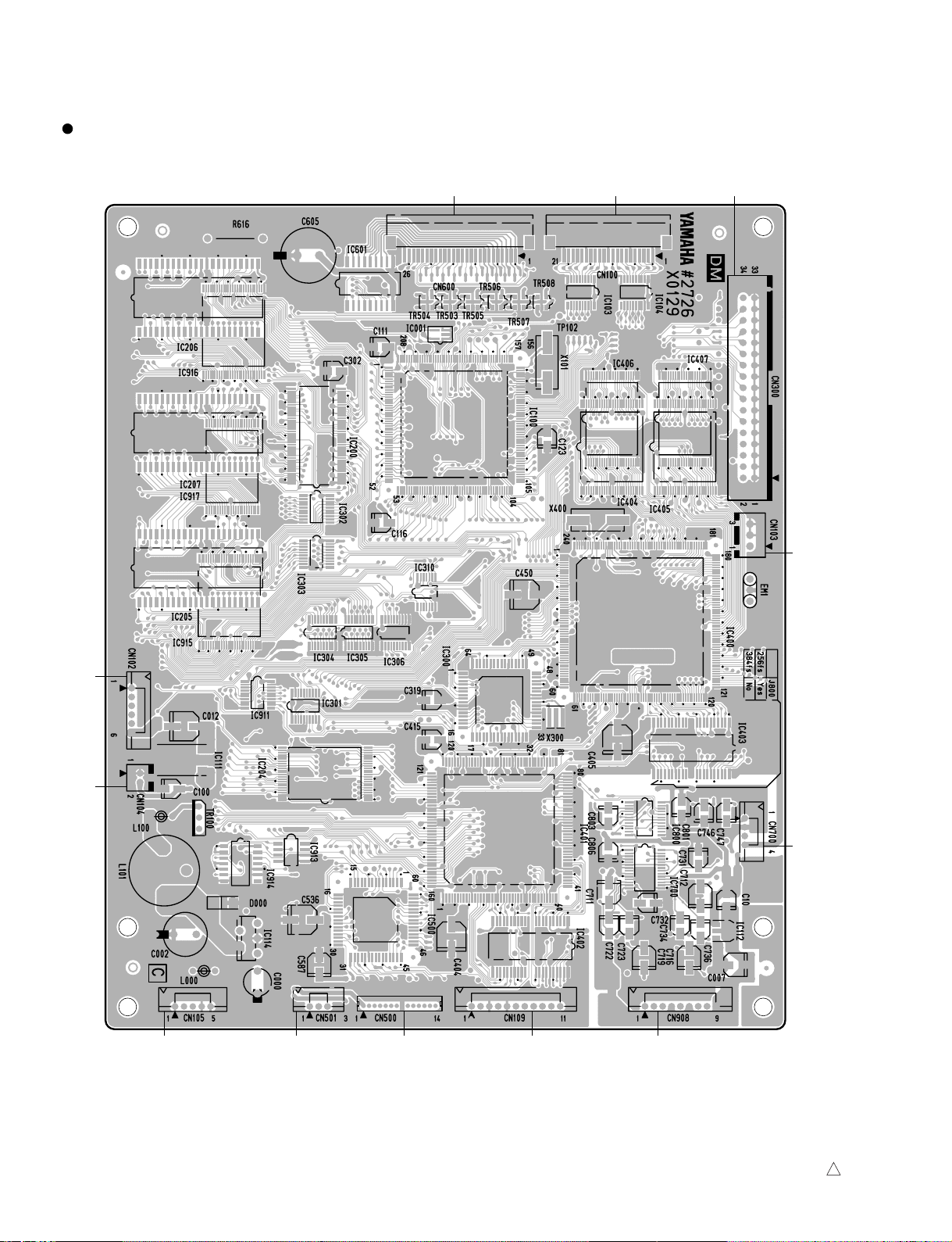
Component side
to PN1-CN1
DM Circuit Board (PSR-2000)
to FDD
to MKS5F-CN1 to INV-CN1
to AM-CN101 (PSR-2000 only)
to PN1-CN2 to FDD
to AM-CN103to AM-CN300to LCDto AM-CN106 to AM-CN303
PSR-1000/PSR-2000
24
2NA-V763780-1
1
Page 25
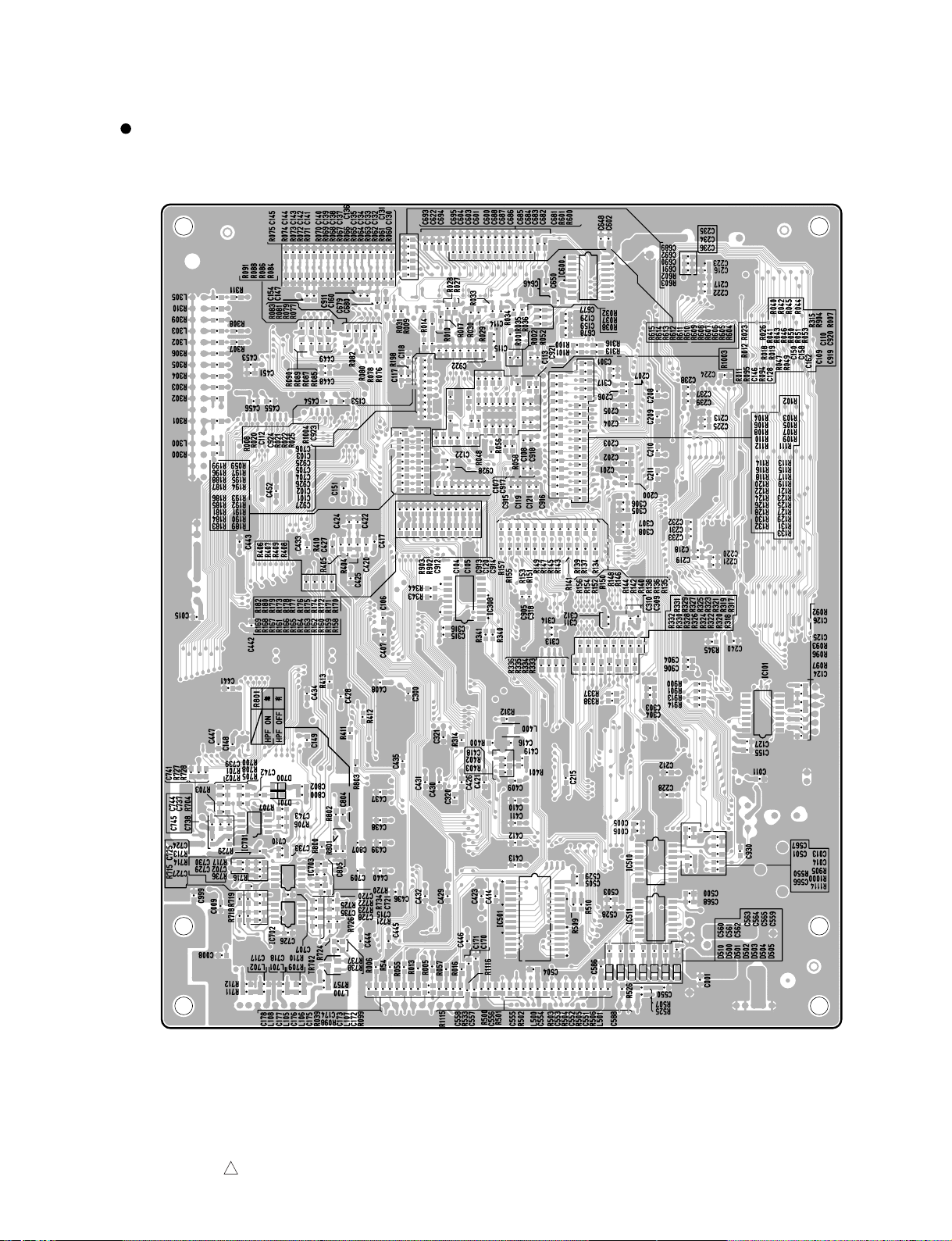
Pattern side
DM Circuit Board (PSR-2000)
PSR-1000/PSR-2000
25
2NA-V763780-2
1
Page 26
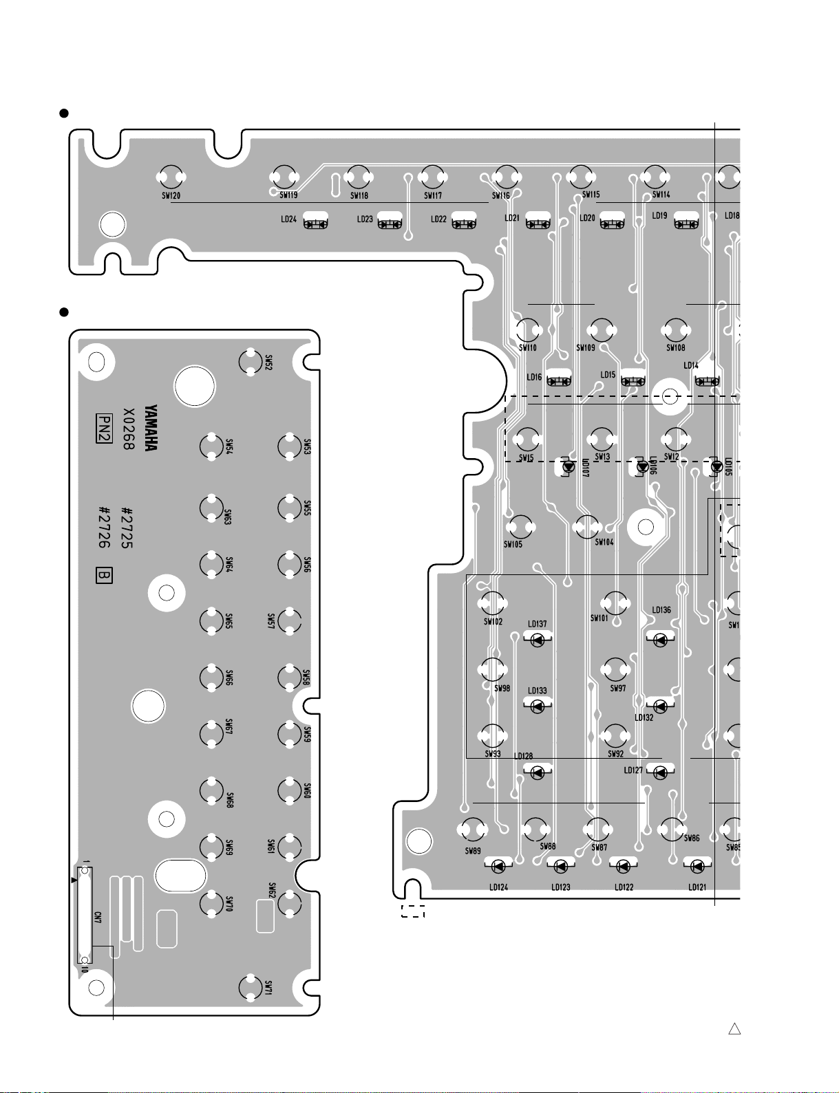
Component side
PN1 Circuit Board
PN2 Circuit Board
A'
A
234
2345678MEMORY
REGISTRATION MEMORY
ONE TOUCH SETTING
ORG
FLUT
UPPER
OCTAVE -
UPPER
OCTAVE +
SYNTH.
CHOI
PA
XG
BRASS BASW.WIND
ORGAN &
ACCORDION
E.PIA
PERCUSSION
VARIATION
DSP MONO SUSTA
HARMONY/EC.
VOCAL
HARMONYTALK MEFFECT
DIRECT
ACCESS
BALAMCE
CHANNEL
ON/OFF
1
(UP)
1
(DOWN)
2
(UP)
2
(DOWN)
3
(UP)
3
(DOWN)
4
(UP)
4
(DOWN)
5
(UP)
5
(DOWN)
6
(UP)
6
(DOWN)
7
(UP)
7
(DOWN)
8
(UP)
EXIT
8
(DOWN)
MIC.
VOICE
VOICE EFFECT
: PSR-2000 only*
to PN1-CN5
PN1, PN2: 2NA-V756860
1
PSR-1000/PSR-2000
26
Page 27
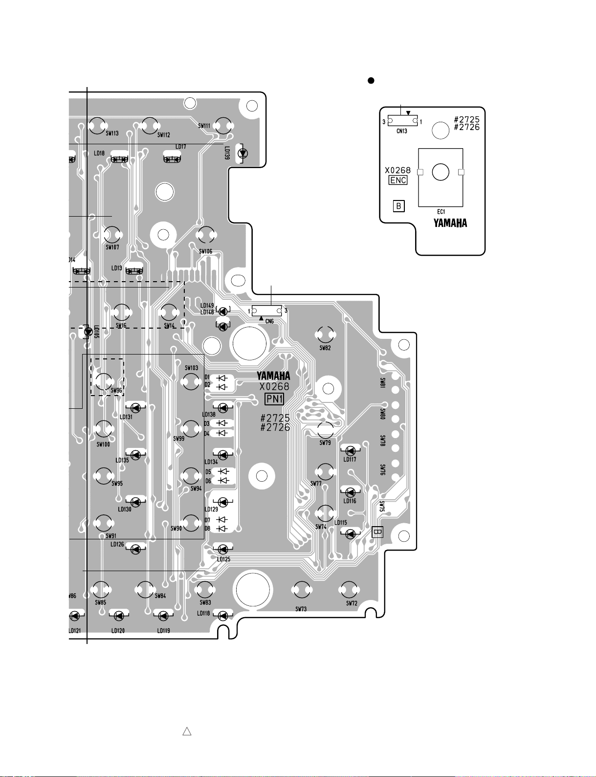
Component side
Component side
to PN1-CN4
ENC Circuit Board
DATA ENTRY
to AM-CN107
(PSR-2000 only)
A'
A
FREEZE1
1 ENTER
2
USER
ORGAN
FLUTES
MUSIC
FINDER
LCD
select J
LCD
select I
LEFT
LAYER
MAIN
NEXT BACK
LCD
select H
LCD
select G
LCD
select F
STRINGS
CHOIR &
PAD
BASS GUITAR
E.PIANO
PIANO &
PARPSI.
SUSTAIN TOUCH
LEFT HOLD
C.
VH TYPE
SELECT
PN1, ENC: 2NA-V756860
1
PSR-1000/PSR-2000
27
Page 28
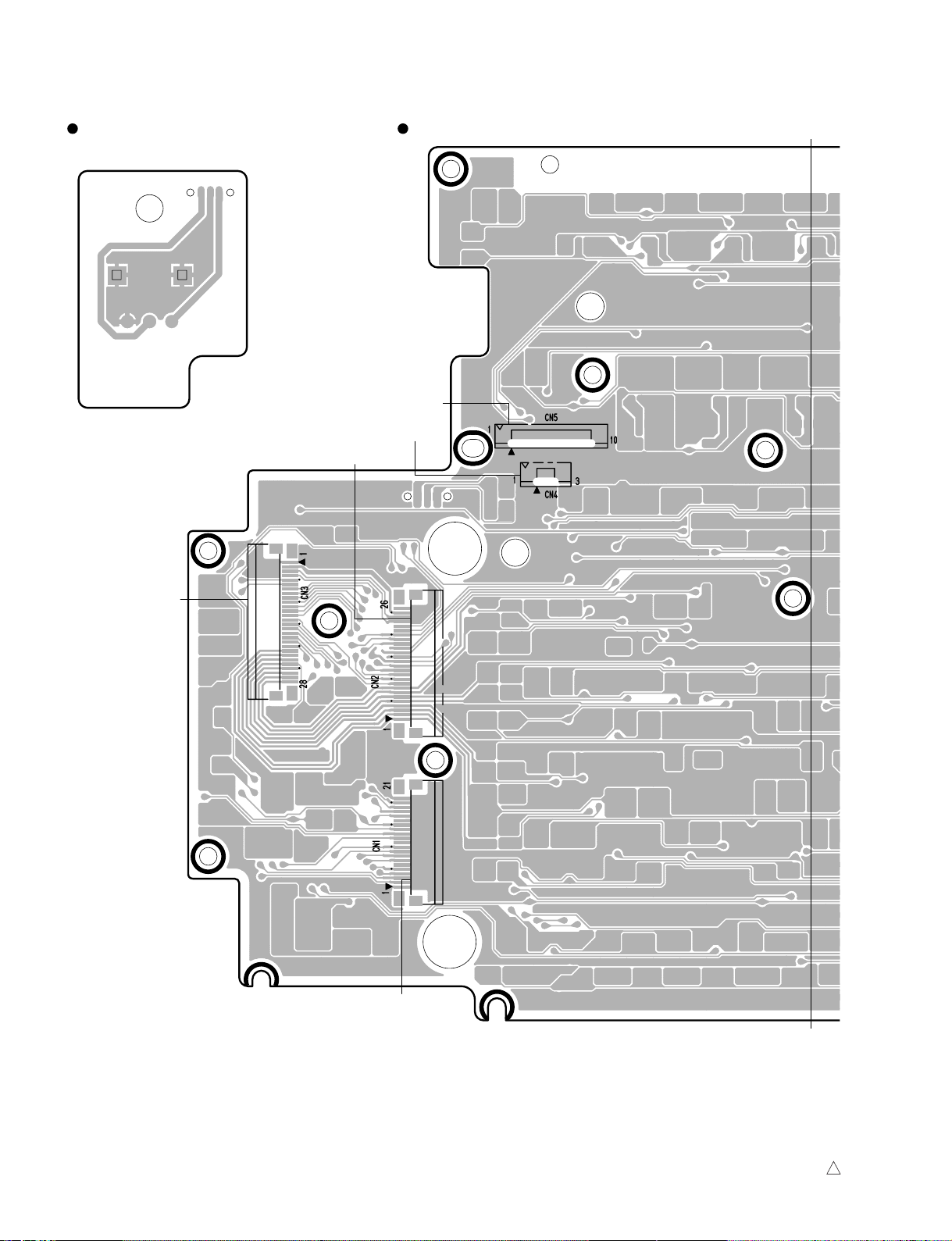
B'
B
Pattern side
to PN2-CN7
ENC Circuit Board PN1 Circuit Board
to ENC-CN13
to PN3-CN8
to DM-CN600
to DM-CN100
PN1, ENC: 2NA-V756860
1
PSR-1000/PSR-2000
28
Page 29
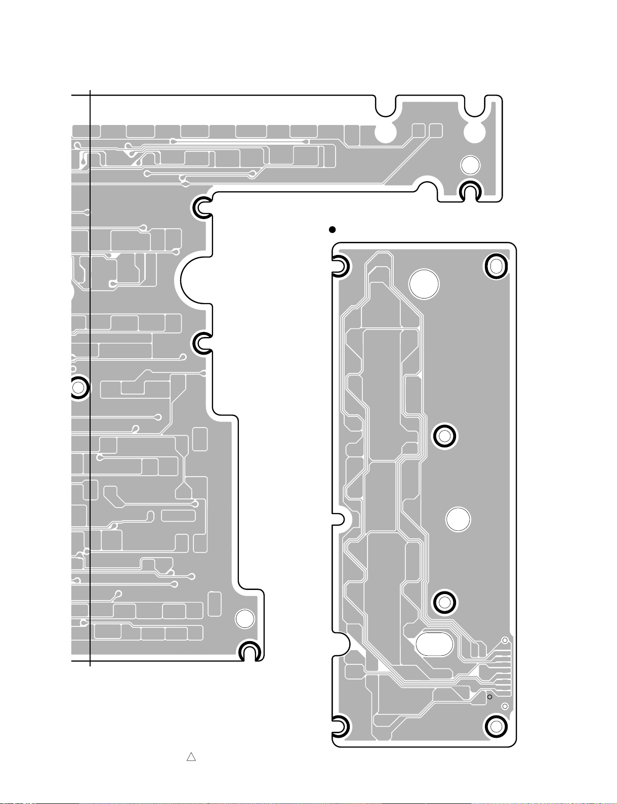
PN2 Circuit Board
B'
B
Pattern side
Pattern side
PN1, PN2: 2NA-V756860
1
PSR-1000/PSR-2000
29
Page 30
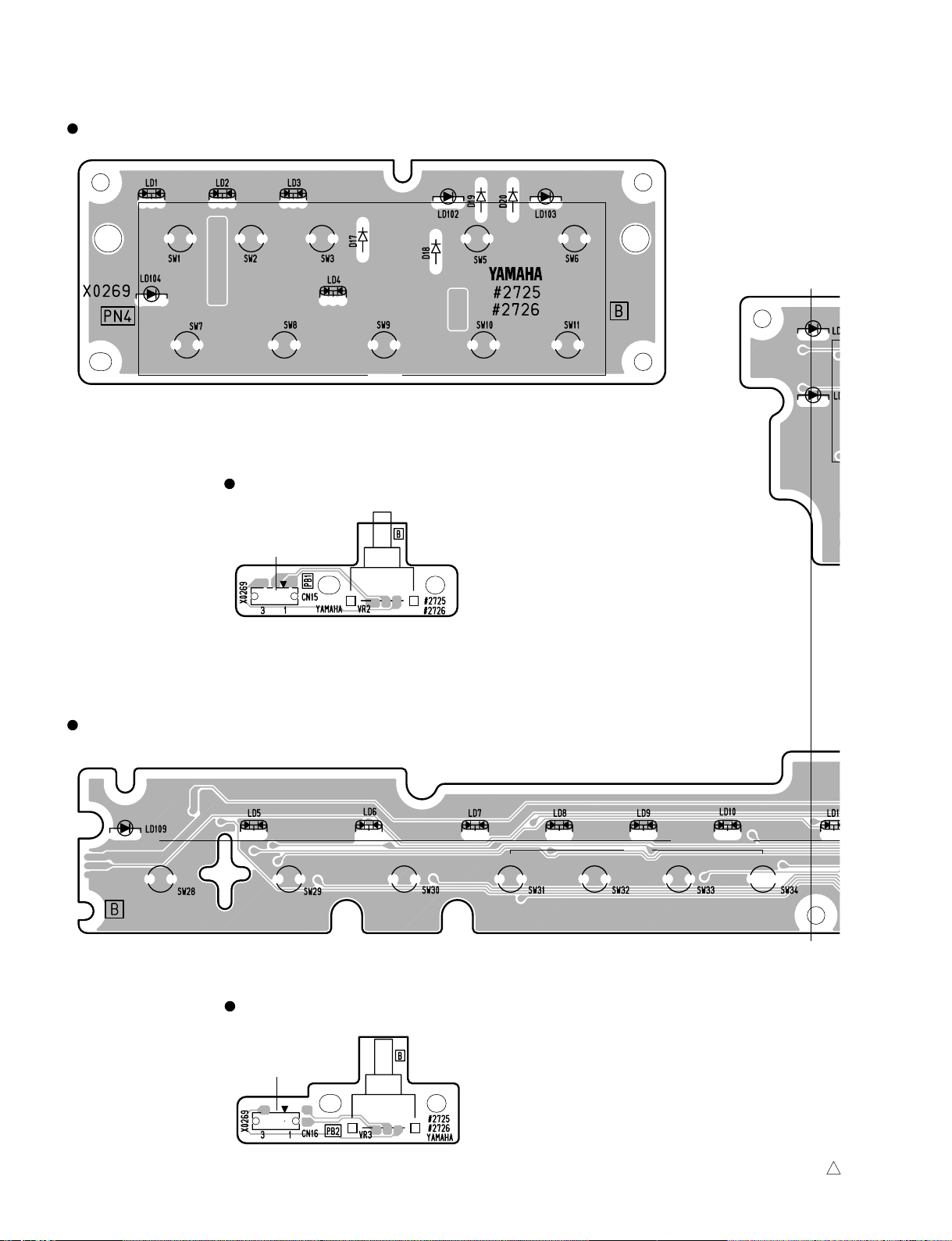
C'
C
Component side
Component side
EXTRA
TRACKS TRACK 2
REC TOP START/STOP
SONG
RW FF
TRACK 1 REPEAT
METRONOME
PN4 Circuit Board
PN3 Circuit Board
PB1 Circuit Board (PSR-2000)
Component side
PB2 Circuit Board (PSR-1000)
to PN3-CN10
PITCH BEND
to PN3-CN10
PITCH BEND
ACMP BREAK INTRO A B C D
MAIN
STYLE CONTROL
P
PN3, PN4, PB1, PB2: 2NA-V756870
1
PSR-1000/PSR-2000
30
Page 31

C'
C
Component side
Component side
MOD Circuit Board (PSR-2000 only)
to PN3-CN11
MODULATION
ENDING/rit.
AUTO
FILL IN
OTS LINK
SYNC. STOP SYNC. START START/STOP
FADE IN/OUT
123
MULTI PAD
STOP
TRANSPOSE - TRANSPOSE + TENPO - TENPO + TAP TENPO
4
SOUND
CREATOR
LCD
select A
LCD
select B
LCD
select C
LCD
select D
LCD
select E
DIGITAL
RECORDING
MIXING
CONSOLE
DEMO
HELP
FUNCTION
POP & ROCK SWING & JAZZ BALLROOM MARCH & WALTZ
BALLAD DANCE
STYLE
LATIN USER
PN3, MOD: 2NA-V756870
1
PSR-1000/PSR-2000
31
Page 32

MOD Circuit Board (PSR-2000 only)
D'
D
PN3 Circuit Board
Pattern side
to PN1-CN3
PN3, MOD: 2NA-V756870
1
PSR-1000/PSR-2000
32
Page 33

PB2 Circuit Board (PSR-1000)
D'
D
PN4 Circuit Board
Pattern side
Pattern side
PB1 Circuit Board (PSR-2000)
Pattern side
Pattern side
to MOD-CN14 (PSR-2000 only)
to PB2-CN16 (PSR-1000)
PB1-CN15 (PSR-2000)
PN3, PN4, PB1, PB2: 2NA-V756870
1
PSR-1000/PSR-2000
33
Page 34

Component side
VR Circuit Board
MASTER VOLUME
E'
E
Component side
LCD
CONTRAST
TO HOST
HOST SELECT MIDI
IN OUT
AM Circuit Board
Mac MIDI
PC1 PC2
to DM-CN908 to DM-CN105to DM-CN501
to DM-CN109
AM, VR: 2NA-V756840
4
PSR-1000/PSR-2000
34
Page 35

: PSR-2000 only*
Component side
INV Circuit Board
to LCD to DM-CN104
F'
F
E'
E
12
FOOT PEDAL
MIC. LINE
INPUT
VOLUME
MIC./
LINE IN
AUX OUT
(LEVEL FIXED)
OUT
RL R
to Speakers
(Tweeter)
to Speakers
(Woofer)
to DM-CN700
(PSR-2000 only)
to PN1-CN6
(PSR-2000 only)
AM: 2NA-V756840
INV: 2NA-V420050
4
PSR-1000/PSR-2000
35
Page 36

F'
F
Component side
Component side
HP Circuit Board
OUT PUT
DC-IN
R L/L+R
PHONES
Component side
SW Circuit Board
STANDBY/ON
AM, HP, SW: 2NA-V756840
4
PSR-1000/PSR-2000
36
Page 37

G'
G
Component side
Component side
to MK-H
to DM-CN102
MK-L Circuit Board
MKS5F Circuit Board
G'
G
H'
H
H'
H
to MK-H
MK-L: 2NA-VV58380
MKS5F: 2NAKZ-V814260
PSR-1000/PSR-2000
37
Page 38

PSR-1000/PSR-2000
38
I'
I
I'
I
J'
J
J'
J
Component side
to MKS5F-CN4
MK-H Circuit Board
to MK-L
MK-H: 2NA-VV583900
Page 39

TEST PROGRAM
PSR-1000/PSR-2000
39
1. Preparation
1) PA-300 (AC adaptor) is used.
2) The volume is usually moved to the use position when no volume change is required.
3) Measuring instruments: frequency counter, level meter (with JIS-C filter)
Note: Connect a stereo plug to the [PHONES] jack at 33 ohms.
4) Jigs: foot switch (FC-4), foot volume (FC-7), MIDI cable, floppy disk (2HD & 2DD), microphone (PSR-2000 only)
2. How to enter the Test Program
While pressing the [C#2], [F2] and [G#2] keys, turn the [STANDBY/ON] switch on.
3. Proceeding through the Teat Program
When the test program is activated, the sign “TEST” is indicated on the LCD display.
Automatically performs RAM BACKUP check when entering test mode.
Select the test program item to be executed by pressing the [TEMPO-] or [TEMPO+] button.
Press the [START/STOP] button to execute testing. When the test result is OK, press the [START/STOP] button to return to the test
item name on display. Proceed to the next test by pressing the [TEMPO-] or [TEMPO+] button. When the test result is OK, an asterisk
(*) is added in front of its item name on display.
When the test result is NG, press the [DEMO] button or the lowest (leftmost) white key on the keyboard to return to the test item name
on display and then turn off the [STANDBY/ON] switch to end the test program.
4. Test program list
No. LCD (initial) Test Function and Judgment criteria
1
2
3
4
5
6
7
9
10
12
15
001: Version
002: ROM Check1
003: RAM Check1
004:Flash Check1
005: Wave ROM Check1
006: Wave RAM Check1
007: FDD Check
009: Effect 2 RAM Check
(PSR-2000 only)
010: Effect 3 RAM Check
012: TG1 Check
015: Pitch Check
Displays each ROM version.
ROM versions are displayed alternately on the LCD.
Checks the ROMs that are connected to the CPU bus.
The test results appear on the LCD. Check the LCD “ROM Check1 OK”
Checks the RAMs that are connected to the CPU bus.
The test results appear on the LCD. Check the LCD “RAM Check1 OK”
Checks the Flash Memories that are connected to the CPU bus.
The test results appear on the LCD. Check the LCD “Flash Check1 OK”
Checks the Wave ROMs.
The test results appear on the LCD. Check the LCD “XG Wave ROM Check OK”
Checks the Wave RAMs.
The test results appear on the LCD. Check the LCD “XG Wave RAM Check OK”
Checks the floppy disk drive unit.
Insert the floppy disks one bye one (2HD or 2DD).
The test will be executed immediately if an FD is inserted in the drive. After completing the test for one FD,
replace it with another to continue the test.
Displays “FDD Check OK” if the test result is OK.
Displays “NO FD” and stands by for FD insertion if an FD is drawn out before completion of the test.
Displays “PROTECT FD” if the write-protect switch of FD is on.
Displays “UNFORMAT FD” if non-formatted FD is inserted.
Checks the VOP3 RAM.
Outputs the sine wave (C3) MAX at the send level and MIN at the drive level.
Check the sound by hearing that there is not noise or abnormal sound.
Checks the XG1 RAM.
Outputs the sine wave (C3) MAX at the send level and MIN at the drive level.
Check the sound by hearing that there is not noise or abnormal sound.
Sequentially outputs the sine wave starting from the low keys (from C2 to G4) by switching the channel of the
sound source.
Check the sound by hearing that there is not noise or abnormal sound.
Pitch check: Connect the frequency counter to the [PHONES] jack (33 ohm load).
Outputs the sine wave at 440.0 Hz +/- 0.22 Hz. (PAN = Center)
Decline quantity check of the volume: Connect the level meter (with JIS-C filter) to the [PHONES] jack. Set the
[MASTER VOLUME] at MIN and check the output level.
PHONES L, R: less than -80.0 dBm
Page 40

PSR-1000/PSR-2000
40
No. LCD (initial) Test Function and Judgment criteria
16
17
18
19
20
22
23
24
25
26
28
29
31
36
37
38
39
40
41
42
016: Output R Check
017: Output L Check
018: EQ Low Check
019: EQ Mid Check
020: EQ High Check
022: D/A Noise Check
023: SW, LED Check
024:
All Panel LED On Check
025: Red LED On Check
026: Green LED On Check
028: All LCD On Check
029: All LCD Off Check
031: LCD Brightness Check
036: Pedal 1 Check
037: Pedal 2 Check
038:
Pitch Bend Wheel Check
039:
Modulation Wheel Check
(PSR-2000 only)
040: MIDI Check
041: TO HOST Check
042: MIC Check
(PSR-2000 only)
Connect the level meter (with a JIS-C filter) to each terminal (PHONES, OUTPUT L/L+R, R, AUX OUT L, R).
Set the [MASTER VOLUME] at MAX and check the R channel output level. (1 kHz sine wave, PAN=R)
(PHONES L, R: 33 ohm load OUTPUT L/L+R, R: 10 kohm load AUX OUT L, R: 10 kohm load)
PHONES L: less than -30.0 dBm PHONES R: +3.5 dBm +/-2 dB
OUTPUT L/L+R: less than -50.0 dBm OUTPUT R: +13.5 dBm +/- 2 dBm (PSR-1000), +11.6 dBm +/-2 dBm (PSR-2000)
AUX OUT L: less than -60.0 dBm AUX OUT R:
+9.1 dBm +/- 2 dB (PSR-1000), +5.5 dBm +/- 2 dB (PSR-2000)
Connect the level meter (with a JIS-C filter) to each terminal (PHONES, OUTPUT L/L+R, R, AUX OUT L, R).
Set the [MASTER VOLUME] at MAX and check the L channel output level. (1 kHz sine wave, PAN=L)
(PHONES L, R: 33 ohm load OUTPUT L/L+R, R: 10 kohm load AUX OUT L, R: 10 kohm load)
PHONES L: +3.5 dBm +/- 2 dB PHONES R: less than -30.0 dBm
OUTPUT L/L+R: +13.5 dBm +/- 2 dBm (PSR-1000), +11.6 dBm +/- 2 dBm (PSR-2000) OUTPUT R: less than -50.0 dBm
AUX OUT L:
+9.1 dBm +/- 2 dB (PSR-1000), +5.5 dBm +/- 2 dB (PSR-2000)
AUX OUT R: less than -60.0 dBm
Check the sine wave output of EQ-Low frequency at about 65.4 Hz (C1). (PAN=Center)
Check the sine wave output of EQ-Mid frequency at about 523 Hz (C4). (PAN=Center)
Check the sine wave output EQ-High frequency at about 4186 Hz (C7). (PAN=Center)
Checks D/A converter noise.
Connect the level meter (with a JIS-C filter) to each terminal (PHONES, OUTPUT L/L+R, R, AUX OUT L, R) .
Set the [MASTER VOLUME] at MAX and check the noise level.
PHONES L, R: less than -75.0 dBm OUTPUT L/L+R, R: less than -70.0 dBm AUX OUT L, R: less than -70.0 dBm
Check the switches on the panel and LED.
Press the switches on the LCD as instructed. A pre-assigned note is output when the switch is pressed. (See table
1). When the switch with LED is pressed, that LED will light up. As the check result appears on the LCD when
all the switches are pressed as instructed. Check that OK is displayed. For the dial check, confirm that the
turning the data dial clockwise will increase the numerical value from 50 to 100 and turning it counterclockwise
will reduce it from 100 to 0.
Check that all panel LEDs are on. (Except for the [MIC. OVER] and [MIC. SIGNAL] LEDs of PSR-2000)
The 2-colors LED light up in orange.
Check that all red LEDs are on. (Except for the [MIC. OVER] LED of PSR-2000)
The 2-colors LED light up in red.
Check that all green LEDs are on. (Except for the [MIC. SIGNAL] LED of PSR-2000)
The 2-colors LED light up in green.
Check that all LCD dots are on.
Check that all LCD dots are off.
Press the [1] to [4] switches of [ONE TOUCH SETTING] in order. The brightness of the LCD grows lighter
every time a switch is pressed.
Connect the foot switch (FC-4) to the [FOOT PEDAL 1] jack.
Check that the C3 note is output when pressing the pedal, and that the C4 note is output when releasing the pedal .
Connect the foot volume (FC-7) to the [FOOT PEDAL 2] jack.
Check that the C3 note is output when fully pressing the pedal to the back (to maximum), and that the C4 note is
output when fully pressing the pedal to the front (to minimum).
Checks the pitch bend wheel.
First, it is checked that the [PITCH BEND] wheel is a center position.
Check that the C3 note is output when rotating the [PITCH BEND] wheel to minimum from center, and that the
C4 note is output when rotating it to maximum.
Checks the modulation wheel.
First, it is checked that the [MODULATION] wheel is a center position.
Check that the C3 note is output when rotating the [MODULATION] wheel to minimum from center, and that
the C4 note is output when rotating it to maximum.
After connecting the [MIDI IN] jack and [MIDI OUT] jack with a MIDI cable, execute the test. Set the [HOST
SELECT]switch to “MIDI”.
Check that the C4 note is output and that the LCD displays “OK”. If there is no input after one second since
signal output, it is judged NG.
Connect pin 3 to pin 5 and pin 6 to pin 8 of the [TO HOST] terminal, and execute the test.
Check that the following note sounds when changing the [HOST SELECT] switch position according to the
LCD indication; the LCD will display “OK”. (PC1: note C3; PC2: note C4; MAC: note C5) If there is no input
after one second since signal output, it is judged NG.
Connect a microphone to the [MIC./LINE IN] jack and speak to it.
Set the [MIC./LINE] select switch to [MIC.] and set the [INPUT VOLUME] at maximum.
Check the voice sound by hearing that there is not unusual noise or abnormal sound.
Page 41

PSR-1000/PSR-2000
41
No. LCD (initial) Test Function and Judgment criteria
43
44
45
46
47
55
56
043: ROM Check2
044: RAM Check2
045: Flash Check2
046: Wave ROM Check2
047: Wave RAM Check2
055: Factory Set
056: Test Exit
Checks the ROMs that are connected to the CPU bus.
Check the LCD “ROM Check2 OK”
Checks the RAMs that are connected to the CPU bus.
Check the LCD “RAM Check2 OK”
Checks the Flash Memories that are connected to the CPU bus.
Check the LCD “Flash Check2 OK”
Checks the Wave ROMs.
Check the LCD “XG Wave ROM Check OK”
Checks the Wave RAMs.
Check the LCD “XG Wave RAM Check OK”
All the RAMs are initialized and set to the factory preset data when executing this test.
Exit from the test program after executing this test.
• Power On Reset
All the RAMs are initialized and set to the factory preset data when the [STANDBY/ON] switch is turned on while pressing the
highest (rightmost) white key on the keyboard.
Note: 0 dBm=0.775 V
Time is required to complete the checks performed by test No. 43–47.
• TABLE 1
ORDER SWITCH
NOTE (PSR-1000)
1
2
3
4
5
6
7
8
9
10
11
12
13
14
15
16
17
18
19
20
21
22
23
24
25
26
27
28
29
30
31
32
33
34
35
36
37
38
39
40
EXTRA TRACKS
TRACK2
TRACK1
REPEAT
METRONOME
REC
TOP
START/STOP (SONG)
RW
FF
8BEAT
16BEAT
SWING & JAZZ
R & B
DANCE
LATIN
MARCH &WALTZ
USER STYLE
TRANSPOSE TRANSPOSE +
TEMPO TEMPO +
TAP TEMPO
PAD STOP
FADE IN/OUT
PAD1
PAD2
PAD3
PAD4
ACCOMP. ON/OFF
BREAK
INTRO
MAIN A
MAIN B
MAIN C
MAIN D
ENDING
AUTO FILL
OTS LINK
SYNC STOP
C2
C#2
D2
D#2
E2
F2
F#2
G2
G#2
A2
A#2
B2
C3
C#3
D3
D#3
E3
F3
F#3
G3
G#3
A3
A#3
B3
C4
C#4
D4
D#4
E4
F4
F#4
G4
G#4
A4
A#4
B4
C5
C#5
D5
D#5
NOTE (PSR-2000)
C2
C#2
D2
D#2
E2
F2
F#2
G2
G#2
A2
A#2
B2
C3
C#3
D3
D#3
E3
F3
F#3
G3
G#3
A3
A#3
B3
C4
C#4
D4
D#4
E4
F4
F#4
G4
G#4
A4
A#4
B4
C5
C#5
D5
D#5
ORDER SWITCH
NOTE (PSR-1000)
41
42
43
44
45
46
47
48
49
50
51
52
53
54
55
56
57
58
59
60
61
62
63
64
65
66
67
68
69
70
71
72
73
74
75
76
77
78
79
80
SYNC START
START/STOP (STYLE)
SOUND CREATER
DIGITAL RECORDING
MIXING CONSOLE
DEMO
HELP
FUNCTION
A
B
C
D
E
DIRECT ACCESS
BALANCE
PART ON/OFF
1-U
1-L
2-U
2-L
3-U
3-L
4-U
4-L
5-U
5-L
6-U
6-L
7-U
7-L
8-U
8-L
EXIT
F
G
H
I
J
BACK
NEXT
E5
F5
F#5
G5
G#5
A5
A#5
B5
C6
C2
C#2
D2
D#2
E2
F2
F#2
G2
G#2
A2
A#2
B2
C3
C#3
D3
D#3
E3
F3
F#3
G3
G#3
A3
A#3
B3
C4
C#4
D4
D#4
E4
F4
F#4
NOTE (PSR-2000)
E5
F5
F#5
G5
G#5
A5
A#5
B5
C6
C2
C#2
D2
D#2
E2
F2
F#2
G2
G#2
A2
A#2
B2
C3
C#3
D3
D#3
E3
F3
F#3
G3
G#3
A3
A#3
B3
C4
C#4
D4
D#4
E4
F4
F#4
Page 42

SYSTEM RESET
This operation lets you restore the PSR-1000/2000 to its original factory settings. These settings include System Setup, MIDI Setup, User
Effect, Music Finder, and Files & Folders.
I
F
J
G
H
D
A
E
B
C
8
1 2 3 4 5 6 7
Restores the System Setup parameters to the
original factory settings. You can also restore only
the System Setup settings by simultaneously
holding down the highest key on the keyboard (C6)
and turning on the power.
Restores the MIDI
templates to the original
factory settings.
Restores the User Effects
to the original factory
settings.
Restores the Music Finder
data to the original factory
settings.
Deletes all files and folders
stored in the User page.
Executes the Factory Reset operation
for all items checkmarked above.
These call up the corresponding Open/ Save
displays. These let you store the corresponding
data as files to disk, for future recall. Pressing
each of these buttons calls up the corresponding
Open/Save display, from which you can select
the corresponding PRESET page. From this
PRESET page, you can save the relevant data.
The functions and settings
below do not apply to the
Factory Reset operation.
However, you can restore
these to their original settings by calling up the preset
System Setup files, using
the Open/Save System Files
function.
Language
Owner Name
LCD Brightness
All Music Finder records can
be stored together as a single file. When calling up a
stored file, a message
appears prompting you to
replace or append the
records as desired.
Replace:
All Music Finder records currently in the instrument are
deleted and replaced with
the records of the selected
file.
Append:
The records called up are
added to the vacant record
numbers.
PSR-1000/PSR-2000
42
ORDER SWITCH
NOTE (PSR-1000)
81
82
83
84
85
86
87
88
89
90
91
92
93
94
95
96
97
98
99
100
101
102
103
104
MAIN
LAYER
LEFT
MUSIC FINDER
LEFT HOLD
TOUCH
SUSTAIN
HARMONY ECHO
POLY/MONO
DSP
FAST/SLOW
PIANO &HARPSI
E.PIANO
ORGAN & ACCORDION
PERCCUSION
GUITAR
BASS
BRASS
W.WIND
STRING
CHOIR & PAD
SYNTH
XG
USER
G4
G#4
A4
A#4
B4
C5
C#5
D5
D#5
E5
F5
F#5
G5
G#5
A5
A#5
B5
C6
C2
C#2
D2
D#2
E2
F2
NOTE (PSR-2000)
G4
G#4
A4
A#4
B4
C5
C#5
D5
D#5
E5
F5
F#5
G5
G#5
A5
A#5
B5
C6
C2
C#2
D2
D#2
E2
F2
ORDER SWITCH
NOTE (PSR-1000)
105
106
107
108
109
110
111
112
113
114
115
116
117
118
119
120
121
122
123
124
125
126
127
ORGAN FLUTES (PSR-2000 only)
OCTAVE OCTAVE +
VOCAL HARMONY (PSR-2000 only)
TALK (PSR-2000 only)
EFFECT (PSR-2000 only)
VH TYPE SELECT (PSR-2000 only)
MC. SETUP (PSR-2000 only)
ENTER
OTS1
OTS2
OTS3
OTS4
FREEZE
REGIST1
REGIST2
REGIST3
REGIST4
REGIST5
REGIST6
REGIST7
REGIST8
MEMORY
–
F#2
G2
–
–
–
–
–
G#2
A2
A#2
B2
C3
C#3
D3
D#3
E3
F3
F#3
G3
G#3
A3
A#3
NOTE (PSR-2000)
F#2
G2
G#2
A2
A#2
B2
C3
C#3
D3
D#3
E3
F3
F#3
G3
G#3
A3
A#3
B3
C4
C#4
D4
D#4
E4
Page 43

PSR-1000/PSR-2000
43
TransmittedFunction... Recognized Remarks
Basic
Channel
Note
Number : True voice
Velocity
After
Touch
Pitch Bend
Control
Change
Prog
Change : True #
System Exclusive
Common : Song Pos.
: Song Sel.
: Tune
System : Clock
Real Time : Commands
: All Sound Off
Aux :
Reset All Cntrls
: Local ON/OFF
Mes- : All Notes OFF
sages: Active Sense
: Reset
Notes:
Mode
Default
Changed
Note ON
Note OFF
Key's
Ch's
0,32
1,5,7,10,11
6,38
64,65,66,67
71-74
84
91,93,94
96-97
98-99
100-101
120
121
1 - 16
1 - 16
O 9nH,v=1-127
X 9nH,v=0
X
X
O
O
O
O
O
O
O
X
O
O
X
X
O
O
O
O
O
O
O
O
O
O
O
O
O
0 - 127
**************
X
X
X
O
O
X
X
X
X
O
X
3
X
**************
0 - 127
**************
O
Mode 1: OMNI ON , POLY Mode 2: OMNI ON ,MONO
Mode 3: OMNI OFF, POLY Mode 4: OMNI OFF,MONO
O
1 - 16
1 - 16
O 9nH,v=1-127
X
O
0 - 24 semi
X
O
X
X
X
O
O
O
(120,126-127)
O
(121)
X
O
(123-125)
O
X
3
X
X
0 - 127
0 - 127
O
O
: Yes
X: No
Default
Messages
Altered
YAMAHA [ Portable Keyboard ] Date : 25,Jun 2001
Model PSR-1000/2000 MIDI Implementation Chart Version : 1.00
Bank Select
Data Entry
Sound Controller
Portament Cntrl
Effect Depth
RPN Inc,Dec
NRPN LSB,MSB
RPN LSB,MSB
All Sound Off
Reset All Cntrls
O 0 - 127
MIDI IMPLEMENTATION CHART
Page 44

PSR-1000/PSR-2000
44
MIDI DATA FORMAT
Many MIDI messages listed in the MIDI Data Format are expressed in decimal numbers, binary numbers and hexadecimal numbers. Hexadecimal
numbers may include the letter “H” as a suffix. Also, “n” can freely be defined as any whole number.
To enter data/values, refer to the table below.
• Except the table above, for example 144-159(decimal)/9nH/1001 0000-1001 1111(binary) denotes the Note On Message for each channel
(1-16). 176-191/BnH/1011 0000-1011 1111 denotes the Control Change Message for each channel (1-16). 192-207/CnH/1100 0000-1100
1111 denotes the Program Change Message for each channel (1-16). 240/FOH/1111 0000 denotes the start of a System Exclusive
Message. 247/F7H/1111 0111 denotes the end of a System Exclusive Message.
• aaH (hexidecimal)/0aaaaaaa (binary) denotes the data address. The address contains High, Mid, and Low.
• bbH/0bbbbbbb denotes the byte count.
• ccH/0ccccccc denotes the check sum.
• ddH/0ddddddd denotes the data/value.
Decimal
0
1
2
3
4
5
6
7
8
9
10
11
12
13
14
15
16
17
18
19
20
21
22
23
24
25
26
27
28
29
30
31
Hexadecimal
00
01
02
03
04
05
06
07
08
09
0A
0B
0C
0D
0E
0F
10
11
12
13
14
15
16
17
18
19
1A
1B
1C
1D
1E
1F
Binary
0000 0000
0000 0001
0000 0010
0000 0011
0000 0100
0000 0101
0000 0110
0000 0111
0000 1000
0000 1001
0000 1010
0000 1011
0000 1100
0000 1101
0000 1110
0000 1111
0001 0000
0001 0001
0001 0010
0001 0011
0001 0100
0001 0101
0001 0110
0001 0111
0001 1000
0001 1001
0001 1010
0001 1011
0001 1100
0001 1101
0001 1110
0001 1111
Decimal
32
33
34
35
36
37
38
39
40
41
42
43
44
45
46
47
48
49
50
51
52
53
54
55
56
57
58
59
60
61
62
63
Hexadecimal
20
21
22
23
24
25
26
27
28
29
2A
2B
2C
2D
2E
2F
30
31
32
33
34
35
36
37
38
39
3A
3B
3C
3D
3E
3F
Binary
0010 0000
0010 0001
0010 0010
0010 0011
0010 0100
0010 0101
0010 0110
0010 0111
0010 1000
0010 1001
0010 1010
0010 1011
0010 1100
0010 1101
0010 1110
0010 1111
0011 0000
0011 0001
0011 0010
0011 0011
0011 0100
0011 0101
0011 0110
0011 0111
0011 1000
0011 1001
0011 1010
0011 1011
0011 1100
0011 1101
0011 1110
0011 1111
Decimal
64
65
66
67
68
69
70
71
72
73
74
75
76
77
78
79
80
81
82
83
84
85
86
87
88
89
90
91
92
93
94
95
Hexadecimal
40
41
42
43
44
45
46
47
48
49
4A
4B
4C
4D
4E
4F
50
51
52
53
54
55
56
57
58
59
5A
5B
5C
5D
5E
5F
Binary
0100 0000
0100 0001
0100 0010
0100 0011
0100 0100
0100 0101
0100 0110
0100 0111
0100 1000
0100 1001
0100 1010
0100 1011
0100 1100
0100 1101
0100 1110
0100 1111
0101 0000
0101 0001
0101 0010
0101 0011
0101 0100
0101 0101
0101 0110
0101 0111
0101 1000
0101 1001
0101 1010
0101 1011
0101 1100
0101 1101
0101 1110
0101 1111
Decimal
96
97
98
99
100
101
102
103
104
105
106
107
108
109
110
111
112
113
114
115
116
117
118
119
120
121
122
123
124
125
126
127
Hexadecimal
60
61
62
63
64
65
66
67
68
69
6A
6B
6C
6D
6E
6F
70
71
72
73
74
75
76
77
78
79
7A
7B
7C
7D
7E
7F
Binary
0110 0000
0110 0001
0110 0010
0110 0011
0110 0100
0110 0101
0110 0110
0110 0111
0110 1000
0110 1001
0110 1010
0110 1011
0110 1100
0110 1101
0110 1110
0110 1111
0111 0000
0111 0001
0111 0010
0111 0011
0111 0100
0111 0101
0111 0110
0111 0111
0111 1000
0111 1001
0111 1010
0111 1011
0111 1100
0111 1101
0111 1110
0111 1111
PSR-1000 PSR-2000
Regular Voice
Organ (Organ Flutes) Voice
Mic
Vocal Harmony
Natural Voice
M. Pad (Multi Pad)
O
-
-
-
-
O
O
O
O
O
-
O
O: available
Page 45

PSR-1000/PSR-2000
45
X
O
X
O
X
X
X
X
O
X
X
O
O
O
O
X
X
X
X
X
X
X
X
X
X
X
X
X
X
X
X
X
X
X
X
X
MIDI Events Status byte 1st Data byte 2nd Data byte Corresponding Voice/Part MIDI Reception (respond/ignore) MIDI Transmission (generated data)
Status Data (HEX) Parameter Data (HEX) Parameter
Regular/
Organ
Voice
Mic/Vocal Harmony Natural
Voice
Song Keyboard Style Extra M.Pad Style Song MIDI
O: available
Main
Layer
Left
Panel
(main generation
method)
Upper
Lower
Key Off
Key On
Control
Change
Mode
Message
8nH
9nH
BnH
BnH
(n:Channel
Number)
(n:Channel
Number)
(n:Channel
Number)
(n:Channel
Number)
kk
kk
0
1
5
6
7
10
11
32
38
64
65
66
67
71
72
73
74
84
91
93
94
96
97
98
99
100
101
120
121
123
124
125
126
127
vv
vv
0
64
126
127
0~127
0~127
0~127
0~127
0~127
0~127
0~127
0~127
0~127
0~127
0~127
0~127
0~127
0~127
0~127
0~127
0~127
0~127
0~127
0~127
-
-
0~127
0~127
0~127
0~127
0
0
0
0
0
0~16
0
(00H)
(40H)
(7EH)
(7FH)
(00H...7FH)
(00H...7FH)
(00H...7FH)
(00H...7FH)
(00H...7FH)
(00H...7FH)
(00H...7FH)
(00H...7FH)
(00H...7FH)
(00H...7FH)
(00H...7FH)
(00H...7FH)
(00H...7FH)
(00H...7FH)
(00H...7FH)
(00H...7FH)
(00H...7FH)
(00H...7FH)
(00H...7FH)
(00H...7FH)
-
-
(00H...7FH)
(00H...7FH)
(00H...7FH)
(00H...7FH)
(00H)
(00H)
(00H)
(00H)
(00H)
(00H...10H)
(00H)
Velocity
(0~127)
Key On:
vv=1~127
Key Off: vv=0
Normal
SFX voice
SFX kit
Drum kit
Data
Data
Data
Data
L64...C...R63
Data
Data
Data
Data
0...63,
64...127
(OFF, ON)
0...63,
64...127
(OFF, ON)
0...63,
64...127
(OFF, ON)
-64...0...+63
-64...0...+63
-64...0...+63
-64...0...+63
Key no.
(0~127)
Data
Data
Data
*1
*1
Data
Data
Data
Data
Data
Data
Data
Data
Data
Data
Data
O
O
O
O
O
O
O
O
O
O
O
O
O
O
O
O
O
O
O
O
O
O
O
O
O
O
O
O
O
O
O
O
O
O
O
O
O
(Harmony Channel/
Melody Channel)
O
(Harmony Channel/
Melody Channel)
X
X
X
O
(Harmony Channel/
Melody Channel)
X
X
X
X
O
(Harmony Channel/
Melody Channel)
O
(Harmony Channel/
Melody Channel)
X
X
X
X
X
X
X
X
X
X
X
O
(Harmony Channel/
Melody Channel)
O
(Harmony Channel/
Melody Channel)
O
(Harmony Channel/
Melody Channel)
O
(Harmony Channel/
Melody Channel)
O
(Harmony Channel/
Melody Channel)
O
(Harmony Channel/
Melody Channel)
X
X
O
(Harmony Channel/
Melody Channel)
X
X
X
X
O
O
O
X
X
O
O
O
O
O
O
O
X
O
O
X
X
X
X
X
O
O
X
O
O
X
X
O
O
O
O
O
X
X
X
X
O
O
O
O
O
O
O
O
O
O
O
O
O
O
O
O
O
O
O
O
O
O
O
O
O
O
O
O
O
O
O
O
O
O
O
O
O
O
O
O
O
O
O
O
O
O
O
O
O
O
O
O
O
O
O
O
O
O
O
O
O
O
O
O
O
O
X
O
X
X
X
X
O
O
O
(Main)
O
(Main/
Layer/Left)
O
(Main/
Layer/Left)
O
(Main/
Layer/Left)
O
(Main/
Layer/Left)
O
(Main/
Layer/Left)
O
(Main/
Layer/Left)
O
(Main)
O
(Main/
Layer/Left)
O
(Main/
Layer/Left)
O
(Main/
Layer/Left)
O
(Main/
Layer/Left)
O
(Main/
Layer/Left)
O
(Main/
Layer/Left)
O
(Main/
Layer/Left)
O
(Main/
Layer/Left)
O
(Main/
Layer/Left)
X
O
(Main/
Layer/Left)
O
(Main/
Layer/Left)
O
(Main/
Layer/Left)
X
X
X
X
O
(Main/
Layer/Left)
O
(Main/
Layer/Left)
O
(Main/
Layer/Left)
X
O
(Main/
Layer/Left)
X
X
X
X
O
O
O
O
X
O
O
O
O
O
X
X
X
X
X
O
O
O
X
O
O
O
O
O
O
O
O
O
O
O
X
O
X
X
X
X
O
O
O
O
O
O
O
O
O
O
O
O
O
O
O
O
O
O
O
O
O
O
O
O
O
O
O
O
O
O
X
O
X
X
X
X
X
O
(Keyboard)
O
(Voice)
O
(Wheel *5,
Pedal)
O
(Mixing
Console)
O
(Mixing
Console)
O
(Mixing
Console)
O
(Mixing
Console)
O
(Pedal)
O
(Voice)
O
(Mixing
Console)
O
(Pedal)
O
(Poly/Mono Sw)
O
(Pedal)
O
(Pedal)
O
(Mixing
Console)
O
(Sound
Creator)
O
(Sound
Creator)
O
(Sound
Creator)
O
(Auto Accom-
paniment)
O
(Mixing
Console)
O
(Mixing
Console)
O
(Mixing
Console)
X
X
O
(Sound
Creator)
O
(Sound
Creator)
O
(Mixing
Console)
O
(Mixing
Console)
X
X
X
X
X
X
X
X
O
O
O
O
O
O
O
O
O
O
O
O
O
O
O
O
O
O
O
O
O
O
O
O
O
O
O
O
O
O
O
O
O
O
O
X
O
O
O
X
O
O
O
O
O
X
X
X
X
X
O
O
O
O
X
O
O
O
X
X
O
O
O
O
X
X
X
X
X
X
X
O
O
O
O
O
O
O
O
O
O
O
O
O
O
O
O
O
O
O
O
O
O
O
O
O
O
O
O
O
O
O
O
O
O
O
O
X
X
X
X
X
X
X
X
X
X
X
X
X
X
X
X
X
X
X
X
X
X
X
X
X
X
X
X
X
X
X
X
X
X
X
X
Key no.
(0~127)
Key no.
(0~127)
Bank Select
MSB
Modulation
Portamento
Time
Data Entry
MSB
Main Volume
Panpot
Expression
Bank Select
LSB
Data Entry
LSB
Sustain
(Damper)
Portamento
Sostenuto
Soft Pedal
Harmonic
Content
Release Time
Attack Time
Brightness
Portamento
Control
Effect1 Depth
(Reverb Send
Level)
Effect3 Depth
(Chorus Send
Level)
Effect4 Depth
(Variation
Send Level)
RPN
Increment
RPN
Decrement
NRPN LSB
NRPN MSB
RPN LSB
RPN MSB
All Sound Off
Reset All
Controllers
All Note Off
Omni Off
Omni On
Mono
Poly
(00H)
(01H)
(05H)
(06H)
(07H)
(0AH)
(0BH)
(20H)
(26H)
(40H)
(41H)
(42H)
(43H)
(47H)
(48H)
(49H)
(4AH)
(54H)
(5BH)
(5DH)
(5EH)
(60H)
(61H)
(62H)
(63H)
(64H)
(65H)
(78H)
(79H)
(7BH)
(7CH)
(7DH)
(7EH)
(7FH)
MIDI CHANNEL MESSAGE (1)
Page 46

mm: 00H-40H-7FH (-64...0...+63)
mm: 00H-40H-7FH (-64...0...+63)
mm: 00H-40H-7FH (-64...0...+63)
mm: 00H-40H-7FH (-64...0...+63)
mm: 00H-40H-7FH (-64...0...+63)
mm: 00H-40H-7FH (-64...0...+63)
mm: 00H-40H-7FH (-64...0...+63)
mm: 04H-28H (32...2.0k[Hz])
mm: 1CH-3AH (500...16.0k[Hz])
mm: 00H-40H-7FH (-64...0...+63)
mm: 00H-40H-7FH (-64...0...+63)
mm: 00H-40H-7FH (-64...0...+63)
rr: drum instrument note number
mm: 00H-40H-7FH (-64...0...+63)
rr: drum instrument note number
mm: 00H-40H-7FH (-64...0...+63)
rr: drum instrument note number
mm: 00H-40H-7FH (-64...0...+63)
rr: drum instrument note number
mm: 00H-40H-7FH (-64...0...+63)
rr: drum instrument note number
mm: 00H-40H-7FH (-64...0...+63)
rr: drum instrument note number
mm: 00H-40H-7FH (-64...0...+63)
rr: drum instrument note number
mm: 00H-7FH (0...127)
rr: drum instrument note number
mm: 00H, 01H-40H-7FH (RND,
L63...C...R63)
rr: drum instrument note number
mm: 00H-7FH (0...127)
rr: drum instrument note number
mm: 00H-7FH (0...127)
rr: drum instrument note number
mm: 00H-7FH (0...127)
(Variation Connection=SYSTEM)
mm: 00H, 01H-7FH (OFF, ON)
(Variation Connection=INSERTION)
O
O
O
X
X
X
X
X
X
X
O
X
X
X
X
X
X
X
X
X
X
X
X
X
X
X
X
X
X
X
X
X
X
X
X
X
X
X
X
X
X
X
X
X
X
X
X
X
X
X
X
X
X
X
X
X
X
X
X
X
X
X
X
X
X
X
X
X
X
O
O
O
O
O
O
O
X
X
O
O
O
X
X
X
X
X
X
X
X
X
X
X
O
O
O
X
X
X
X
X
X
X
O
X
X
X
X
X
X
X
X
X
X
X
X
O
(Sound Creator)
O
(Sound Creator)
O
(Sound Creator)
X
X
X
X
X
X
X
O
(Sound Creator)
X
X
X
X
X
X
X
X
X
X
X
X
O
O
O
O
O
X
X
X
X
O
O
O
X
X
X
X
X
X
X
X
X
X
X
O
O
O
X
X
X
X
X
X
X
O
X
O
O
O
O
O
O
O
O
O
O
O
O
O
O
O
O
O
O
O
O
O
O
O
O
O
O
O
O
O
O
O
O
O
O
X
X
X
X
X
X
X
X
X
X
X
X
X
X
X
X
X
X
X
X
X
X
X
O
(Harmony Channel/
Melody Channel)
O
(Harmony Channel/
Melody Channel)
O
(Harmony Channel/
Melody Channel)
X
X
X
X
X
X
X
X
X
X
X
X
X
X
X
X
X
X
X
X
X
X
X
X
X
X
X
X
X
X
X
X
X
X
X
X
X
X
X
X
X
X
X
O
O
O
O
O
O
O
O
O
O
O
O
O
O
O
O
O
O
O
O
O
O
O
NRPN
NRPN Parameter Data Range Corresponding Voice/Part MIDI Reception (respond/ignore) MIDI Transmission (generated data)
MSB LSB Regular/
Organ Voice
Mic/Vocal Harmony Natural
Voice
Song Keyboard Style Extra M.Pad Style Song MIDIMain
Layer
Left
Panel
(main generation
method)
Upper
Lower
Data Entry
MSB LSB
O
O
O
O
O
O
O
O
O
O
O
O
O
(Drum Only)
01H
01H
01H
01H
01H
01H
01H
01H
01H
01H
01H
01H
14H
15H
16H
17H
18H
19H
1AH
1CH
1DH
1EH
1FH
08H
09H
0AH
20H
21H
30H
31H
34H
35H
63H
64H
66H
rrH
rrH
rrH
rrH
rrH
rrH
rrH
rrH
rrH
rrH
rrH
mmH
mmH
mmH
mmH
mmH
mmH
mmH
mmH
mmH
mmH
mmH
mmH
mmH
mmH
mmH
mmH
mmH
mmH
mmH
mmH
mmH
mmH
mmH
--
--
--
--
--
--
--
--
--
--
--
--
--
--
--
--
--
--
--
--
--
--
--
Vibrato Rate
Vibrato Depth
Vibrato Delay
Low Pass Filter Cutoff Frequency
Low Pass Filter Resonance
EQ BASS (*1)
EQ TREBLE (*1)
EQ BASS Frequency (*1)
EQ TREBLE Frequency (*1)
EG Attack Time
EG Decay Time
EG Release
Drum Low Pass Filter Cutoff
Frequency
Drum Low Pass Filter Resonance
Drum EG Attack Rate
Drum EG Decay Rate
Drum Pitch Coarse
Drum Pitch Fine
Drum Level
Drum Pan
Drum Reverb Send Level
Drum Chorus Send Level
Drum Variation Send Level
PSR-1000/PSR-2000
46
X
X
X
O
MIDI Events Status byte 1st Data byte 2nd Data byte Corresponding Voice/Part MIDI Reception (respond/ignore) MIDI Transmission (generated data)
Status Data (HEX) Parameter Data (HEX) Parameter
Regular/
Organ
Voice
Mic/Vocal Harmony Natural
Voice
Song Keyboard Style Extra M.Pad Style Song MIDIMain
Layer
Left
Panel
(main generation
method)
Upper
Lower
Program
Change
Channel
After Touch
Polyphonic
After Touch
Pitch Bend
Change
Realtime
Message
CnH
DnH
AnH
EnH
F8H
FAH
FBH
FCH
FEH
FFH
(n:Channel
Number)
(n:Channel
Number)
(n:Channel
Number)
(n:Channel
Number)
MIDI Clock
Start
Continue
Stop
Active Sens
System
Reset
pp
vv
kk
cc
-
-
-
-
-
-
-
-
vv
dd
-
-
-
-
-
-
-
-
(00H...7FH)
(00H...7FH)
-
-
Data
MSB
-
-
-
-
-
-
O
O
X
O
-
-
-
-
-
-
X
X
X
O
(Harmony Channel/
Melody Channel)
-
-
-
-
-
-
O
X
X
O
-
-
-
-
-
-
O
O
X
O
O (*2)
O (*2)
X
O (*2)
O
X
O
O
X
O
O
(Main)
O
(Main/
Layer/Left)
X
O
(Main/
Layer/Left)
O
X
X
O
O
O
X
O
O
(Voice)
X
X
O
(Wheel Pedal)
O (*3)
O (*4)
X
O (*4)
O
X
O
O
X
O
O
X
X
O
O
O
O
O
X
X
X
X
Voice Number
(0~127)
Data
Key no.
(0~127)
LSB
-
-
-
-
-
-
(00H...7FH)
(00H...7FH)
(00H...7FH)
(00H...7FH)
*1 The data byte is ignored.
*2 Received when the Clock is set to External.
*3 Transmitted when the Clock is set to Internal and Transmit Clock is set to on.
*4 Transmitted when the Transmit Clock is set to on.
*5 PSR-2000 only.
About Mic/Vocal Harmony column:
The relevant parameters are received by the song part designated by the Effect's Harmony Channel Parameter or Melody Parameter.
NRPN MSB: 14H-1FH (for drums) message is accepted as long as the channel is set with a drum voice.
Data Entry LSB: Ignored.
MIDI CHANNEL MESSAGE (2)
Page 47

MIDI PARAMETER CHANGE TABLE
MIDI Parameter Change table (XG SYSTEM)
PSR-1000/PSR-2000
47
0-63, 64-127 (Off, On)
mm: 00H-7FH (0...127)
mm: 00H-7FH (0...127)
mm: 00H-7FH (0...127)
mm: 00H-7FH (0...127)
mm: 00H, 01H-40H-7FH (RND,
L63...C...R63)
mm: 00H, 01H-40H-7FH (RND,
L63...C...R63)
mm: 00H, 01H-40H-7FH (RND,
L63...C...R63)
mm: 00H-40H-7FH (-64...0...+63)
mm: 00H-40H-7FH (-64...0...+63)
mm: 00H-40H-7FH (-64...0...+63)
X
X
X
X
X
X
X
X
X
X
X
X
X
X
X
X
X
X
X
X
X
X
X
X
X
X
X
X
X
X
X
X
X
X
X
X
X
X
X
X
X
X
X
X
X
X
X
X
X
X
X
X
X
X
X
X
X
O
(Vocal Harmony
Type Edit)
O
(Vocal Harmony
Type Edit)
O
(Vocal Harmony
Type Edit)
O
(Vocal Harmony
Type Edit)
O
(Vocal Harmony
Type Edit)
O
(Vocal Harmony
Type Edit)
O
(Vocal Harmony
Type Edit)
O
(Vocal Harmony
Type Edit)
O
(Vocal Harmony
Type Edit)
X
X
X
X
X
X
X
X
X
X
X
X
X
X
X
X
X
X
X
X
X
X
O
O
O
O
O
O
O
O
O
O
O
X
X
X
X
X
X
X
X
X
X
X
O
(Harmony Channel)
O
(Harmony Channel)
O
(Harmony Channel)
O
(Harmony Channel)
O
(Harmony Channel)
O
(Harmony Channel)
O
(Harmony Channel)
O
(Harmony Channel)
O
(Harmony Channel)
O
(Harmony Channel)
O
(Harmony Channel)
X
X
X
X
X
X
X
X
X
X
X
X
X
X
X
X
X
X
X
X
X
X
NRPN (Vocal Harmony)
NRPN Parameter Data Range Corresponding Voice/Part MIDI Reception (respond/ignore) MIDI Transmission (generated data)
MSB LSB Regular/
Organ Voice
Mic/Vocal Harmony Natural
Voice
Song Keyboard Style Extra M.Pad Style Song MIDIMain
Layer
Left
Panel
(main generation
method)
Upper
Lower
Data Entry
MSB LSB
X
X
X
X
X
X
X
X
X
X
X
00H
01H
02H
02H
02H
02H
02H
02H
02H
02H
02H
00H
1AH
10H
11H
12H
20H
21H
22H
30H
31H
32H
mmH
mmH
mmH
mmH
mmH
mmH
mmH
mmH
mmH
mmH
mmH
--
--
--
--
--
--
--
--
--
--
--
Harmony Mute (*2)
Detune Modulation (*2)
Harmony1 Volume (*2)
Harmony2 Volume (*2)
Harmony3 Volume (*2)
Harmony1 Pan (*2)
Harmony2 Pan (*2)
Harmony3 Pan (*2)
Harmony1 Detune (*2)
Harmony2 Detune (*2)
Harmony3 Detune (*2)
mm: 00H-18H (0...+24[semitones])
mm ll : 00H 00H -100[cent]
...
mm ll : 40H 00H 0[cent]
...
mm ll : 7FH 7FH 100[cent]
mm: 28H-40H-58H
(-24...0...+24[semitones])
-
O
O
O
O
X
X
X
X
O
(Main/
Layer/Left)
O
(Main/
Layer/Left)
O
(Main/
Layer/Left)
O
(Main/
Layer/Left)
O
O
O
O
O
O
O
O
O
(Mixing
Console)
O
(Mixing
Console)
X
X
O
O
O
O
O
O
O
O
O
O
O
O
X
X
X
X
O
(Harmony Channel/
Melody Channel)
X
X
O
O
O
O
O
O
O
O
O
RPN
NRPN Parameter Data Range Corresponding Voice/Part MIDI Reception (respond/ignore) MIDI Transmission (generated data)
MSB LSB Regular/
Organ Voice
Mic/Vocal Harmony Natural
Voice
Song Keyboard Style Extra M.Pad Style Song MIDIMain
Layer
Left
Panel
(main generation
method)
Upper
Lower
Data Entry
MSB LSB
O
O
O
O
00H
00H
00H
7FH
00H
01H
02H
7FH
mmH
mmH
mmH
--
--
llH
--
--
Pitch Bend Sensitivity
Fine Tune
Coarse Tune
Null
Data Entry LSB: Ignored.
PSR-1000
PSR-2000
X
O
*1 2Band Part EQ
PSR-1000
PSR-2000
O
O
PSR-1000
PSR-2000
X
O
*2 Vocal Harmony
* Not Received when Receive System Exclusive Message Parameters is set to off.
* Not transmitted when Transmit System Exclusive Message Parmeters is set to on.
O: available
X
X
X
X
X
X
X
X
X
X
X
X
X
X
X
X
X
X
X
X
X
X
O
O
O
(Function)
X
X
X
X
X
X
X
X
X
X
X
X
X
X
X
X
X
X
X
X
O
O
X
O
O
O
O
X
X
X
X
X
X
X
X
X
X
X
X
X
X
O
O
X
O
X
O
O
O
O
X
O
O
O
O
Address
(H)
Parameter Description XG Default
(H)
Corresponding Voice/Part
MIDI Reception (effective or not for each part)
MIDI Transmission (generated data)
Regular/
Organ
Voice
Mic/Vocal Harmony Natural
Voice
Song Keyboard Style Extra M.Pad Style Song MIDIMain
Layer
Left
Panel
(main generation
method)
Size
(H)
Data
(H)
O
O
X
O
O
(Drum only)
O
O
00 00 00
01
02
03
04
05
06
7D
7E
7F
4
1
1
1
1
1
1
00-0F
00-0F
00-0F
00-0F
00-7F
00-7F
28-58
N
00
00
MASTER TUNE
MASTER VOLUME
MASTER ATTENUATOR
TRANSPOSE
DRUM SETUP RESET
XG SYSTEM ON
ALL PARAMETER RESET
-102.4...0...+102.3[cent]
1st bit 3-0 bit 15-12
2nd bit 3-0 bit 11-8
3rd bit 3-0 bit 7-4
4th bit 3-0 bit 3-0
0...127
0...127
-24...0...+24[semitones]
N: Drum setup number
00=XG system ON
00=ON
*Panel setting
value
7F
00
40
-
-
-
TOTAL SIZE 07
Page 48

PSR-1000/PSR-2000
48
MIDI Parameter Change table (SYSTEM INFORMATION)
PSR-1000
PSR-2000
O
O
- - - - X XXXO---
Address
(H)
Parameter Description Corresponding Voice/Part
MIDI Reception (effective or not for each part)
MIDI Transmission (generated data)
Regular/
Organ
Voice
Mic/Vocal Harmony Natural
Voice
Song Keyboard Style Extra M.Pad Style Song MIDIMain
Layer
Left
Panel
(main generation
method)
Size
(H)
Data
(H)
-
01 00 00
...
0D
0E
0F
E
1
1
20-7F
...
20-7F
Model Name 1
...
Model Name 14
NOT USED
NOT USED
32...127(ASCII CHARACTER)
...
32...127(ASCII CHARACTER)
TOTAL SIZE
Transmitted in response to Dump Request. Not received.
10
MIDI Parameter Change table (EFFECT1)
PSR-1000
PSR-2000
O
O
00-7F
00-7F
00-7F
00-7F
00-7F
00-7F
00-7F
00-7F
00-7F
00-7F
00-7F
00-7F
00-7F
01-7F
REVERB TYPE MSB
REVERB TYPE LSB
REVERB PARAMETER 1
REVERB PARAMETER 2
REVERB PARAMETER 3
REVERB PARAMETER 4
REVERB PARAMETER 5
REVERB PARAMETER 6
REVERB PARAMETER 7
REVERB PARAMETER 8
REVERB PARAMETER 9
REVERB PARAMETER 10
REVERB RETURN
REVERB PAN
02 01 00
02
03
04
05
06
07
08
09
0A
0B
0C
0D
2
1
1
1
1
1
1
1
1
1
1
1
1
O
(Mixing Console)
O
(Mixing Console)
O
(Mixing Console
*Depends on
Reverb Type)
O
(Mixing Console
*Depends on
Reverb Type)
O
(Mixing Console
*Depends on
Reverb Type)
O
(Mixing Console
*Depends on
Reverb Type)
O
(Mixing Console
*Depends on
Reverb Type)
O
(Mixing Console
*Depends on
Reverb Type)
O
(Mixing Console
*Depends on
Reverb Type)
O
(Mixing Console
*Depends on
Reverb Type)
O
(Mixing Console
*Depends on
Reverb Type)
O
(Mixing Console)
X
X
X
X
X
X
X
X
X
X
X
X
X
X
O
O
O
O
O
O
O
O
O
O
O
O
O
O
O
O
O
O
O
O
O
O
O
O
O
O
X
X
X
X
X
X
X
X
X
X
X
X
X
O
O
O
O
O
O
O
O
O
O
O
O
O
X
X
X
X
X
X
X
X
X
X
X
X
X
O
O (*Depends on Reverb Type)
O (*Depends on Reverb Type)
O (*Depends on Reverb Type)
O (*Depends on Reverb Type)
O (*Depends on Reverb Type)
O (*Depends on Reverb Type)
O (*Depends on Reverb Type)
O (*Depends on Reverb Type)
O (*Depends on Reverb Type)
O (*Depends on Reverb Type)
O
O
Address
(H)
Parameter Description XG Default
(H)
Corresponding Voice/Part
MIDI Reception (effective or not for each part)
MIDI Transmission (generated data)
Regular/
Organ
Voice
Mic/Vocal Harmony Natural
Voice
Song Keyboard Style Extra M.Pad Style Song MIDIMain
Layer
Left
Panel
(main generation
method)
Size
(H)
Data
(H)
O
O
O
O
O
O
O
O
O
O
O
O
O
Refer to Effect Parameter
List
˝
˝
˝
˝
˝
˝
˝
˝
˝
˝
˝
- dB...0dB...+6dB
(0...96...127)
L63...C...R63
01(=HALL1)
00
Depends on
Reverb Type
Depends on
Reverb Type
Depends on
Reverb Type
Depends on
Reverb Type
Depends on
Reverb Type
Depends on
Reverb Type
Depends on
Reverb Type
Depends on
Reverb Type
Depends on
Reverb Type
Depends on
Reverb Type
40
40
TOTAL SIZE 0E
00-7F
00-7F
00-7F
00-7F
00-7F
00-7F
REVERB PARAMETER 11
REVERB PARAMETER 12
REVERB PARAMETER 13
REVERB PARAMETER 14
REVERB PARAMETER 15
REVERB PARAMETER 16
02 01 10
11
12
13
14
15
1
1
1
1
1
1
O
(Mixing Console
*Depends on
Reverb Type)
O
(Mixing Console
*Depends on
Reverb Type)
O
(Mixing Console
*Depends on
Reverb Type)
O
(Mixing Console
*Depends on
Reverb Type)
O
(Mixing Console
*Depends on
Reverb Type)
O
(Mixing Console
*Depends on
Reverb Type)
X
X
X
X
X
X
O
O
O
O
O
O
O
O
O
O
O
O
X
X
X
X
X
X
O
O
O
O
O
O
X
X
X
X
X
X
O (*Depends on Reverb Type)
O (*Depends on Reverb Type)
O (*Depends on Reverb Type)
O (*Depends on Reverb Type)
O (*Depends on Reverb Type)
O (*Depends on Reverb Type)
Address
(H)
Parameter Description XG Default
(H)
Corresponding Voice/Part
MIDI Reception (effective or not for each part)
MIDI Transmission (generated data)
Regular/
Organ
Voice
Mic/Vocal Harmony Natural
Voice
Song Keyboard Style Extra M.Pad Style Song MIDIMain
Layer
Left
Panel
(main generation
method)
Size
(H)
Data
(H)
O
O
O
O
O
O
Refer to Effect Parameter
List
˝
˝
˝
˝
˝
Depends on
Reverb Type
Depends on
Reverb Type
Depends on
Reverb Type
Depends on
Reverb Type
Depends on
Reverb Type
Depends on
Reverb Type
TOTAL SIZE 06
Page 49

00-7F
00-7F
00-7F
00-7F
00-7F
00-7F
00-7F
00-7F
00-7F
00-7F
00-7F
00-7F
00-7F
01-7F
00-7F
CHORUS TYPE MSB
CHORUS TYPE LSB
CHORUS PARAMETER 1
CHORUS PARAMETER 2
CHORUS PARAMETER 3
CHORUS PARAMETER 4
CHORUS PARAMETER 5
CHORUS PARAMETER 6
CHORUS PARAMETER 7
CHORUS PARAMETER 8
CHORUS PARAMETER 9
CHORUS PARAMETER 10
CHORUS RETURN
CHORUS PAN
SEND CHORUS TO
REVERB
02 01 20
22
23
24
25
26
27
28
29
2A
2B
2C
2D
2E
2
1
1
1
1
1
1
1
1
1
1
1
1
1
O
(Mixing Console)
O
(Mixing Console
*Depends on
Chorus Type)
O
(Mixing Console
*Depends on
Chorus Type)
O
(Mixing Console
*Depends on
Chorus Type)
O
(Mixing Console
*Depends on
Chorus Type)
O
(Mixing Console
*Depends on
Chorus Type)
O
(Mixing Console
*Depends on
Chorus Type)
O
(Mixing Console
*Depends on
Chorus Type)
O
(Mixing Console
*Depends on
Chorus Type)
O
(Mixing Console
*Depends on
Chorus Type)
O
(Mixing Console
*Depends on
Chorus Type)
O
(Mixing Console)
X
X
X
X
X
X
X
X
X
X
X
X
X
X
X
X
O
O
O
O
O
O
O
O
O
O
O
O
O
O
O
O
O
O
O
O
O
O
O
O
O
O
O
O
X
X
X
X
X
X
X
X
X
X
X
X
X
X
O
O
O
O
O
O
O
O
O
O
O
O
O
O
X
X
X
X
X
X
X
X
X
X
X
X
X
X
O
O (*Depends on Chorus Type)
O (*Depends on Chorus Type)
O (*Depends on Chorus Type)
O (*Depends on Chorus Type)
O (*Depends on Chorus Type)
O (*Depends on Chorus Type)
O (*Depends on Chorus Type)
O (*Depends on Chorus Type)
O (*Depends on Chorus Type)
O (*Depends on Chorus Type)
O
O
O
Address
(H)
Parameter Description XG Default
(H)
Corresponding Voice/Part
MIDI Reception (effective or not for each part)
MIDI Transmission (generated data)
Regular/
Organ
Voice
Mic/Vocal Harmony Natural
Voice
Song Keyboard Style Extra M.Pad Style Song MIDIMain
Layer
Left
Panel
(main generation
method)
Size
(H)
Data
(H)
O
O
O
O
O
O
O
O
O
O
O
O
O
O
Refer to Effect Parameter
List
˝
˝
˝
˝
˝
˝
˝
˝
˝
˝
˝
- dB...0dB...+6dB
(0...96...127)
L63...C...R63
- dB...0dB...+6dB
(0...96...127)
41(=CHORUS1)
00
Depends on
Chorus Type
Depends on
Chorus Type
Depends on
Chorus Type
Depends on
Chorus Type
Depends on
Chorus Type
Depends on
Chorus Type
Depends on
Chorus Type
Depends on
Chorus Type
Depends on
Chorus Type
Depends on
Chorus Type
40
40
00
TOTAL SIZE 0F
00-7F
00-7F
00-7F
00-7F
00-7F
00-7F
00-7F
00-7F
00-7F
00-7F
00-7F
00-7F
00-7F
00-7F
00-7F
00-7F
00-7F
00-7F
00-7F
00-7F
VARIATION TYPE MSB
VARIATION TYPE LSB
VARIATION PARAMETER
1 MSB
VARIATION PARAMETER
1 LSB
VARIATION PARAMETER
2 MSB
VARIATION PARAMETER
2 LSB
VARIATION PARAMETER
3 MSB
VARIATION PARAMETER
3 LSB
VARIATION PARAMETER
4 MSB
VARIATION PARAMETER
4 LSB
VARIATION PARAMETER
5 MSB
VARIATION PARAMETER
5 LSB
VARIATION PARAMETER
6 MSB
VARIATION PARAMETER
6 LSB
VARIATION PARAMETER
7 MSB
VARIATION PARAMETER
7 LSB
VARIATION PARAMETER
8 MSB
VARIATION PARAMETER
8 LSB
VARIATION PARAMETER
9 MSB
VARIATION PARAMETER
9 LSB
02 01 40
42
44
46
48
4A
4C
4E
50
52
2
2
2
2
2
2
2
2
2
2
O
(Mixing Console)
O
(Mixing Console
*Depends on
Variation Type)
O
(Mixing Console
*Depends on
Variation Type)
O
(Mixing Console
*Depends on
Variation Type)
O
(Mixing Console
*Depends on
Variation Type)
O
(Mixing Console
*Depends on
Variation Type)
O
(Mixing Console
*Depends on
Variation Type)
O
(Mixing Console
*Depends on
Variation Type)
O
(Mixing Console
*Depends on
Variation Type)
O
(Mixing Console
*Depends on
Variation Type)
X
X
X
X
X
X
X
X
X
X
O
O
O
O
O
O
O
O
O
O
O
O
O
O
O
O
O
O
O
O
X
X
X
X
X
X
X
X
X
X
O
O
O
O
O
O
O
O
O
O
X
X
X
X
X
X
X
X
X
X
O
O (*Depends on Variation Type)
O (*Depends on Variation Type)
O (*Depends on Variation Type)
O (*Depends on Variation Type)
O (*Depends on Variation Type)
O (*Depends on Variation Type)
O (*Depends on Variation Type)
O (*Depends on Variation Type)
O (*Depends on Variation Type)
Address
(H)
Parameter Description XG Default
(H)
Corresponding Voice/Part
MIDI Reception (effective or not for each part)
MIDI Transmission (generated data)
Regular/
Organ
Voice
Mic/Vocal Harmony Natural
Voice
Song Keyboard Style Extra M.Pad Style Song MIDIMain
Layer
Left
Panel
(main generation
method)
Size
(H)
Data
(H)
O
O
O
O
O
O
O
O
O
O
Refer to Effect Parameter
List
˝
˝
˝
˝
˝
˝
˝
˝
˝
˝
˝
˝
˝
˝
˝
˝
˝
˝
˝
05(=DELAY L,
C, R)
00
Depends on
Variation Type
Depends on
Variation Type
Depends on
Variation Type
Depends on
Variation Type
Depends on
Variation Type
Depends on
Variation Type
Depends on
Variation Type
Depends on
Variation Type
Depends on
Variation Type
00-7F
00-7F
00-7F
00-7F
00-7F
00-7F
CHORUS PARAMETER 11
CHORUS PARAMETER 12
CHORUS PARAMETER 13
CHORUS PARAMETER 14
CHORUS PARAMETER 15
CHORUS PARAMETER 16
02 01 30
31
32
33
34
35
1
1
1
1
1
1
O
(Mixing Console
*Depends on
Chorus Type)
O
(Mixing Console
*Depends on
Chorus Type)
O
(Mixing Console
*Depends on
Chorus Type)
O
(Mixing Console
*Depends on
Chorus Type)
O
(Mixing Console
*Depends on
Chorus Type)
O
(Mixing Console
*Depends on
Chorus Type)
X
X
X
X
X
X
O
O
O
O
O
O
O
O
O
O
O
O
X
X
X
X
X
X
O
O
O
O
O
O
X
X
X
X
X
X
O (*Depends on Chorus Type)
O (*Depends on Chorus Type)
O (*Depends on Chorus Type)
O (*Depends on Chorus Type)
O (*Depends on Chorus Type)
O (*Depends on Chorus Type)
O
O
O
O
O
O
Refer to Effect Parameter
List
˝
˝
˝
˝
˝
Depends on
Chorus Type
Depends on
Chorus Type
Depends on
Chorus Type
Depends on
Chorus Type
Depends on
Chorus Type
Depends on
Chorus Type
TOTAL SIZE 06
PSR-1000/PSR-2000
49
Page 50

00-7F
00-7F
00-7F
00-7F
00-7F
00-7F
00-7F
00-7F
00-7F
00-7F
00-7F
00-7F
01-7F
VARIATION PARAMETER
10 MSB
VARIATION PARAMETER
10 LSB
VARIATION RETURN
VARIATION PAN
SEND VARIATION TO
REVERB
SEND VARIATION TO
CHORUS
VARIATION CONNECTION
VARIATION PART
NUMBER
MW VARIATION
CONTROL DEPTH
BEND VARIATION
CONTROL DEPTH
CAT VARIATION
CONTROL DEPTH
AC1 VARIATION
CONTROL DEPTH
AC2 VARIATION
CONTROL DEPTH
54
56
57
58
59
5A
5B
5C
5D
5E
5F
60
2
1
1
1
1
1
1
1
1
1
1
1
O
(Mixing Console
*Depends on
Variation Type)
O
(Mixing Console)
X
X
X
X
O
(Mixing Console)
X
X
X
X
X
X
X
X
X
X
X
X
X
X
X
X
X
O
O
O
O
O
O
O
O
O
O
X
X
O
O
O
O
O
O
O
O
O
O
X
X
X
X
X
X
X
X
X
X
X
X
X
X
O
O
O
O
O
O
O
O
O
O
X
X
X
X
X
X
X
X
X
X
X
X
X
X
O (*Depends on Variation Type)
O
O
O
O
O
O
O
O
O
X
X
Address
(H)
Parameter Description XG Default
(H)
Corresponding Voice/Part
MIDI Reception (effective or not for each part)
MIDI Transmission (generated data)
Regular/
Organ
Voice
Mic/Vocal Harmony Natural
Voice
Song Keyboard Style Extra M.Pad Style Song MIDIMain
Layer
Left
Panel
(main generation
method)
Size
(H)
Data
(H)
O
O
O
O
O
O
O
O
O
O
X
X
˝
˝
- dB...0dB...+6dB
(0...96...127)
L63...C...R63
- dB...0dB...+6dB
(0...96...127)
- dB...0dB...+6dB
(0...96...127)
INSERTION, SYSTEM
Reception: Part1...16(0...15)
Transmission:
Part1...16(0...15)
AD(64)
OFF(127)
-64...0...+63
-64...0...+63
-64...0...+63
-64...0...+63
-64...0...+63
Depends on
Variation Type
40
40
00
00
00
7F
40
40
40
40
40
TOTAL SIZE 21
00-7F
00-7F
00-7F
00-7F
00-7F
00-7F
VARIATION PARAMETER
11
VARIATION PARAMETER
12
VARIATION PARAMETER
13
VARIATION PARAMETER
14
VARIATION PARAMETER
15
VARIATION PARAMETER
16
02 01 70
71
72
73
74
75
1
1
1
1
1
1
O
(Mixing Console
*Depends on
Variation Type)
O
(Mixing Console
*Depends on
Variation Type)
O
(Mixing Console
*Depends on
Variation Type)
O
(Mixing Console
*Depends on
Variation Type)
O
(Mixing Console
*Depends on
Variation Type)
O
(Mixing Console
*Depends on
Variation Type)
X
X
X
X
X
X
O
O
O
O
O
O
O
O
O
O
O
O
X
X
X
X
X
X
O
O
O
O
O
O
X
X
X
X
X
X
O (*Depends on Variation Type)
O (*Depends on Variation Type)
O (*Depends on Variation Type)
O (*Depends on Variation Type)
O (*Depends on Variation Type)
O (*Depends on Variation Type)
O
O
O
O
O
O
Refer to Effect Parameter
List
˝
˝
˝
˝
˝
Depends on
Variation Type
Depends on
Variation Type
Depends on
Variation Type
Depends on
Variation Type
Depends on
Variation Type
Depends on
Variation Type
TOTAL SIZE 06
PSR-1000/PSR-2000
50
MIDI Parameter Change table (MULTI EQ)
PSR-1000
PSR-2000
X
O
X
O
(Mixing Console)
O
(Mixing Console)
O
(Mixing Console)
X
O
(Mixing Console)
O
(Mixing Console)
O
(Mixing Console)
-
O
(Mixing Console)
O
(Mixing Console)
O
(Mixing Console)
-
O
(Mixing Console)
O
(Mixing Console)
O
(Mixing Console)
-
O
(Mixing Console)
O
(Mixing Console)
O
(Mixing Console)
X
X
X
X
X
X
X
X
X
X
X
X
X
X
X
X
X
X
X
X
X
X
X
X
X
X
X
X
X
X
X
X
X
X
X
X
X
O
O
O
O
O
O
O
O
O
O
O
O
O
O
O
O
O
O
X
X
X
X
X
X
X
X
X
X
X
X
X
X
X
X
X
X
O
O
O
O
O
O
O
O
O
O
O
O
O
O
O
O
O
O
X
X
X
X
X
X
X
X
X
X
X
X
X
X
X
X
X
X
O
O
O
O
O
O
O
O
O
O
O
O
O
O
O
O
O
O
Address
(H)
Parameter Description Corresponding Voice/Part
MIDI Reception (effective or not for each part)
MIDI Transmission (generated data)
Regular/
Organ
Voice
Mic/Vocal Harmony Natural
Voice
Song Keyboard Style Extra M.Pad Style Song MIDIMain
Layer
Left
Panel
(main generation
method)
Size
(H)
Data
(H)
O
O
O
O
O
O
O
O
O
O
O
O
O
O
O
O
O
O
02 40 00
01
02
03
04
05
06
07
08
09
0A
0B
0C
0D
0E
0F
10
11
12
13
14
1
1
1
1
1
1
1
1
1
1
1
1
1
1
1
1
1
1
1
1
1
00-04
34-4C
04-28
01-78
00-01
34-4C
0E-36
01-78
34-4C
0E-36
01-78
34-4C
0E-36
01-78
34-4C
1C-3A
01-78
00-01
EQ TYPE
EQ GAIN1
EQ FREQUENCY1
EQ Q1
EQ SHAPE1
EQ GAIN2
EQ FREQUENCY2
EQ Q2
NOT USED
EQ GAIN3
EQ FREQUENCY3
EQ Q3
NOT USED
EQ GAIN4
EQ FREQUENCY4
EQ Q4
NOT USED
EQ GAIN5
EQ FREQUENCY5
EQ Q5
EQ SHAPE5
flat, jazz, pops, rock, classic
-12...0...+12[dB]
32...2.0k[Hz]
0.1...12.0
shelving, peaking
-12...0...+12[dB]
100...10.0k[Hz]
0.1...12.0
-12...0...+12[dB]
100...10.0k[Hz]
0.1...12.0
-12...0...+12[dB]
100...10.0k[Hz]
0.1...12.0
-12...0...+12[dB]
0.5k...16.0k[Hz]
0.1...12.0
shelving, peaking
TOTAL SIZE 05 The MULTI EQ Parameter cannot be reset to its factory setting with XG SYSTEM ON.
Page 51

00-7F
00-7F
00-7F
00-7F
00-7F
00-7F
INSERTION EFFECT
PARAMETER 11
INSERTION EFFECT
PARAMETER 12
INSERTION EFFECT
PARAMETER 13
INSERTION EFFECT
PARAMETER 14
INSERTION EFFECT
PARAMETER 15
INSERTION EFFECT
PARAMETER 16
20
21
22
23
24
25
1
1
1
1
1
1
O
(Mixing Console
*Depends on
Insertion Type)
O
(Mixing Console
*Depends on
Insertion Type)
O
(Mixing Console
*Depends on
Insertion Type)
O
(Mixing Console
*Depends on
Insertion Type)
O
(Mixing Console
*Depends on
Insertion Type)
O
(Mixing Console
*Depends on
Insertion Type)
X
X
X
X
X
X
X
X
X
X
X
X
O
O
O
O
O
O
X
X
X
X
X
X
O
O
O
O
O
O
X
X
X
X
X
X
O (*Depends on Insertion Type )
O (*Depends on Insertion Type )
O (*Depends on Insertion Type )
O (*Depends on Insertion Type )
O (*Depends on Insertion Type )
O (*Depends on Insertion Type )
O
O
O
O
O
O
Refer to Effect Parameter List
˝
˝
˝
˝
˝
TOTAL SIZE 6
00-7F
00-7F
00-7F
00-7F
00-7F
00-7F
00-7F
00-7F
00-7F
00-7F
00-7F
00-7F
00-7F
00-7F
00-7F
00-7F
INSERTION EFFECT
PARAMETER 1 MSB
INSERTION EFFECT
PARAMETER 1 LSB
INSERTION EFFECT
PARAMETER 2 MSB
INSERTION EFFECT
PARAMETER 2 LSB
INSERTION EFFECT
PARAMETER 3 MSB
INSERTION EFFECT
PARAMETER 3 LSB
INSERTION EFFECT
PARAMETER 4 MSB
INSERTION EFFECT
PARAMETER 4 LSB
INSERTION EFFECT
PARAMETER 5 MSB
INSERTION EFFECT
PARAMETER 5 LSB
INSERTION EFFECT
PARAMETER 6 MSB
INSERTION EFFECT
PARAMETER 6 LSB
INSERTION EFFECT
PARAMETER 7 MSB
INSERTION EFFECT
PARAMETER 7 LSB
INSERTION EFFECT
PARAMETER 8 MSB
INSERTION EFFECT
PARAMETER 8 LSB
30
32
34
36
38
3A
3C
3E
2
2
2
2
2
2
2
2
O
(Mixing Console
*Depends on
Insertion Type)
O
(Mixing Console
*Depends on
Insertion Type)
O
(Mixing Console
*Depends on
Insertion Type)
O
(Mixing Console
*Depends on
Insertion Type)
O
(Mixing Console
*Depends on
Insertion Type)
O
(Mixing Console
*Depends on
Insertion Type)
O
(Mixing Console
*Depends on
Insertion Type)
O
(Mixing Console
*Depends on
Insertion Type)
X
X
X
X
X
X
X
X
X
X
X
X
X
X
X
X
O
O
O
O
O
O
O
O
X
X
X
X
X
X
X
X
O
O
O
O
O
O
O
O
X
X
X
X
X
X
X
X
O (*Depends on Insertion Type )
O (*Depends on Insertion Type )
O (*Depends on Insertion Type )
O (*Depends on Insertion Type )
O (*Depends on Insertion Type )
O (*Depends on Insertion Type )
O (*Depends on Insertion Type )
O (*Depends on Insertion Type )
O
O
O
O
O
O
O
O
Refer to Effect Parameter List
˝
˝
˝
˝
˝
˝
˝
˝
˝
˝
˝
˝
˝
˝
˝
O
(Mixing Console)
O
(Mixing Console
*Depends on
Insertion Type)
O
(Mixing Console
*Depends on
Insertion Type)
O
(Mixing Console
*Depends on
Insertion Type)
O
(Mixing Console
*Depends on
Insertion Type)
O
(Mixing Console
*Depends on
Insertion Type)
O
(Mixing Console
*Depends on
Insertion Type)
O
(Mixing Console
*Depends on
Insertion Type)
O
(Mixing Console
*Depends on
Insertion Type)
O
(Mixing Console
*Depends on
Insertion Type)
O
(Mixing Console
*Depends on
Insertion Type)
O
(Mixing Console)
X
X
X
X
X
X
X
X
X
X
X
X
X
X
X
X
X
X
X
X
X
X
X
X
X
X
X
X
X
X
X
X
X
X
X
X
X
X
X
O
O
O
O
O
O
O
O
O
O
O
O
O
O
O
X
X
X
X
X
X
X
X
X
X
X
X
X
X
X
X
X
X
X
O
O
O
O
O
O
O
O
O
O
O
O
O
O
O
X
X
X
X
X
X
X
X
X
X
X
X
X
X
X
X
X
X
X
O
O (*Depends on Insertion Type )
O (*Depends on Insertion Type )
O (*Depends on Insertion Type )
O (*Depends on Insertion Type )
O (*Depends on Insertion Type )
O (*Depends on Insertion Type )
O (*Depends on Insertion Type )
O (*Depends on Insertion Type )
O (*Depends on Insertion Type )
O (*Depends on Insertion Type )
O
O
O
O
X
X
Address
(H)
Parameter Description Corresponding Voice/Part
MIDI Reception (effective or not for each part)
MIDI Transmission (generated data)
Regular/
Organ
Voice
Mic/Vocal Harmony Natural
Voice
Song Keyboard Style Extra M.Pad Style Song MIDIMain
Layer
Left
Panel
(main generation
method)
Size
(H)
Data
(H)
O
O
O
O
O
O
O
O
O
O
O
O
O
O
O
X
X
03 n 00
02
03
04
05
06
07
08
09
0A
0B
0C
0D
0E
0F
10
11
2
1
1
1
1
1
1
1
1
1
1
1
1
1
1
1
1
00-7F
00-7F
00-7F
00-7F
00-7F
00-7F
00-7F
00-7F
00-7F
00-7F
00-7F
00-7F
00-7F
00-7F
00-7F
00-7F
00-7F
00-7F
INSERTION EFFECT TYPE
MSB
INSERTION EFFECT TYPE
LSB
INSERTION EFFECT
PARAMETER 1
INSERTION EFFECT
PARAMETER 2
INSERTION EFFECT
PARAMETER 3
INSERTION EFFECT
PARAMETER 4
INSERTION EFFECT
PARAMETER 5
INSERTION EFFECT
PARAMETER 6
INSERTION EFFECT
PARAMETER 7
INSERTION EFFECT
PARAMETER 8
INSERTION EFFECT
PARAMETER 9
INSERTION EFFECT
PARAMETER 10
INSERTION EFFECT PART
NUMBER
MW INSERTION
CONTROL DEPTH
BEND INSERTION
CONTROL DEPTH
CAT INSERTION
CONTROL DEPTH
AC1 INSERTION
CONTROL DEPTH
AC2 INSERTION
CONTROL DEPTH
Refer to Effect Parameter List
˝
˝
˝
˝
˝
˝
˝
˝
˝
˝
˝
Reception: Part1...16(0...15)
Transmission: Part1...16(0...15)
AD(64)
OFF(127)
-64...0...+63
-64...0...+63
-64...0...+63
-64...0...+63
-64...0...+63
TOTAL SIZE 12
PSR-1000/PSR-2000
51
MIDI Parameter Change table (EFFECT2)
PSR-1000
PSR-2000
X
O
Page 52

00-7F
00-7F
UNIQUE INSERTION
EFFECT EXTERNAL
CONTROL CH1
(HARMONY CHANNEL)
UNIQUE INSERTION
EFFECT EXTERNAL
CONTROL CH1
(MELODY CHANNEL)
14151
1
O (MicSetting)XXXXXOOX
X
O
O
XXXXXXXXXXX
X
X
X
1...16(0...15), OFF(127)
1...16(0...15), OFF(127)
TOTAL SIZE 2
00-7F
00-7F
00-7F
00-7F
00-7F
00-7F
INSERTION EFFECT
PARAMETER 11
Vibrate Depth
INSERTION EFFECT
PARAMETER 12
Vibrate Rate
INSERTION EFFECT
PARAMETER 13
Vibrate DelayI
NSERTION EFFECT
PARAMETER 14
INSERTION EFFECT
PARAMETER 15
INSERTION EFFECT
PARAMETER 16
20
21
22
23
24
25
1
1
1
1
1
1
O (VH Type
Select)
O (VH Type
Select)
O (VH Type
Select)
X
X
X
X
X
X
X
X
X
X
X
X
X
X
X
O
O
O
X
X
X
X
X
X
X
X
X
O
O
O
X
X
X
X
X
X
X
X
X
X
X
X
X
X
X
X
X
X
X
X
X
X
X
X
X
X
X
X
X
X
X
X
X
X
X
X
X
X
X
X
X
X
X
X
X
0...100cent(0...127)
0Hz(0), 0.1...12.7Hz(1...127)
0...2.54sec(0...127)
TOTAL SIZE 6 The SPECIAL EFFECT Parameter cannot be reset to its factory setting with XG SYSTEM ON.
X
X
X
X
X
X
X
X
X
X
X
X
X
X
X
X
X
X
X
X
X
X
X
X
X
X
X
X
X
X
X
X
X
X
X
X
X
X
X
X
X
X
X
X
X
X
X
X
X
X
X
X
X
X
X
X
X
X
X
X
X
X
X
X
X
X
X
X
O (VH Type
Select)
O (VH Type
Select)
O (VH Type
Select)
O (VH Type
Select)
O (VH Type
Select)
O (VH Type
Select)
O (VH Type
Select)
O (VH Type
Select)
O (VH Type
Select)
O (VH Type
Select)
O (MicSetting)
O (Vocal
Harmony Sw)
X
X
X
X
X
X
X
X
X
X
X
X
X
X
X
X
X
X
X
X
X
X
X
X
X
X
X
X
X
X
X
X
X
X
X
X
X
X
X
O
O
O
O
O
O
O
O
O
O
O
O
X
X
X
X
X
X
X
X
X
X
X
X
X
X
X
X
X
X
X
X
X
X
O
O
O
O
O
O
O
O
O
O
O
O
X
X
X
X
X
X
X
X
X
X
X
X
X
X
X
X
X
X
X
X
X
X
X
X
X
X
X
X
X
X
X
X
X
X
X
X
X
X
X
Address
(H)
Parameter Description Corresponding Voice/Part
MIDI Reception (effective or not for each part)
MIDI Transmission (generated data)
Regular/
Organ
Voice
Mic/Vocal Harmony Natural
Voice
Song Keyboard Style Extra M.Pad Style Song MIDIMain
Layer
Left
Panel
(main generation
method)
Size
(H)
Data
(H)
X
X
X
X
X
X
X
X
X
X
X
X
X
X
X
X
X
04 00 00
02
03
04
05
06
07
08
09
0A
0B
0C
0D
0E
0F
10
11
2
1
1
1
1
1
1
1
1
1
1
1
1
1
1
1
1
00-7F
00-7F
00-7F
00-7F
00-7F
00-7F
00-7F
00-7F
00-7F
00-7F
00-7F
00-7F
00-7F
00-7F
00-7F
00-7F
00-7F
00-7F
INSERTION EFFECT TYPE
MSBI
NSERTION EFFECT TYPE
LSB
INSERTION EFFECT
PARAMETER 1
Harmony Mode
INSERTION EFFECT
PARAMETER 2
Harmony Gender Type
INSERTION EFFECT
PARAMETER 3
Lead Gender Type
INSERTION EFFECT
PARAMETER 4
Lead Gender Depth
INSERTION EFFECT
PARAMETER 5
Lead Pitch Correction
INSERTION EFFECT
PARAMETER 6
Auto Upper Gender Threshold
INSERTION EFFECT
PARAMETER 7
Auto Lower Gender Threshold
INSERTION EFFECT
PARAMETER 8
Upper Gender Depth
INSERTION EFFECT
PARAMETER 9
Lower Gender Depth
INSERTION EFFECT
PARAMETER 10
INSERTION EFFECT PART
NUMBER
MW INSERTION
CONTROL DEPTH
BEND INSERTION
CONTROL DEPTH
CAT INSERTION
CONTROL DEPTH
AC1 INSERTION
CONTROL DEPTH
AC2 INSERTION
CONTROL DEPTH
Vocoder(89), Chordal(90), Detune(91),
Chromatic(92), Thru(0...88, 93...127)
Off(0), Auto(1)
Off(0), Unison(1), Male(2), Female(3)
-64...0...+63(0...127)
Free(0), Correct(1)
0...12(0...12)
0...12(0...12)
-64...0...+63(0...127)
-64...0...+63(0...127)
L63>H...L=H...L<H63 (1...64...127)
AD(64), OFF(0...63, 65...127)
-64...0...+63
-64...0...+63
-64...0...+63
-64...0...+63
-64...0...+63
TOTAL SIZE 12
PSR-1000/PSR-2000
52
O
(Mixing Console
*Depends on
Insertion Type)
O
(Mixing Console
*Depends on
Insertion Type)
XXXXOOX
X
O
O
XXO (*Depends on Insertion Type )
O (*Depends on Insertion Type )
Address
(H)
Parameter Description Corresponding Voice/Part
MIDI Reception (effective or not for each part)
MIDI Transmission (generated data)
Regular/
Organ
Voice
Mic/Vocal Harmony Natural
Voice
Song Keyboard Style Extra M.Pad Style Song MIDIMain
Layer
Left
Panel
(main generation
method)
Size
(H)
Data
(H)
O
O
40422200-7F
00-7F
00-7F
00-7F
INSERTION EFFECT
PARAMETER 9 MSB
INSERTION EFFECT
PARAMETER 9 LSB
INSERTION EFFECT
PARAMETER 10 MSB
INSERTION EFFECT
PARAMETER 10 LSB
˝
˝
˝
˝
TOTAL SIZE 14
MIDI Parameter Change table (SPECIAL EFFECT)
PSR-1000
PSR-2000
X
O
The second byte of the address is considered as an Insertion effect number.
n: insertion effect number
For effect types that do not require MSB, the Parameters for Address 02-0B will be received and the Parameters for Address 30-42 will not be received.
For effect types that require MSB, the Parameters for Address 30-42 will be received and the Parameters for Address 02-0B will not be received.
When Bulk Dumps that include Effect Type data are transmitted, the Parameters for Address 02-0B will always be transmitted. But, effects that require MSB, when
the bulk dump is received the Parameters for Address 02-0B will not be received.
*1 PSR-2000: n=0~2
Page 53

PSR-1000/PSR-2000
53
X
O
O
O
X
X
X
X
O
O
O
O
O
O
X
X
O
O
O
O
O
O
O
O
O
O
O
O
O
O
O
O
O
O
O
O
O
O
O
O
X
X
X
X
X
X
X
X
X
X
X
X
X
X
X
X
X
X
X
X
X
X
X
X
X
X
X
X
X
X
X
X
X
X
X
X
X
X
X
X
X
O
O
O
X
X
O
X
O
O
O
X
X
O
X
X
O
O
O
O
O
O
O
O
O
O
O
O
O
O
O
O
O
O
O
O
O
O
O
O
X
O
O
O
X
X
X
X
O
O
O
O
O
O
X
X
O
O
O
O
O
O
O
O
O
O
O
O
O
O
O
O
O
O
O
O
O
O
O
O
X
X
X
X
X
X
X
O (Drum Voice)
X
X
X
O
(Sound Creator)
O
(Sound Creator)
X
X
X
O
(Sound Creator)
X
X
X
X
X
X
X
X
X
X
X
X
X
X
X
X
X
X
X
X
X
X
X
X
X
X
X
X
X
X
X
X
X
X
O
O
X
X
X
O
X
X
X
X
X
X
X
X
X
X
X
X
X
X
X
X
X
X
X
X
X
X
X
X
X
X
X
X
X
X
X
X
X
X
X
X
X
X
X
X
X
X
X
X
X
X
X
X
X
X
X
X
X
X
X
X
X
X
X
X
X
X
X
O
O
O
O
O
O
O
O
O
O
O
O
O
O
O
O
O
O
O
O
O
O
O
O
O
O
O
O
O
O
O
O
O
O
O
O
O
O
O
O
X
X
X
X
X
X
X
X
X
X
X
X
X
X
X
X
X
X
X
X
X
X
X
X
X
X
X
X
X
X
X
X
X
X
X
X
X
X
X
X
X
X
X
X
X
X
X
X
X
X
X
X
X
X
X
X
X
X
X
X
X
X
X
X
X
X
X
X
X
X
X
X
X
X
X
X
X
X
X
X
X
O
O
O
X
X
X
O
O
O
O
O
O
O
X
X
X
O
O
X
X
X
X
X
X
X
X
X
X
X
X
X
X
X
O
X
X
X
X
X
O
O
O
O
O
O
O
O
O
O
O
O
O
O
O
O
O
O
O
O
O
O
O
O
O
O
O
O
O
O
O
O
O
O
O
O
O
O
O
O
Address
(H)
Parameter Description XG Default
(H)
Corresponding Voice/Part
MIDI Reception (effective or not for each part)
MIDI Transmission (generated data)
Regular/
Organ
Voice
Mic/Vocal Harmony Natural
Voice
Song Keyboard Style Extra M.Pad Style Song MIDIMain
Layer
Left
Panel
(main generation
method)
Size
(H)
Data
(H)
O
O
O
O
O
O
O
O
O
O
O
O
O
O
O
O
O
O
O
O
O
O
O
O
O
O
O
O
O
O
O
O
O
O
O
O
O
O
O
O
08 nn 00
01
02
03
04
05
06
07
08
09
0A
0B
0C
0D
0E
0F
10
11
12
13
14
15
16
17
18
19
1A
1B
1C
1D
1E
1F
20
21
22
23
24
25
26
27
28
1
1
1
1
1
1
1
1
1
2
1
1
1
1
1
1
1
1
1
1
1
1
1
1
1
1
1
1
1
1
1
1
1
1
1
1
1
1
1
1
00-20
00-7F
00-7F
00-7F
00-0F,7F
00-01
00-02
00-03
00-7F
00-0F
00-0F
00-7F
00-7F
00-7F
00-7F
00-7F
00-7F
00-7F
00-7F
00-7F
00-7F
00-7F
00-7F
00-7F
00-7F
00-7F
00-7F
00-7F
00-7F
28-58
00-7F
00-7F
00-7F
00-7F
00-7F
28-58
00-7F
00-7F
00-7F
00-7F
00-7F
ELEMENT RESERVE
BANK SELECT MSB
BANK SELECT LSB
PROGRAM NUMBER
Rcv CHANNEL
MONO/POLY MODE
SAME NOTE NUMBER
KEY ON ASSIGN
PART MODE
CHANNEL TRANSPOSE
DETUNE
VOLUME
VELOCITY SENSE DEPTH
VELOCITY SENSE
OFFSET
PAN
NOTE LIMIT LOW
NOTE LIMIT HIGH
DRY LEVEL
CHORUS SEND
REVERB SEND
VARIATION SEN
DVIBRATO RATE
VIBRATO DEPTH
VIBRATO DELAY
FILTER CUTOFF
FREQUENCY
FILTER RESONANCE
EG ATTACK TIME
EG DECAY TIME
EG RELEASE TIME
MW PITCH CONTROL
MW LOW PASS FILTER
CONTROL
MW AMPLITUDE
CONTROL
MW LFO PMOD DEPTH
MW LFO FMOD DEPTH
MW LFO AMOD DEPTH
BEND PITCH CONTROL
BEND LOW PASS FILTER
CONTROL
BEND AMPLITUDE
CONTROL
BEND LFO PMOD DEPTH
BEND LFO FMOD DEPTH
BEND LFO AMOD DEPTH
0...32
0...127
0...127
0...127
1...16, OFF
MONO, POLY
SINGLE, MULTI, INST (for
Drum)
NORMAL, DRUM,
DRUMS1...2
-24...0...+24[semitones]
-12.8...0...+12.7[Hz]
1st bit3-0 bit7-4
2nd bit3-0 bit3-0
0...127
0...127
0...127
RND, L63...C...R63
C-2...G8
C-2...G8
0...127
0...127
0...127
0...127
-64...0...+63
-64...0...+63
-64...0...+63
-64...0...+63
-64...0...+63
-64...0...+63
-64...0...+63
-64...0...+63
-24...0...+24[semitones]
-9600...0...+9450[cent]
-100...0...+100[%]
0...127
0...127
0...127
-24...0...+24[semitones]
-9600...0...+9450[cent]
-100...0...+100[%]
0...127
0...127
0...127
part10=00,
other parts=02
part10=7F,
other parts =00
00
00
Part No.
01
01
part10=02,
other parts=00
40
08 00
64
40
40
40
00
7F
7F
00
28
00
40
40
40
40
40
40
40
40
40
40
40
0A
00
00
42
40
40
00
00
00
TOTAL SIZE 29
X
X
X
X
X
X
X
X
X
X
X
X
X
X
X
X
X
O
O
O
O
O
O
O
O
O
O
O
O
O
O
O
O
O
O
X
X
X
X
X
X
X
X
X
X
X
X
X
X
X
X
X
X
X
X
X
X
X
X
X
X
X
X
X
X
X
X
X
X
X
X
X
X
X
X
X
X
X
X
X
X
X
X
X
X
X
X
X
X
X
X
X
X
X
X
O
O
O
O
O
O
O
O
O
O
O
O
X
X
X
X
X
X
X
X
X
X
X
X
X
X
X
X
X
X
X
X
X
X
X
X
X
X
X
O
O
O
O
O
O
O
O
O
O
O
O
O
O
O
O
O
O
X
X
X
X
X
X
X
X
X
X
X
X
X
X
X
X
X
X
X
X
X
O (Function)
O (Function)
O (Function)
O (Function)
O (Function)
O (Function)
O (Function)
O (Function)
O (Function)
O (Function)
O (Function)
O (Function)
X
X
X
X
X
X
X
X
X
X
X
X
X
X
X
X
X
X
X
X
X
X
X
X
X
X
X
X
X
X
X
X
X
X
X
X
X
X
X
X
X
O
O
X
X
X
X
X
X
X
X
X
X
X
X
X
X
X
X
X
X
X
X
X
X
X
X
X
X
X
X
X
X
X
X
X
X
X
X
X
X
X
X
X
X
X
X
X
X
X
X
X
X
O
X
X
X
X
X
X
X
X
X
X
X
O
O
O
O
O
O
O
O
O
O
O
O
O
O
O
O
O
O
X
X
X
X
X
X
X
X
X
X
X
X
X
X
X
X
X
X
X
X
X
X
X
X
X
X
X
X
X
X
X
X
X
X
X
X
X
X
X
X
X
X
X
X
X
X
X
X
X
X
X
X
X
X
X
X
X
X
X
X
X
X
X
X
X
X
X
X
X
X
X
X
X
X
X
X
X
X
X
X
X
X
X
X
X
X
X
O
X
X
X
X
X
X
X
X
X
X
X
O
O
O
O
O
O
O
O
O
O
O
O
X
X
X
X
X
X
X
X
X
X
X
X
X
X
X
O
X
X
X
X
X
X
X
X
X
X
X
O
O
O
O
O
O
O
O
O
O
O
O
O
O
O
O
O
O
X
X
X
X
X
X
X
X
X
O
X
X
X
X
X
X
X
X
X
X
X
O
O
O
O
O
O
O
O
O
O
O
O
O
O
O
O
O
O
X
X
X
X
30
31
32
33
34
35
36
37
38
39
3A
3B
3C
3D
3E
3F
40
41
42
43
44
45
46
47
48
49
4A
4B
4C
4D
4E
4F
50
51
52
53
54
55
56
1
1
1
1
1
1
1
1
1
1
1
1
1
1
1
1
1
1
1
1
1
1
1
1
1
1
1
1
1
1
1
1
1
1
1
1
1
1
1
00-01
00-01
00-01
00-01
00-01
00-01
00-01
00-01
00-01
00-01
00-01
00-01
00-01
00-01
00-01
00-01
00-01
00-7F
00-7F
00-7F
00-7F
00-7F
00-7F
00-7F
00-7F
00-7F
00-7F
00-7F
00-7F
28-58
00-7F
00-7F
00-7F
00-7F
00-7F
28-58
00-7F
00-7F
00-7F
Rcv PITCH BEND
Rcv CH AFTER TOUCH
(CAT)
Rcv PROGRAM CHANGE
Rcv CONTROL CHANGE
Rcv POLY AFTER TOUCH
(PAT)
Rcv NOTE MESSAGE
Rcv RPN
Rcv NRPN
Rcv MODULATION
Rcv VOLUME
Rcv PAN
Rcv EXPRESSION
Rcv HOLD1
Rcv PORTAMENTO
Rcv SOSTENUTO
Rcv SOFT PEDAL
Rcv BANK SELECT
SCALE TUNING C
SCALE TUNING C#
SCALE TUNING D
SCALE TUNING D#
SCALE TUNING E
SCALE TUNING F
SCALE TUNING F#
SCALE TUNING G
SCALE TUNING G#
SCALE TUNING A
SCALE TUNING A#
SCALE TUNING B
CAT PITCH CONTROL
CAT LOW PASS FILTER
CONTROL
CAT AMPLITUDE
CONTROL
CAT LFO PMOD DEPTH
CAT LFO FMOD DEPTH
CAT LFO AMOD DEPTH
PAT PITCH CONTROL
PAT LOW PASS FILTER
CONTROL
PAT AMPLITUDE
CONTROL
PAT LFO PMOD DEPTH
OFF, ON
OFF, ON
OFF, ON
OFF, ON
OFF, ON
OFF, ON
OFF, ON
OFF, ON
OFF, ON
OFF, ON
OFF, ON
OFF, ON
OFF, ON
OFF, ON
OFF, ON
OFF, ON
OFF, ON
-63...0...+63[cent]
-63...0...+63[cent]
-63...0...+63[cent]
-63...0...+63[cent]
-63...0...+63[cent]
-63...0...+63[cent]
-63...0...+63[cent]
-63...0...+63[cent]
-63...0...+63[cent]
-63...0...+63[cent]
-63...0...+63[cent]
-63...0...+63[cent]
-24...0...+24[semitones]
-9600...0...+9450[cent]
-100...0...+100[%]
0...127
0...127
0...127
-24...0...+24[semitones]
-9600...0...+9450[cent]
-100...0...+100[%]
0...127
01
01
01
01
01
01
01
XG mode=01,
GM mode=00
01
01
01
01
01
01
01
01
01
40
40
40
40
40
40
40
40
40
40
40
40
40
40
40
00
00
00
40
40
40
00
MIDI Parameter Change table (MULTI PART)
PSR-1000
PSR-2000
O
O
Page 54

PSR-1000/PSR-2000
54
X
X
X
X
X
X
X
X
X
X
X
X
X
X
X
X
O
O
X
X
X
X
X
X
X
X
X
X
X
X
X
X
X
X
X
X
X
X
X
X
X
X
X
X
X
X
X
X
X
X
X
X
X
X
X
X
X
X
X
X
X
X
X
X
X
X
X
X
X
X
X
X
X
X
X
X
X
X
X
X
X
X
X
X
X
X
X
X
O
O
X
X
X
X
X
X
X
X
X
X
X
X
X
X
X
X
X
X
X
X
X
X
X
X
X
X
X
X
X
X
X
X
X
X
X
X
X
X
X
X
X
X
X
X
X
X
X
X
X
X
X
X
X
X
X
X
X
X
X
X
X
X
X
X
X
X
X
X
X
X
X
X
X
X
X
X
X
X
X
X
X
X
X
X
X
X
X
X
X
X
X
X
X
X
O
O
X
X
X
X
X
X
X
X
X
X
X
X
X
X
X
X
X
X
X
X
X
X
X
X
X
X
X
X
X
X
X
X
X
X
X
X
X
X
X
X
X
X
X
X
X
X
X
X
X
X
X
X
X
X
X
X
X
X
X
X
X
X
X
X
X
X
X
X
X
X
X
X
X
X
X
X
X
X
X
X
X
X
X
X
X
X
X
X
X
X
X
X
X
X
O
O
X
X
X
X
X
X
Address
(H)
Parameter Description XG Default
(H)
Corresponding Voice/Part
MIDI Reception (effective or not for each part)
MIDI Transmission (generated data)
Regular/
Organ
Voice
Mic/Vocal Harmony Natural
Voice
Song Keyboard Style Extra M.Pad Style Song MIDIMain
Layer
Left
Panel
(main generation
method)
Size
(H)
Data
(H)
X
X
X
X
X
X
X
X
X
X
X
X
X
X
X
X
O
O
X
X
X
X
X
X
57
58
59
5A
5B
5C
5D
5E
5F
60
61
62
63
64
65
66
67
68
69
6A
6B
6C
6D
6E
1
1
1
1
1
1
1
1
1
1
1
1
1
1
1
1
1
1
1
1
1
1
1
1
00-7F
00-7F
00-5F
28-58
00-7F
00-7F
00-7F
00-7F
00-7F
00-5F
28-58
00-7F
00-7F
00-7F
00-7F
00-7F
00-01
00-7F
00-7F
00-7F
00-7F
00-7F
01-7F
01-7F
PAT LFO FMOD DEPTH
PAT LFO AMOD DEPTH
AC1 CONTROLLER
NUMBER
AC1 PITCH CONTROL
AC1 LOW PASS FILTER
CONTROL
AC1 AMPLITUDE
CONTROL
AC1 LFO PMOD DEPTH
AC1 LFO FMOD DEPTH
AC1 LFO AMOD DEPTH
AC2 CONTROLLER
NUMBER
AC2 PITCH CONTROL
AC2 LOW PASS FILTER
CONTROL
AC2 AMPLITUDE
CONTROL
AC2 LFO PMOD DEPTH
AC2 LFO FMOD DEPTH
AC2 LFO AMOD DEPTH
PORTAMENTO SWITCH
PORTAMENTO TIME
PITCH EG INITIAL LEVEL
PITCH EG ATTACK TIME
PITCH EG RELEASE
LEVEL
PITCH EG RELEASE TIME
VELOCITY LIMIT LOW
VELOCITY LIMIT HIGH
0...127
0...127
0...95
-24...0...+24[semitones]
-9600...0...+9450[cent]
-100...0...+100[%]
0...127
0...127
0...127
0...95
-24...0...+24[semitones]
-9600...0...+9450[cent]
-100...0...+100[%]
0...127
0...127
0...127
OFF, ON
0...127
-64...0...+63
-64...0...+63
-64...0...+63
-64...0...+63
1...127
1...127
00
00
10
40
40
40
00
00
00
11
40
40
40
00
00
00
00
00
40
40
40
40
01
7F
TOTAL SIZE 3F
TOTAL SIZE 04
-
-
O (*2)
O (*2)
-
-
X
X
-
-
O (*2)
O (*2)
-
-
O (*2)
O (*2)
-
-
O
(Mixing Console)
(*2)
O
(Mixing Console)
(*2)
-
-
O
O
-
-
O
O
-
-
O
O
-
-
X
X
-
-
X
X
-
-
X
X
-
-
O (*2)
O (*2)
-
-
O (*2)
O (*2)
70
71
72
73
1
1
1100-7F
00-7F
NOT USED
NOT USED
EQ BASS GAIN
EQ TREBLE GAIN
-12dB...+12dB
-12dB...+12dB
-
40
40
TOTAL SIZE 0C
-
O (*2)
O (*2)
-
-
-
-
-
-
-
-
-
X
X
-
-
-
-
-
-
-
-
-
X
X
-
-
-
-
-
-
-
-
-
O (*2)
O (*2)
-
-
-
-
-
-
-
-
-
-
O
(Sound Creator) (*2)
O
(Sound Creator) (*2)
-
-
-
-
-
-
-
-
-
O
O
-
-
-
-
-
-
-
-
-
X
X
-
-
-
-
-
-
-
-
-
O
O
-
-
-
-
-
-
-
-
-
X
X
-
-
-
-
-
-
-
-
-
X
X
-
-
-
-
-
-
-
-
-
X
X
-
-
-
-
-
-
-
-
-
O (*2)
O (*2)
-
-
-
-
-
-
-
-
-
O (*2)
O (*2)
-
-
-
-
-
-
-
-
74
75
76
77
78
79
7A
7B
7C
7D
7E
7F
1
1
1
1
1
1
1
1
1
1
1
1
04-28
1C-3A
NOT USED
NOT USED
EQ BASS FREQUENCY
EQ TREBLE FREQUENCY
NOT USED
NOT USED
NOT USED
NOT USED
NOT USED
NOT USED
NOT USED
NOT USED
32...2.0k[Hz]
500...16.0k[Hz]
-
0C
36
-
-
-
-
-
-
-
-
MIDI Parameter Change table (A/D PART)
PSR-1000
PSR-2000
X
O
nn = PART NUMBER
If there is a Drum Voice assigned to the part, the following parameters are ineffective.
• BANK SELECT LSB • MONO/POLY MODE • SCALE TUNING • PORTAMENTO
• PITCH EG • FILTER MODULATION DEPTH (FMOD DEPTH) • AMPLITUDE MODULATION DEPTH (AMOD DEPTH)
*2 On CVP-203/205, PSR-2000, the following parameters are not accepted, or are not transmitted by the Panel operations.
• EQ BASS GAIN • EQ TREBLE GAIN • EQ BASS FREQUENCY • EQ TREBLE FREQUENCY
X
X
X
X
X
-
-
-
-
-
-
X
-
-
X
-
X
X
X
X
X
X
X
X
X
-
-
-
-
-
-
X
-
-
X
-
X
X
X
X
X
X
X
X
X
-
-
-
-
-
-
X
-
-
X
-
X
X
X
X
X
X
X
X
X
-
-
-
-
-
X
-
X
-
X
X
X
X
X
X
X
X
X
-
-
-
-
-
-
O
(Mixing Console)
-
-
O
(Mixing Console)
-
-
-
O
(Mixing Console)
O
(Mixing Console)
-
X
X
X
X
X
-
-
-
-
-
-
X
-
-
X
-
X
X
X
X
X
X
X
X
X
-
-
-
-
-
-
X
-
-
X
-
X
X
X
X
X
X
X
X
O
-
-
-
-
-
-
O
-
-
O
-
O
O
O
O
X
X
X
X
X
-
-
-
-
-
-
X
-
-
X
-
X
X
X
X
X
X
X
X
O
-
-
-
-
-
-
O
-
-
O
-
O
O
O
O
X
X
X
X
X
-
-
-
-
-
-
X
-
-
X
-
X
X
X
X
X
X
X
X
X
-
-
-
-
-
-
X
-
-
X
-
X
X
X
X
Address
(H)
Parameter Description Corresponding Voice/Part
MIDI Reception (effective or not for each part)
MIDI Transmission (generated data)
Regular/
Organ
Voice
Mic/Vocal Harmony Natural
Voice
Song Keyboard Style Extra M.Pad Style Song MIDIMain
Layer
Left
Panel
(main generation
method)
Size
(H)
Data
(H)
X
X
X
X
X
-
-
-
-
-
-
X
-
-
X
-
X
X
X
X
10 00 00
01
02
03
04
05
06
07
08
09
0A
0B
0C
0D
0E
0F
10
11
12
13
14
1
1
1
1
1
1
1
1
1
1
1
1
1
1
1
1
1
1
1
1
1
00-01
00-7F
00-7F
00-7F
00-1F,7F
00-7F
01-7F
00-7F
00-7F
00-7F
00-7F
INPUT GAIN
BANK SELECT MSB
BANK SELECT LSB
PROGRAM NUMBER
Rcv CHANNEL
NOT USED
NOT USED
NOT USED
NOT USED
NOT USED
NOT USED
VOLUME
NOT USED
NOT USED
PAN
NOT USED
NOT USED
DRY LEVEL
CHORUS SEND
REVERB SEND
VARIATION SEND
MIC, LINE
0...127
0...127
0...127
1...16,OFF
0...127
L63...C...R63
TOTAL SIZE 15
Page 55

PSR-1000/PSR-2000
55
MIDI Parameter Change table (DRUM SETUP)
PSR-1000
PSR-2000
O
O
X
X
X
X
X
X
X
X
X
X
X
X
X
X
X
X
X
X
X
X
X
X
X
X
X
X
X
X
X
X
X
X
X
X
X
X
X
X
X
X
X
X
X
X
X
X
X
X
X
X
X
X
X
X
X
X
X
X
X
X
X
X
X
X
X
X
X
X
X
X
X
X
X
X
X
X
X
X
X
X
X
X
X
X
X
X
X
X
X
X
X
X
X
X
X
X
O
O
O
X
O
O
O
O
X
X
X
O
O
O
O
O
O
O
O
O
O
O
O
O
O
O
O
O
O
O
O
O
X
X
X
X
X
X
X
X
X
X
X
X
X
X
X
X
X
X
X
X
X
X
X
X
X
X
X
X
X
X
X
X
X
X
X
X
X
X
X
X
X
X
X
X
X
X
X
X
O
O
O
O
O
O
O
O
O
O
O
O
O
O
O
O
Address
(H)
Parameter Description XG Default
(H)
Corresponding Voice/Part
MIDI Reception (effective or not for each part)
MIDI Transmission (generated data)
Regular/
Organ
Voice
Mic/Vocal Harmony Natural
Voice
Song Keyboard Style Extra M.Pad Style Song MIDIMain
Layer
Left
Panel
(main generation
method)
Size
(H)
Data
(H)
O
(Drum only)
O
(Drum only)
O
(Drum only)
O
(Drum only)
O
(Drum only)
O
(Drum only)
O
(Drum only)
O
(Drum only)
O
(Drum only)
O
(Drum only)
O
(Drum only)
O
(Drum only)
O
(Drum only)
O
(Drum only)
O
(Drum only)
O
(Drum only)
10 rr 00
01
02
03
04
05
06
07
08
09
0A
0B
0C
0D
0E
0F
1
1
1
1
1
1
1
1
1
1
1
1
1
1
1
1
00-7F
00-7F
00-7F
00-7F
00-7F
00-7F
00-7F
00-7F
00-01
00-01
00-01
00-7F
00-7F
00-7F
00-7F
00-7F
PITCH COARSE
PITCH FINE
LEVEL
ALTERNATE GROUP
PAN
REVERB SEND
CHORUS SEND
VARIATION SEN
DKEY ASSIGN
Rcv NOTE OFF
Rcv NOTE ON
LOW PASS FILTER
CUTOFF FREQUENCY
LOW PASS FILTER
RESONANCE
EG ATTACK RATE
EG DECAY1 RATE
EG DECAY2 RATE
-64...0...+63
-64...0...+63[cent]
0...127
OFF, 1...127
RND, L63...C...R63
0...127
0...127
0...127
SINGLE, MULTI
OFF, ON
OFF, ON
-64...0...+63
-64...0...+63
-64...0...+63
-64...0...+63
-64...0...+63
40
40
Depends on
the note
Depends on
the note
Depends on
the note
Depends on
the note
Depends on
the note
7F
00
Depends on
the note
01
40
40
40
40
40
TOTAL SIZE 10
-
X
X
X
-
-
X
X
X
-
-
-
X
-
-
-
-
-
-
-
-
-
-
-
-
-
-
-
-
-
-
-
-
-
-
-
X
-
-
-
-
-
X
-
X
X
X
-
-
X
X
X
-
-
-
X
-
-
-
-
-
-
-
-
-
-
-
-
-
-
-
-
-
-
-
-
-
-
-
X
-
-
-
-
-
X
-
X
X
X
-
-
X
X
X
-
-
-
X
-
-
-
-
-
-
-
-
-
-
-
-
-
-
-
-
-
-
-
-
-
-
-
X
-
-
-
-
-
X
-
X
X
X
-
-
X
X
X
-
-
-
X
-
-
-
-
-
-
-
-
-
-
-
-
-
-
-
-
-
-
-
-
-
-
-
X
-
-
-
-
-
X
-
X
X
X
-
-
X
X
X
-
-
-
X
-
-
-
-
-
-
-
-
-
-
-
-
-
-
-
-
-
-
-
-
-
-
-
X
-
-
-
-
-
X
-
X
X
X
-
-
X
X
X
-
-
-
X
-
-
-
-
-
-
-
-
-
-
-
-
-
-
-
-
-
-
-
-
-
-
-
X
-
-
-
-
-
X
-
X
X
X
-
-
X
X
X
-
-
-
X
-
-
-
-
-
-
-
-
-
-
-
-
-
-
-
-
-
-
-
-
-
-
-
X
-
-
-
-
-
X
-
X
X
X
-
-
X
X
X
-
-
-
X
-
-
-
-
-
-
-
-
-
-
-
-
-
-
-
-
-
-
-
-
-
-
-
X
-
-
-
-
-
X
-
X
X
X
-
-
X
X
X
-
-
-
X
-
-
-
-
-
-
-
-
-
-
-
-
-
-
-
-
-
-
-
-
-
-
-
X
-
-
-
-
-
X
-
X
X
X
-
-
X
X
X
-
-
-
X
-
-
-
-
-
-
-
-
-
-
-
-
-
-
-
-
-
-
-
-
-
-
-
X
-
-
-
-
-
X
-
X
X
X
-
-
X
X
X
-
-
-
X
-
-
-
-
-
-
-
-
-
-
-
-
-
-
-
-
-
-
-
-
-
-
-
X
-
-
-
-
-
X
-
X
X
X
-
-
X
X
X
-
-
-
X
-
-
-
-
-
-
-
-
-
-
-
-
-
-
-
-
-
-
-
-
-
-
-
X
-
-
-
-
-
X
Address
(H)
Parameter Description Corresponding Voice/Part
MIDI Reception (effective or not for each part)
MIDI Transmission (generated data)
Regular/
Organ
Voice
Mic/Vocal Harmony Natural
Voice
Song Keyboard Style Extra M.Pad Style Song MIDIMain
Layer
Left
Panel
(main generation
method)
Size
(H)
Data
(H)
-
X
X
X
-
-
X
X
X
-
-
-
X
-
-
-
-
-
-
-
-
-
-
-
-
-
-
-
-
-
-
-
-
-
-
-
X
-
-
-
-
-
X
10 0n 30
31
32
33
34
35
36
37
38
39
3A
3B
3C
3D
3E
3F
40
41
42
43
44
45
46
47
48
49
4A
4B
4C
4D
4E
4F
50
51
52
53
54
55
56
57
58
59
5A
5B
5C
5D
5E
5F
60
1
1
1
1
1
1
1
1
1
1
1
1
1
1
1
1
1
1
1
1
1
1
1
1
1
1
1
1
1
1
1
1
1
1
1
1
1
1
1
1
1
1
1
1
1
1
1
1
1
00-01
00-01
00-01
00-01
00-01
00-01
00-01
00-5F
00-5F
NOT USED
NOT USED
Rcv PROGRAM CHANGE
Rcv CONTROL CHANGE
NOT USED
MUTE
NOT USED
NOT USED
NOT USED
Rcv VOLUME
Rcv PAN
Rcv EXPRESSION
NOT USED
NOT USED
NOT USED
NOT USED
Rcv BANK SELECT
NOT USED
NOT USED
NOT USED
NOT USED
NOT USED
NOT USED
NOT USED
NOT USED
NOT USED
NOT USED
NOT USED
NOT USED
NOT USED
NOT USED
NOT USED
NOT USED
NOT USED
NOT USED
NOT USED
NOT USED
NOT USED
NOT USED
NOT USED
NOT USED
AC1 CONTROLLER
NUMBER
NOT USED
NOT USED
NOT USED
NOT USED
NOT USED
NOT USED
AC2 CONTROLLER
NUMBER
OFF, ON
OFF, ON
ON, OFF
OFF, ON
OFF, ON
OFF, ON
OFF, ON
0...95
0...95
TOTAL SIZE 31 The A/D PART Parameter cannot be reset to its factory setting with XG SYSTEM ON.
Page 56

PSR-1000/PSR-2000
56
X
X
-
X
X
-
-
-
-
-
-
-
-
X
X
-
X
X
-
-
-
-
-
-
-
-
X
X
-
X
X
-
-
-
-
-
-
-
-
X
X
-
X
X
-
-
-
-
-
-
-
-
X
X
-
X
X
-
-
-
-
-
-
-
-
X
X
-
X
X
-
-
-
-
-
-
-
-
X
X
-
X
X
-
-
-
-
-
-
-
-
X
X
-
X
X
-
-
-
-
-
-
-
-
X
X
-
X
X
-
-
-
-
-
-
-
-
X
X
-
X
X
-
-
-
-
-
-
-
-
X
X
-
X
X
-
-
-
-
-
-
-
-
X
X
-
X
X
-
-
-
-
-
-
-
-
Address
(H)
Parameter Description XG Default
(H)
Corresponding Voice/Part
MIDI Reception (effective or not for each part)
MIDI Transmission (generated data)
Regular/
Organ
Voice
Mic/Vocal Harmony Natural
Voice
Song Keyboard Style Extra M.Pad Style Song MIDIMain
Layer
Left
Panel
(main generation
method)
Size
(H)
Data
(H)
X
X
-
X
X
-
-
-
-
-
-
-
-
20
21
22
23
24
25
26
27
28
29
2A
2B
2C
2D
1
1
1
1
1
1
1
1
1
1
1
1
1
1
00-7F
00-7F
04-28
1C-3A
EQ BASS GAIN
EQ TREBLE GAIN
NOT USED
NOT USED
EQ BASS FREQUENCY
EQ TREBLE FREQUENCY
NOT USED
NOT USED
NOT USED
NOT USED
NOT USED
NOT USED
NOT USED
NOT USED
-12...+12[dB]
-12...+12[dB]
32...2.0k[Hz
]500...16.0k[Hz]
40
40
-
0C
36
-
-
-
-
-
-
-
-
TOTAL SIZE 0E
n: Drum Setup Number (0-1)
rr: note number (0D-5B)
In the following cases, the CVP/PSR will initialize all Drum Setups.
XG SYSTEM ON received
GM SYSTEM ON received
DRUM SETUP RESET received (only when in XG mode)
[Note]
When a part to which a Drum Setup is assigned receives a program change, the assigned Drum Setup will be initialized.
If the same Drum Setup is assigned to two or more parts, changes in Drum Setup parameters (including program changes) will apply to all parts to which it is assigned.
Page 57

PSR-1000/PSR-2000
57
SYSTEM EXCLUSIVE MESSAGES
* Not received when the Receive System Exclusive Message is set to off.
* Not transmitted when the Transmit System Exclusive Message is set to on.
System Exclusive Messages
MIDI Event
Section
Control
Tempo
Control
Chord
Control
F0 43 7E 00 ss dd F7
11110000 F0= Exclusive status
01000011 43= YAMAHA ID
01111110 7E= Style
00000000 00=
0sssssss ss= Switch No.
00H INTRO A
01H INTRO B
02H INTRO C
03H INTRO D
08H MAIN A
09H MAIN B
0AH MAIN C
0BH MAIN D
10H FILL IN AA
11H FILL IN BB
12H FILL IN CC
13H FILL IN DD
18H BREAK FILL
20H ENDING A
21H ENDING B
22H ENDING C
23H ENDING D
0ddddddd dd= Switch On/Off
00H (Off)
7HF (On)
11110111 F7= End of Exclusive
F0 43 7E 01 t4 t3 t2 t1 F7
11110000 F0= Exclusive status
01000011 43= YAMAHA ID
01111110 7E= Style
00000001 01=
0ttttttt t4= tempo4
0ttttttt t3= tempo3
0ttttttt t2= tempo2
0ttttttt t1= tempo1
11110111 F7= End of Exclusive
F0 43 7E tt d1 d2 d3 d4 F7
Type 1 (tt=2)
11110000 F0= Exclusive status
01000011 43= YAMAHA ID
01111110 7E= Style
00000010 02= type 1
0ddddddd d1= chord root(cr)
0ddddddd d2= chord type(ct)
0ddddddd d3= bass note(bn)
0ddddddd d4= bass type(bt)
11110111 F7= End of Exclusive
cr: Chord Root 0fffnnnn
fff: b or #, nnnn: note(root)
0000nnnn 0n bbb 0fff0000 x0 reserved
0001nnnn 1n bb 0fff0001 x1 C
0010nnnn 2n b 0fff0010 x2 D
0011nnnn 3n natural 0fff0011 x3 E
0100nnnn 4n # 0fff0100 x4 F
0101nnnn 5n ## 0fff0101 x5 G
0110nnnn 6n ### 0fff0110 x6 A
0fff0111 x7 B
ct: Chord Type 0 - 34,127
00000000 00 0 Maj 00010010 12 18 dim7
00000001 01 1 Maj6 00010011 13 19 7th
00000010 02 2 Maj7 00010100 14 20 7sus4
00000011 03 3 Maj7(#11) 00010101 15 21 7b5
00000100 04 4 Maj(9) 00010110 16 22 7(9)
00000101 05 5 Maj7(9) 00010111 17 23 7(#11)
00000110 06 6 Maj6(9) 00011000 18 24 7(13)
00000111 07 7 aug 00011001 19 25 7(b9)
00001000 08 8 min 00011010 1A 26 7(b13)
00001001 09 9 min6 00011011 1B 27 7(#9)
00001010 0A 10 min7 00011100 1C 28 Maj7aug
00001011 0B 11 min7b5 00011101 1D 29 7aug
00001100 0C 12 min(9) 00011110 1E 30 1+8
00001101 0D 13 min7(9) 00011111 1F 31 1+5
00001110 0E 14 min7(11) 00100000 20 32 sus4
00001111 0F 15 minMaj7 00100001 21 33 1+2+5
00010000 10 16 minMaj7(9) 00100010 22 34 cc
00010001 11 17 dim
bn : On Bass Chord Same as Chord root
127:No bass chord
bt : Bass Chord Same as Chord type
127:No bass chord
* Not received when Receive Chord System Exclusive Message is set
to off.
* Not transmitted when Transmit Chord System Exclusive Message is
set to on.
Type 2 (tt=3)
11110000 F0= Exclusive status
01000011 43= YAMAHA ID
01111110 7E= Style
00000011 03= type 2
0ddddddd dd= note1
0ddddddd dd= note2
0ddddddd dd= note3
::
0ddddddd dd= note10
11110111 F7= End of Exclusive
-
-
-
-
-
-
-
-
-
-
-
-
-
-
-
-
-
-
-
-
-
-
-
-
-
-
-
-
-
-
-
-
O (Section LED)
O (Tempo
indication)
O (Chord
indication)
O (Chord
indication)
O (Section Sw)
O (Tempo Sw)
O (Keyboard)
X
X
X
X
X
X
X
X
X
O
O
O
X
X
X
X
X
Data Format Corresponding Voice/Part
Regular/
Organ Voice
Mic/Vocal
Harmony
Natural
Voice
Song Main
Layer Left
Keyboard Style Extra Panel
(main generation
method)
M.Pad
Style Song MIDI
MIDI Reception (effective or not for each part)
MIDI Reception
(affecting the panel)
MIDI Transmission (generated data)
O: available
Page 58

PSR-1000/PSR-2000
58
System Exclusive Messages (Universal Realtime messages)
MIDI Event
Master
Volume
F0 7F 7F 04 01 ll mm F7
11110000 F0= Exclusive status
01111111 7F= Universal Real Time
01111111 7F= ID of target device
00000100 04= Sub-ID #1=Device Control Message
00000001 01= Sub-ID #2=Master Volume
0lllllll ll= Volume LSB
0mmmmmmm mm= Volume MSB
11110111 F7= End of Exclusive
or
F0 7F XN 04 01 ll mm F7
11110000 F0= Exclusive status
01111111 7F= Universal Real Time
0xxxnnnn XN= When N is received N=0-F, whichever is received.
X=ignored
00000100 04= Sub-ID #1=Device Control Message
00000001 01= Sub-ID #2=Master Volume
0lllllll ll= Volume LSB
0mmmmmmm mm= Volume MSB
11110111 F7= End of Exclusive
O-OOxXXX X XXXX
(Output
as XG
Master
Volume)
X
Data Format Corresponding Voice/Part
Regular/
Organ Voice
Mic/Vocal
Harmony
Natural
Voice
Song Main
Layer Left
Keyboard Style Extra Panel
(main generation
method)
M.Pad
Style Song MIDI
MIDI Reception (effective or not for each part)
MIDI Reception
(affecting the panel)
MIDI Transmission (generated data)
System Exclusive Messages (Universal Non Realtime messages)
MIDI Event
General
MIDI
System On
F0 7E 7F 09 01 F7
11110000 F0= Exclusive status
01111111 7F= Universal Real Time
01111111 7F= ID of target device
00001001 09= Sub-ID #1=General MIDI Message
00000001 01= Sub-ID #2=General MIDI On
11110111 F7= End of Exclusive
or
F0 7E XN 09 01 F7
11110000 F0= Exclusive status
01111111 7F= Universal Real Time
0xxxnnnn XN= When N is received N=0-F,whichever is received.
X=ignored
00001001 09= Sub-ID #1=General MIDI Message
00000001 01= Sub-ID #2=General MIDI On
11110111 F7= End of Exclusive
O-OOxXXO O
(Mixing Console)
XXXOX
Data Format Corresponding Voice/Part
Regular/
Organ Voice
Mic/Vocal
Harmony
Natural
Voice
Song Main
Layer Left
Keyboard Style Extra Panel
(main generation
method)
M.Pad
Style Song MIDI
MIDI Reception (effective or not for each part)
MIDI Reception
(affecting the panel)
MIDI Transmission (generated data)
System Exclusive Messages (XG)
MIDI Event
XG
Parameter
Change
XG Bulk
Dump
XG
Parameter
Request
XG Dump
Request
F0 43 1n 4C hh mm ll dd ... F7
11110000 F0= Exclusive status
01000011 43= YAMAHA ID
0001nnnn 1n= Device Number n=always 0 (when transmit), n=0-F
(when recieve)
01001100 4C= Model ID
0hhhhhhh hh= Address High
0mmmmmmm mm= Address Mid
0lllllll ll= Address Low
0ddddddd dd= Data
::
11110111 F7= End of Exclusive
F0 43 0n 4C aa bb hh mm ll dd ... dd cc F7
11110000 F0= Exclusive status
01000011 43= YAMAHA ID
0000nnnn 0n= Device Number n=always 0 (when transmit), n=0-F
(when recieve)
01001100 4C= Model ID
0aaaaaaa aa= Byte Count MSB
0bbbbbbb bb= Byte Count LSB
0hhhhhhh hh= Address High
0mmmmmmm mm= Address Mid
0lllllll ll= Address Low
0ddddddd dd= Data
::
0ddddddd dd= Data
0ccccccc cc= Checksum
11110111 F7= End of Exclusive
F0 43 3n 4C hh ll F7
11110000 F0= Exclusive status
01000011 43= YAMAHA ID
0011nnnn 3n= Device Number n=always 0 (when transmit), n=0-F
(when recieve)
01001100 4C= Model ID
0hhhhhhh hh= Address High
0mmmmmmm mm= Address Mid
0lllllll ll= Address Low
0ddddddd dd= Data
11110111 F7= End of Exclusive
F0 43 2n 4C hh mm ll F7
11110000 F0= Exclusive status
01000011 43= YAMAHA ID
0010nnnn 2n= Device Number n=always 0 (when transmit), n=0-F
(when recieve)
01001100 4C= Model ID
0hhhhhhh hh= Address High
0mmmmmmm mm= Address Mid
0lllllll ll= Address Low
0ddddddd dd= Data
11110111 F7= End of Exclusive
*Refer to Parameter Change
Table
*Refer to Parameter Change
Table
-
-
-
-
-----
-
-----
-
-
-
O
(-)
O
(-)
*Refer to Parameter Change Table
X
X
X
X
X
X
X
X
X
X
(Output as
Parameter
Change
X
X
O
(When
receiving
the XG
Parameter
Request)
O
(When
receiving
the XG
Dump
Request)
X
X
Data Format Corresponding Voice/Part
Regular/
Organ Voice
Mic/Vocal
Harmony
Natural
Voice
Song Main
Layer Left
Keyboard Style Extra Panel
(main generation
method)
M.Pad
Style Song MIDI
MIDI Reception (effective or not for each part)
MIDI Reception
(affecting the panel)
MIDI Transmission (generated data)
*Refer to Parameter Change Table
*Refer to Parameter Change Table
Page 59

PSR-1000/PSR-2000
59
System Exclusive Messages Special Operators
MIDI Event
Volume &
Expression
& Pan
Realtime
control off
(Voice
Reserve)
F0 43 73 01 11 0n 45 dd F7
11110000 F0= Exclusive status
01000011 43= YAMAHA ID
01110011 73= Clavinova ID
00000001 01= Model ID (Clavinova common ID)
00010001 11= Special Operators
0000nnnn 0n= Channel No.
01000101 45= Volume & Expression Control No. Substatus
0ddddddd dd= data (00H : Realtime On, 7FH : Realtime Off)
11110111 F7= End of Exclusive
O-OOxXXX X X XXOX
Data Format Corresponding Voice/Part
Regular/
Organ Voice
Mic/Vocal
Harmony
Natural
Voice
Song Main
Layer Left
Keyboard Style Extra Panel
(main generation
method)
M.Pad
Style Song MIDI
MIDI Reception (effective or not for each part)
MIDI Reception
(affecting the panel)
MIDI Transmission (generated data)
System Exclusive Messages Special Operators (Vocal Harmony Additional Parameters)
MIDI Event
Vocal
Harmony
Pitch to
Note
ON/OFF
Vocal
Harmony
Pitch to
Note Part
F0 43 73 01 11 0n 50 00 ss F7
11110000 F0= Exclusive status
01000011 43= YAMAHA ID
01110011 73= Clavinova ID
00000001 01= Model ID (Clavinova common ID)
00010001 11= Special Operators
0000nnnn 0n= Channel No. (Always 00)
01010000 50= Vocal Harmony Additional Parameter Control No.
00000000 00= Pitch to Note Parameter No.
0ddddddd dd= data (00H : Off, 01H : On)
11110111 F7= End of Exclusive
F0 43 73 01 11 00 50 01 ss F7
11110000 F0= Exclusive status
01000011 43= YAMAHA ID
01110011 73= Clavinova ID
00000001 01= Model ID (Clavinova common ID)
00010001 11= Special Operators
0000nnnn 0n= Channel No. (Always 00)
01010000 50= Vocal Harmony Additional Parameter Control No.
00000001 01= Pitch to Note Parameter No.
0ddddddd dd= data 00H : Main
01H : Layer
02H : Left
04H : Upper
11110111 F7= End of Exclusive
X
X
OOXXXXXXXXXXX
X
O
(Vocal Harmony
Edit)
O
(Vocal Harmony
Edit)
O
(Vocal
Harmony Edit)
O
(Vocal
Harmony Edit)
XXX
X
OOX
X
Data Format Corresponding Voice/Part
Regular/
Organ Voice
Mic/Vocal
Harmony
Natural
Voice
Song Main
Layer Left
Keyboard Style Extra Panel
(main generation
method)
M.Pad
Style Song MIDI
MIDI Reception (effective or not for each part)
MIDI Reception
(affecting the panel)
MIDI Transmission (generated data)
System Exclusive Messages (Clavinova compliance)
MIDI Event
Internal
Clock
External
Clock
Organ
Flutes data
Bulk Dump
F0 43 73 01 02 F7
00000001 01= Model ID (Clavinova common ID)
00000010 02= Internal Clock Substatus
F0 43 73 01 03 F7
00000001 01= Model ID (Clavinova common ID)
00000011 03= External Clock Substatus
F0 43 73 01 06 0B 00 00 01 06 0n [Bulk Data] sum F7
01H Model ID (Clavinova common ID)
06H Bulk ID
0BH Bulk No. (Organ Flutes data Bulk Dump)
00H, 00H, 01H, 06H Data Length :16bytes
1st Channel No. 0nH
2nd Footage [1'] 00 - mmH mm : maximum
3rd [1 1/3'] 00 - mmH
5th [2'] 00 - mmH
6th [2 2/3'] 00 - mmH
7th [4'] 00 - mmH
8th [5 1/3'] 00 - mmH
9th [8'] 00 - mmH
10th [16'] 00 - mmH
11th [Attack 2'] 00 - mmH
12th [Attack 2 2/3'] 00 - mmH
13th [Attack 4'] 00 - mmH
14th Settings [Attack Length] 00 - mmH
15th [Response] 00 - mmH
16th [Attack Mode] 00 - 01H 00H: Each, 01H: First
17th [Wave Variation] 00 - 01H 00H: Sine, 01H: Tone Wheel
18th [Volume] 01 - vvH vv: maximum
19th [aux] 00H
20th [aux] 00H
21th [aux] 00H
22th [aux] 00H
sum Check Sum = 0-sum(BULK DATA)
11110000 F0= Exclusive status
01000011 43= YAMAHA ID
01110011 73= Clavinova ID
::
11110111 F7= End of Exclusive
-
-
O (Organ
Flute)
-
-
X
-
-
X
X
X
O
X
X
O
X
X
X
X
X
X
X
X
O
O (Function)
O (Function)
O
(Sound Creator)
X
X
O
(Sound
Creator)
X
X
X
X
X
X
X
X
O
X
X
X
Data Format Corresponding Voice/Part
Regular/
Organ Voice
Mic/Vocal
Harmony
Natural
Voice
Song Main
Layer Left
Keyboard Style Extra Panel
(main generation
method)
M.Pad
Style Song MIDI
MIDI Reception (effective or not for each part)
MIDI Reception
(affecting the panel)
MIDI Transmission (generated data)
PSR-1000
PSR-2000XO-mm=7-vv=8
PSR-1000
PSR-2000XO
PSR-1000
PSR-2000XO
Page 60

PSR-1000/PSR-2000
60
MIDI Event
Vocal
Harmony
Vocoder
Part
(Harmony
Part
(Panel))
F0 43 73 01 11 00 50 10 ss F7
11110000 F0= Exclusive status
01000011 43= YAMAHA ID
01110011 73= Clavinova ID
00000001 01= Model ID (Clavinova common ID)
00010001 11= Special Operators
0000nnnn 0n= Channel No. (Always 00)
01010000 50= Vocal Harmony Additional Parameter Control No.
00010000 10= Vocoder Part Parameter No.
0ddddddd dd= data 00H : Off
01H : Upper
02H : Lower
11110111 F7= End of Exclusive
XOXXXXXX O
(Mic Setting)O(Mic Setting)
XXOX
Data Format Corresponding Voice/Part
Regular/
Organ Voice
Mic/Vocal
Harmony
Natural
Voice
Song Main
Layer Left
Keyboard Style Extra Panel
(main generation
method)
M.Pad
Style Song MIDI
MIDI Reception (effective or not for each part)
MIDI Reception
(affecting the panel)
MIDI Transmission (generated data)
PSR-1000
PSR-2000XO
System Exclusive Messages (Others)
MIDI Event
MIDI
Master
Tuning
F0 43 1n 27 30 00 00 mm ll cc F7
11110000 F0= Exclusive status
01000011 43= YAMAHA ID
0001nnnn 1nn= always 0(when transmit), n=0-F(when receive)
00100111 27= Model ID of TG100
00110000 30= Address High
00000000 00= Address Mid
00000000 00= Address Low
0000mmmm 0m= Master Tune MSB
0000llll 0l= Master Tune LSB
0ccccccc cc= don't care
11110111 F7= End of Exclusive
O X O O O (Function) X XXXX
Data Format Corresponding Voice/Part
Regular/
Organ Voice
Mic/Vocal
Harmony
Natural
Voice
Song Main
Layer Left
Keyboard Style Extra Panel
(main generation
method)
M.Pad
Style Song MIDI
MIDI Reception (effective or not for each part)
MIDI Reception
(affecting the panel)
MIDI Transmission (generated data)
Page 61

CONTENTS
OVERALL ASSEMBLY
•••••••••••••••••••••••••••••••••••••••••••••••••••••••••••••••••••••••••••••••••••••••
2
UPPER CASE ASSEMBLY
••••••••••••••••••••••••••••••••••••••••••••••••••••••••••••••••••••••••••••••••••
4
KEYBOARD ASSEMBLY
•••••••••••••••••••••••••••••••••••••••••••••••••••••••••••••••••••••••••••••••••••••
7
LOWER CASE ASSEMBLY
••••••••••••••••••••••••••••••••••••••••••••••••••••••••••••••••••••••••••••••••••
8
ELECTRICAL PARTS (PSR-1000)
•••••••••••••••••••••••••••••••••••••••••••••••••••••••••••••••••••••
10~24
(PSR-2000)
•••••••••••••••••••••••••••••••••••••••••••••••••••••••••••••••••••••
25~40
• The numbers in “ QTY ” show quantities for each unit.
• The parts with “ - - ” in “ PART NO. ” are not available as spare parts.
• The mark “ ” in the remarks column indicates that these parts are interchangeable.
• The second letter of the shaded ( ) part number is O, not zero.
• The second letter of the shaded ( ) part number is I, not one.
PARTS LIST
A: Australian model
B: British model
C: Canadian model
D: German model
E: European model
F: French model
H: North European model
I : Indonesian model
J: Japanese model
M: South African model
O: Chinese model
Q: South-east Asia model
T: Taiwan model
U: U.S.A. model
V: General export model (110 V)
W: General export model (220 V)
N,X:General export model
Y: Export model
Notes: DESTINATION ABBREVIATIONS
WARNING
Components having special characteristics are marked and must be replaced with parts having
specification equal to those originally installed.
Page 62

• AC Adapter (PA-300)
PSR-2000
210
200
40
160
130
270
270
120
110
340
270
280 220
190
A1a
10
A1
100
40
270
270
140
60
80
170
90
70
260
270
260
270
260
320
270
260
380
180
260
250
240
230
350
360
250
240
30
20
150
330
250
160
270
370
260
260
330
380
50
40
290
270
Upper case assembly
(See page 4.)
Keyboard assembly
(See page 7.)
Lower case assembly
(See page 8.)
This figure shows the PSR-1000.
This figure shows Japanese model.
PSR-2000
only
PSR-1000/PSR-2000
2
OVERALL ASSEMBLY
Page 63

PSR-1000/PSR-2000
3
OVERALL ASSEMBLY
Overall Assembly
Overall Assembly
Upper Case Assembly
Upper Case Assembly
Keyboard Assembly
Lower Case Assembly
Lower Case Assembly
Speaker
Speaker
Speaker Holder
Shield Cover U
Shield Cover L
Cushion
Cushion
Circuit Board
Circuit Board
Circuit Board
Circuit Board
Circuit Board
Circuit Board
Circuit Board
Circuit Board
Circuit Board
Circuit Board
Connector Assembly
Connector Assembly
Connector Assembly
Connector Assembly
LCD Cover
Knob Red
Knob Black
Encoder Knob Silver
Encoder Knob Gold
Name Plate
Name Plate
Bind Head Tapping Screw-P
Bind Head Tapping Screw-P
Bind Head Tapping Screw-B
Bind Head Tapping Screw-P
Bind Head Tapping Screw-B
Bind Head Tapping Screw-B
Circuit Board
Adhesive Tape
Adhesive Tape
Flat Head Tapping Screw-B
Nonwoven Fabric Cloth
Nonwoven Fabric Cloth
Connector Assembly
Cord Binder
Cord Binder
ACCESSORIES
AC Adapter
AC Cord
AC Adapter
AC Cord
AC Adapter
AC Cord
AC Adapter
AC Cord
Music Rest Black
Floppy Disk
Floppy Disk
DESCRIPTION
10
10
20
30
30
40
40
50
60
70
80
90
100
100
110
110
120
120
130
130
140
140
150
160
170
180
190
200
210
220
220
230
230
240
250
260
270
280
290
320
330
330
340
350
360
370
380
380
A1
A1a
A1
A1a
A1
A1a
A1
A1a
REF NO.
- -
- -
- -
- -
V7632100
- -
- XV910A00
X0215A00
- -
- -
- -
- -
- V7749400
V7749800
V7749500
V7749900
V7749600
V7750000
V7749700
V7750100
V7637700
V7637800
- -
- -
- -
- V7654600
VQ218800
VU432400
V7761500
V4561900
- -
- EP600300
VK228100
EP600130
EP600280
EP600230
EP600370
V4200400
VA126100
VA126100
EP600420
- -
- -
- CB817510
CB817510
V7656200
AAX30970
V7656100
AAX30960
V7656300
AAX30980
V7656000
AAX30950
V2589700
V7653200
V7653300
PART NO.
16M C61 P2M MKS5
5.0cm 4ohm
2.0cm 3ohm
UPPER
LOWER
35X25XT1
70X50XT1
AM
AM
SW
SW
HP
HP
VR
VR
DM
DM
KB 6P
TW XH 4P L=800
INVP PH 2P L=200
INV XH 4P L=100
3.0X12 MFZN2Y
3.0X25 MFZN2Y
3.0X6 MFZN2Y
3.0X8 MFZN2Y
3.0X6 MFZN2BL
4.0X6 MFZN2BL
INV
12X50
12X50
3.0X8 MFZN2Y
69X20X0.5
12X8X0.5
AN2 9P
S-14B
S-14B
PA-300 E
PA-300 U
PA-300 GBR
PA-300 J
3.5inch
3.5inch
PSR-1000/PSR-2000
PSR-1000 (V765170)
PSR-2000 (V765180)
PSR-1000 (V765350)
PSR-2000 (V765370)
PSR-1000 (V765930)
PSR-2000 (V765940)
PSR-1000: TWEETER
PSR-2000: TWEETER
PSR-2000 (V748080)
(V765410)
(V765430)
(V776290)
(V776300)
PSR-1000
PSR-2000
PSR-1000
PSR-2000
PSR-1000
PSR-2000
PSR-1000
PSR-2000
PSR-1000
PSR-2000
(V778240)
(V778260)
(V778270)
(V778280)
STANDBY/ON
MASTER VOLUME
PSR-1000: DATA ENTRY
PSR-2000: DATA ENTRY
PSR-1000 (V765470)
PSR-2000 (V765480)
PSR-2000
PSR-1000
PSR-2000
(V815680)
(V815690)
(V815810)
PSR-1000
PSR-2000
E
E
U,C
U,C
B
B
J
J
PSR-1000
PSR-2000
REMARKS
2
2
2
4
16
4
18
25
4
4
16
18
2
2
3
QTY
RANK
*
*
*
*
*
*
*
*
*
*
*
*
*
*
*
*
*
*
*
*
*
*
*
*
05
03
01
05
01
01
01
01
01
01
07
03
03
01
03
03
08
*
:
New Parts RANK: Japan only
Page 64

This figure shows the PSR-2000.
270
U60
410
530
420
500
430
510
10
290
20
120
50
30
40
170
220
220
160
150
140
70
80
90
60
130
240
250
330
530
320
310
560
520
510
340
440
510
510
510
390
570
530
300
550
550
380
370
450
460
510
510
400
480
470
230
180
260
220
190
210
200
280 490
510
510
350
360
U50
U10
U20
280b
280a
U70
U90
U80
U30a
U30d
U30d
U30c
U30b
U30
U40
U70
U90
U80
U40c
U40d
U40b
PSR-2000 only
Upper case sub assembly
Speaker grille R
assembly
Speaker grille L assembly
U40a
U40d
U40c
U30c
U30c
U40c
LED
LED cap installation
PN1
PN3
PN4
PSR-1000/PSR-2000
4
UPPER CASE ASSEMBLY
Page 65

PSR-1000/PSR-2000
5
UPPER CASE ASSEMBLY
Upper Case Assembly
Upper Case Assembly
Upper Case Sub Assembly
Upper Case Sub Assembly
Vibration-proof Sheet
Vibration-proof Sheet
Vibration-proof Sheet
Vibration-proof Sheet
Vibration-proof Sheet
Vibration-proof Sheet
Vibration-proof Sheet
Vibration-proof Sheet
Panel Button Black
Panel Button Black
Panel Button Black
Panel Button Silver
Panel Button Gold
Panel Button Silver
Panel Button Gold
Panel Button Black
Panel Button Black
Panel Button Silver
Panel Button Gold
Lens, LED
Lens, LED
Lens, LED
Lens, LED
Vibration-proof Sheet
Vibration-proof Sheet
Vibration-proof Sheet
Vibration-proof Sheet
Wheel Assembly
Wheel Assembly
Wheel
Wheel
Spring
Wheel
Circuit Board
Circuit Board
Circuit Board
Circuit Board
Circuit Board
DESCRIPTION
10
10
20
30
40
50
60
70
80
90
120
130
140
150
150
160
160
170
180
190
190
200
210
220
230
240
250
260
270
280
280
280a
280a
280b
290
300
300
310
310
320
REF NO.
- -
- V7654900
V7655000
- -
- -
- -
- -
- -
- -
- -
- V7656700
V7656900
V7657100
V7657200
V7657300
V7657400
V7657500
V7479400
V7479500
V7657600
V7657700
V7479900
V7480000
V7480100
V7480200
- -
- -
- -
- -
- VY793100
VT366400
VY750800
VT440100
VY750800
V7750200
V7750900
V7750300
V7751000
V7750500
PART NO.
U1
U2
U3
U4
U5
U6
U7
U8
x11
x20
x11
x10
x10
x14
x14
x18
x15
x22
x28
L1
L2
L3
PN1
PN1
PN2
PN2
PN3
PSR-1000/PSR-2000
PSR-1000 (V765350)
PSR-2000 (V765370)
PSR-1000
PSR-2000
(V776010)
(V776020)
(V776030)
(V776040)
(V776050)
(V776060)
(V776070)
(V776080)
SOUND CREATOR,DIGITAL
RECORDING,MIXING CONSOLE,
DEMO,HELP,FUNCTION,LCD
select A-E
DIRECT ACCESS,BALANCE,
CHANNEL ON/OFF,1-8(UP/
DOWN),EXIT
BACK,NEXT,MAIN,LAYER,
LEFT,MUSIC FINDER,LCD
select F-J
PSR-1000:
PSR-2000:
SONG(EXTRA TRACKS,...,FF)
PSR-1000:
PSR-2000:
STYLE(POP&ROCK,...,USER),
TRANSPOSE,TEMPO,TAP
TEMPO,STOP
MULTI PAD 1-4,FADE IN/
OUT,STYLE CONTROL(ACMP,..
..,START/STOP)
ONE TOUCH SETTING 1-4,
ENTER,REGISTRATION MEMORY
(FREEZE,...,MEMORY)
PSR-1000:
VOICE EFFECT(LEFT HOLD,..
..,VARIATION)VOICE(PIANO&
HARPSI.,...,UESR),UPPER
OCTAVE
PSR-2000:
VOICE EFFECT(LEFT HOLD,..
..,VARIATION)VOICE(PIANO&
HARPSI.,...,ORGAN FLUTES)
,UPPER OCTAVE,MIC(VH TYPE
SELECT,...,EFFECT)
EXTRA TRACKS,TRACK1-2
SONG (START/STOP)
STYLE CONTROL(BREAK,INTRO
,MAIN A-D,ENDING/rit.,
START/STOP),REGISTRATION
MEMORY 1-8
ONE TOUCH SETTING 1-4
(V776110)
(V776120)
(V776130)
(VV61640)
PSR-1000 (VT48770)
PSR-2000
PSR-1000: PITCH BEND
PSR-2000: PITCH BEND
PSR-2000: MODULATION
PSR-1000
PSR-2000
PSR-1000
PSR-2000
PSR-1000
REMARKS
3
16
4
QTY
RANK
*
*
*
*
*
*
*
*
*
*
*
*
*
*
*
*
*
*
*
*
*
*
04
03
03
03
03
*
:
New Parts RANK: Japan only
Page 66

PSR-1000/PSR-2000
6
Circuit Board
Circuit Board
Circuit Board
Circuit Board
Circuit Board
Circuit Board
Circuit Board
Circuit Board
Connector Assembly
Connector Assembly
Cable
Cable
Connector Assembly
LCD
LCD Holder
Support, Keyboard
Support, Keyboard
Angle Bracket, Panel
Angle Bracket, Panel
Insulating Paper
Grease
Bind Head Tapping Screw-B
Bind Head Tapping Screw-P
Bind Head Tapping Screw-P
Holder, DM
Adhesive Tape
LED Cap
Nonwoven Fabric Cloth
Adhesive Tape
Upper Case Sub Assembly
Upper Case Sub Assembly
Upper Case
Upper Case
Center Panel
Center Panel
Speaker Grille L Assembly
Nonwoven Fabric Cloth
Nonwoven Fabric Cloth
Nonwoven Fabric Cloth
Nonwoven Fabric Cloth
Speaker Grille R Assembly
Nonwoven Fabric Cloth
Nonwoven Fabric Cloth
Nonwoven Fabric Cloth
Nonwoven Fabric Cloth
Emblem
Bind Head Tapping Screw-P
Spacer
Spacer
Spacer
DESCRIPTION
320
330
330
340
340
350
350
360
370
380
390
400
410
420
430
440
450
460
470
480
490
500
510
510
520
530
550
560
570
U10
U10
U20
U20
U30
U30a
U30b
U30c
U30d
U40
U40a
U40b
U40c
U40d
U50
U60
U70
U80
U90
REF NO.
V7751200
V7750600
V7751300
V7750400
V7751100
V7750700
V7751400
V7751500
- -
- MFA28300
MFA11100
- V3331300
- V7479800
V7484700
- -
- -
- -
- EP600130
EP600280
EP600280
V7561800
VA126100
V8114500
- VN195400
V7654900
V7655000
- -
- V7659100
V7659200
V7659700
- -
- -
- -
- V7659800
- -
- -
- -
- V7660600
EP600280
- -
- -
- -
PART NO.
PN3
PN4
PN4
ENC
ENC
PB2
PB1
MOD
PN1 26P
PN2 21P
28P 300mm P=1.0
11P 100mm P=1.0
LCD 14P
EDMMPU3BCF
2
G-31KA
3.0X6 MFZN2Y
3.0X8 MFZN2Y
3.0X8 MFZN2Y
12X50
25X7X0.5
12X70
LEFT
80X8X0.5
55X8X0.5
14X8X0.5
40X8X0.5
RIGHT
80X8X0.5
55X8X0.5
14X8X0.5
40X8X0.5
YAMAHA
3.0X8 MFZN2Y
L=100
L=20
L=13
PSR-2000
PSR-1000
PSR-2000
PSR-1000
PSR-2000
PSR-1000
PSR-2000
PSR-2000
(V778070)
(V778080)
(V815820)
(V768340)
(V748060)
(V777170)
(V777180)
(VE96850)
PSR-1000
PSR-2000
(V837730)
PSR-1000
PSR-2000
PSR-1000 (V765890)
PSR-2000 (V765900)
PSR-1000
PSR-2000
(V766020)
(V766030)
(V766040)
(V826450)
(V766020)
(V766030)
(V766040)
(V826450)
(V384790)
(V834710)
(V834720)
REMARKS
4
57
59
4
24
2
1
5
2
1
5
2
12
2
2
2
QTY
RANK
*
*
*
*
*
*
*
*
*
*
*
*
*
*
*
*
*
*
*
*
*
23
01
01
01
03
03
01
*
:
New Parts RANK: Japan only
Page 67

90
140
60
60b
60a
80
110
100
130
160
120
120
120
120
120
S6
S4
S1
S5
30
S3
S7
S2
50
KEYBOARD ASSEMBLY
PSR-1000/PSR-2000
*
*
REF NO.
30
50
50
60
60a
60b
80
90
100
110
120
130
140
140
150
160
S1
S2
S3
S4
S5
S6
S7
PART NO.
V7632100
EP630220
- VU328600
VH1809C0
VH180900
VH181000
VH181100
VH181200
VH181300
VH181400
VU328400
VU328500
VB205200
VS756700
TX920280
- -
- VU648100
VU648200
V8142700
VU958900
VU659500
VU659400
VU659600
DESCRIPTION
KEYBOARD ASSEMBLY
Bind Head Tapping Screw-P
Frame
Frame
White Key
White Key
White Key
White Key
Black Key
Felt
Rubber Sheet
Rubber Contact
Rubber Contact
Bind Head Tapping Screw-P
Bind Head Tapping Screw-P
Grease
Circuit Board Assembly
Circuit Board Assembly
Circuit Board
Circuit Board
Circuit Board
Cable
Cable
Cable
Cable
16M C61 P2M MKS5
3.0X8 MFZN2BL
C61 16M
C61 16M
16L CEGBDFA
16L CEGB
16L DFA
16L C'
16L #
16M OCT 2M 12KEYS
16M C' 2M 1KEY
3.0X16 MFZN2BL
3.0X16 MFZN2B
G-31KA 50g
16M C61 P2 MKS5
16M C61 P2 MKS5
MK-L
MK-H
MKS5F
12P
12P
7P
5P
PSR-1000/PSR-2000
REMARKS
(VS15380)
(V763220)
(V763220)
QTY
21
21
RANK
2
01
10
5
03
5
03
5
03
01
5
03
03
01
5
06
05
01
01
10
09
09
03
02
02
02
:
New Parts RANK: Japan only
*
7
Page 68

PSR-2000
PSR-2000 only
PSR-2000 only
Lower case sub assembly
PSR-1000
PSR-1000
110
60
L90
90
100
110
60
10
90
120
100
120
120
120
110
190
190
190
190
90
100
60
L60
L80
L100
L100
L120
L40
L10
L100
L50
L90
L70
L130
L130
L110
L70
L20
L30
L80
L40
L30
F60
50
50
20
40
70
130
F60
F50
F40
F20
F50
F30
F70
F10
F40
160
170
180
30
80
Floppy disk drive assembly
PSR-1000/PSR-2000
8
LOWER CASE ASSEMBLY
Page 69

PSR-1000/PSR-2000
9
LOWER CASE ASSEMBLY
Lower Case Assembly
Lower Case Assembly
Lower Case Sub Assembly
Lower Case Sub Assembly
Floppy Disk Drive Assembly
Cover, FDD
Cover, FDD
Bind Head Tapping Screw-P
Bind Head Tapping Screw-P
Adhesive Tape
Vibration-proof Tape
Vibration-proof Tape
Speaker
Speaker
Bind Head Tapping Screw-P
Connector Assembly
Speaker Holder
Cushion
Connector Assembly
Connector Assembly
Adhesive Tape
Nonwoven Fabric cloth
Lower Case Sub Assembly
Lower Case Sub Assembly
Lower Case
Lower Case
Foot Black
Cushion
Vibration-proof Tape
Speaker Box L
Speaker Box R
Seal Tape
Seal Tape
Seal Tape
Bind Head Tapping Screw-P
Cushion
Cushion
Cushion
Floppy Disk Drive Assembly
Floppy Disk Drive
Holder, FDD
Holder, FDD
Bind Head Screw
Bushing
FDD Spacer
Adhesive Tape
DESCRIPTION
10
10
20
30
30
40
50
60
70
80
90
90
100
110
120
130
160
170
180
190
L10
L10
L20
L30
L40
L50
L60
L70
L80
L90
L100
L110
L120
L130
F10
F20
F30
F40
F50
F60
F70
REF NO.
- -
- V7659500
V7659600
- VT366600
V7632700
EP600280
VM839600
VA126100
- -
- XT523A00
X0214A00
EP640500
- V7480700
- V7782900
V7780900
- -
- -
V7659500
V7659600
- -
- CB043750
- -
- -
- -
- -
- -
- -
- EP640500
- -
- -
- -
- V6492300
VT431000
VT431100
EG330360
VA121600
VK431100
- -
PART NO.
BEIGE
3.0X8 MFZN2Y
4.0X16 MFZN2Y
12X50
10X40X0.5
7X100X0.5
12.0cm 4ohm 10W
12.0cm 6ohm 30W
4.0X10 MFZN2Y
SP XH 5P L=800
30X110XT3.5
FD 34P FLAT CABLE
FDPS XH 3P L=700
12X120
16X5X0.5
T1.6
210X13XT2
13X700 T0.5
LEFT
RIGHT
1 20X70 T1.0
2 8X1800 T1.0
SP
4.0X10 MFZN2Y
50X50XT2
DF354H
LEFT
RIGHT
3.0X6 MFZN2BL
ECT #590S W=15
PSR-1000/PSR-2000
PSR-1000 (V765930)
PSR-2000 (V765940)
PSR-1000
PSR-2000
(V766070)
PSR-1000
PSR-2000
(VT85830)
(VT85820)
PSR-1000: WOOFER
PSR-2000: WOOFER
(V778250)
PSR-2000
(VZ53050)
(VV26930)
(V834600)
PSR-1000
PSR-2000
PSR-1000 (V765990)
PSR-2000 (V766000)
(V462340)
(VZ27440)
(V374980)
(V374990)
(VZ08600)
(VZ08610)
(VZ08650)
(V751260)
(V751270)
PSR-2000 (V766010)
(V766070)
(ZL35000)
REMARKS
2
4
7
2
2
2
8
8
4
8
5
2
2
2
2
2
53
2
4
4
4
QTY
RANK
*
*
*
*
*
*
*
*
*
05
01
01
03
07
01
01
01
13
03
03
01
01
01
*
:
New Parts RANK: Japan only
Page 70

PSR-1000
PSR-1000 ELECTRICAL PARTS
REF NO.
PART NO.
*
*
*
*
*
*
*
*
V7749400
V7749600
V7749500
V7749700
V7637700
V7750400
V7750200
V7750300
V4200400
VU648200
VU648100
*
*
*
*
*
*
*
*
V8142700
V7750700
V7750500
V7750600
V7749400
V7749600
V7749500
V7749700
10
20
30
EP600130
40
EP630220
50
EP600190
60
EP600220
C0100
VC694800
C0101
VC694800
C0104
UR749680
C0106
VC694800
C0107
VC694800
C0109
VC694800
C0110
UR865100
C0111
UR865100
C0112
VC694800
C0114
UR848100
C0115
UN866220
C0116
UN866220
C0119
VC694800
C0122
VR168700
C0123
UA654680
C0124
UA654120
C0125
UA653560
C0126
UA653390
C0127
VR168700
C0128
UA654680
C0129
UA654120
C0130
UA653560
C0131
UA653390
C0133
VR169500
C0134
VR168600
C0135
UA654470
C0136
UA654220
C0137
UA652560
C0138
VR169500
C0139
VR168600
C0140
UA654470
C0141
UA654220
C0142
UA652560
C0146
UR837470
C0147
VC694800
C0148
UR837470
C0149
VC694800
C0152
FG612560
C0153
FG612560
C0156
VC694800
C0157
VC694800
C0158
UA653470
:
New Parts RANK: Japan only
*
10
DESCRIPTION
ELECTRICAL PARTS
Circuit Board
Circuit Board
Circuit Board
Circuit Board
Circuit Board
Circuit Board
Circuit Board
Circuit Board
Circuit Board
Circuit Board
Circuit Board
Circuit Board
Circuit Board
Circuit Board
Circuit Board
Circuit Board
Circuit Board
Circuit Board
Circuit Board
Jumper Wire
- -
Angle Bracket
- -
Angle Bracket, DC Jack
- -
Bind Head Tapping Screw-B
Bind Head Tapping Screw-P
Bind Head Tapping Screw-B
Bind Head Tapping Screw-B
Semiconductive Cera. Cap.
Semiconductive Cera. Cap.
Electrolytic Cap.
Semiconductive Cera. Cap.
Semiconductive Cera. Cap.
Semiconductive Cera. Cap.
Electrolytic Cap.
Electrolytic Cap.
Semiconductive Cera. Cap.
Electrolytic Cap.
Electrolytic Cap.-BP
Electrolytic Cap.-BP
Semiconductive Cera. Cap.
Monolithic Mylar Capacitor
Mylar Capacitor
Mylar Capacitor
Mylar Capacitor
Mylar Capacitor
Monolithic Mylar Capacitor
Mylar Capacitor
Mylar Capacitor
Mylar Capacitor
Mylar Capacitor
Monolithic Mylar Capacitor
Monolithic Mylar Capacitor
Mylar Capacitor
Mylar Capacitor
Mylar Capacitor
Monolithic Mylar Capacitor
Monolithic Mylar Capacitor
Mylar Capacitor
Mylar Capacitor
Mylar Capacitor
Electrolytic Cap.
Semiconductive Cera. Cap.
Electrolytic Cap.
Semiconductive Cera. Cap.
Ceramic Capacitor-B
Ceramic Capacitor-B
Semiconductive Cera. Cap.
Semiconductive Cera. Cap.
Mylar Capacitor
AM
HP
SW
VR
DM
ENC
PN1
PN2
INV
MK-H
MK-L
MKS5F
PB2
PN3
PN4
AM
HP
SW
VR
0.55
3.0X6 MFZN2Y
3.0X8 MFZN2BL
3.0X8 MFZN2BL
3.0X10 MFZN2Y
0.1000 25V Z
0.1000 25V Z
6800 25.0V
0.1000 25V Z
0.1000 25V Z
0.1000 25V Z
0.10 50.0V
0.10 50.0V
0.1000 25V Z
100.00 25.0V
2.20 50.0V
2.20 50.0V
0.1000 25V Z
0.22 50V J
0.0680 50V J
0.0120 50V J
5600P 50V J
3900P 50V J
0.22 50V J
0.0680 50V J
0.0120 50V J
5600P 50V J
3900P 50V J
0.82 50V J
0.18 50V J
0.0470 50V J
0.0220 50V J
560P 50V J
0.82 50V J
0.18 50V J
0.0470 50V J
0.0220 50V J
560P 50V J
47.00 16.0V
0.1000 25V Z
47.00 16.0V
0.1000 25V Z
560P 50V K
560P 50V K
0.1000 25V Z
0.1000 25V Z
4700P 50V J
PSR-1000
REMARKS
(V756880)(X0189C0)
(V756880)(X0189C0)
(V756880)(X0189C0)
(V756880)(X0189C0)
(X0128C0)
(V756890)(X0268B0)
(V756890)(X0268B0)
(V756890)(X0268B0)
(XW193B0)
(XR565C0)
(XR564C0)
(X2002A0)
(V756900)(X0269B0)
(V756900)(X0269B0)
(V756900)(X0269B0)
(V756880)(X0189C0)
(V756880)(X0189C0)
(V756880)(X0189C0)
(V756880)(X0189C0)
(VA07890)
(V748510)
(V748520)
QTY
RANK
07
09
09
2
01
01
4
01
2
01
01
01
03
01
01
01
01
01
01
01
01
01
01
01
02
01
01
01
01
02
01
01
01
01
01
01
01
02
01
01
01
01
02
01
01
01
01
01
01
01
01
01
Page 71

PSR-1000
11
Mylar Capacitor
Mylar Capacitor
Mylar Capacitor
Mylar Capacitor
Mylar Capacitor
Electrolytic Cap.
Electrolytic Cap.
Electrolytic Cap.
Electrolytic Cap.
Monolithic Mylar Capacitor
Monolithic Mylar Capacitor
Electrolytic Cap.
Electrolytic Cap.
Electrolytic Cap.
Electrolytic Cap.
Monolithic Ceramic Cap.
Monolithic Ceramic Cap.
Ceramic Capacitor-B
Ceramic Capacitor-B
Electrolytic Cap.
Electrolytic Cap.
Ceramic Capacitor-B
Ceramic Capacitor-B
Electrolytic Cap.
Electrolytic Cap.
Electrolytic Cap.
Electrolytic Cap.
Ceramic Capacitor-SL
Ceramic Capacitor-SL
Semiconductive Cera. Cap.
Electrolytic Cap.
Electrolytic Cap.
Electrolytic Cap.
Semiconductive Cera. Cap.
Electrolytic Cap.
Semiconductive Cera. Cap.
Semiconductive Cera. Cap.
Electrolytic Cap.
Electrolytic Cap.
Semiconductive Cera. Cap.
Electrolytic Cap.
Ceramic Capacitor-F
Ceramic Capacitor-F
Electrolytic Cap.
Electrolytic Cap.
Electrolytic Cap.
Electrolytic Cap.
Mylar Capacitor
Ceramic Capacitor-B
Ceramic Capacitor-B
Mylar Capacitor
Mylar Capacitor
Electrolytic Cap.
Electrolytic Cap.-BP
Ceramic Capacitor-F
Semiconductive Cera. Cap.
Ceramic Capacitor-F
Ceramic Capacitor-F
Electrolytic Cap.
Semiconductive Cera. Cap.
Ceramic Capacitor-F
Ceramic Capacitor-F
Ceramic Capacitor-B
Ceramic Capacitor-B
Semiconductive Cera. Cap.
Semiconductive Cera. Cap.
Cable Holder
Wire Trap
Connector Base Post
Cable Holder
DESCRIPTION
C0159
C0160
C0161
C0162
-0165
C0166
C0167
C0168
C0169
C0170
C0171
C0172
-0175
C0176
C0177
C0178
C0179
C0180
C0181
C0182
C0183
C0184
C0185
C0186
C0187
C0188
C0189
C0190
-0193
C0194
C0195
C0196
C0197
C0198
C0199
C0200
C0201
C0202
-0205
C0206
C0207
C0208
C0209
C0210
C0211
C0213
C0214
C0215
C0216
-0219
C0220
-0222
C0300
C0301
C0302
C0303
C0304
C0305
C0306
C0307
C0308
C0309
C0310
C0311
C0400
C0401
CN100
CN102
CN103
CN104
REF NO.
UA653470
UA653820
UA653820
UA653470
UA653470
UR866220
UR866220
UR866100
UR866100
VR169000
VR169000
UR837100
UN837100
UR866220
UR866220
V6490000
V6490000
FG612470
FG612470
UR866220
UR866220
FG612470
FG612470
UR827330
UR866470
UR865470
UR838100
FG651680
FG651680
VC694800
UR848100
UR828100
UR838220
VC694800
UR838220
VC694800
VC694800
UR837100
UR837100
VC694800
UR848100
FG644220
FG644220
UR838220
UR838220
UR838220
UR838220
UA654470
FG613680
FG613680
UA654470
UA654470
UR837100
UN817470
FG644100
VC694800
FG644100
FG644100
UR837100
VC694800
FG644100
FG644100
FG613100
FG613100
VC694800
VC694800
VI878300
VK024900
VB390500
VI878400
PART NO.
4700P 50V J
8200P 50V J
8200P 50V J
4700P 50V J
4700P 50V J
2.20 50.0V
2.20 50.0V
1.00 50.0V
1.00 50.0V
0.33 50V J
0.33 50V J
10.00 16.0V
10.00 16.0V
2.20 50.0V
2.20 50.0V
1.000 25V Z
1.000 25V Z
470P 50V K
470P 50V K
2.20 50.0V
2.20 50.0V
470P 50V K
470P 50V K
33.00 10.0V
4.70 50.0V
0.47 50.0V
100.00 16.0V
68P 50V J
68P 50V J
0.1000 25V Z
100.00 25.0V
100.00 10.0V
220.00 16.0V
0.1000 25V Z
220.00 16.0V
0.1000 25V Z
0.1000 25V Z
10.00 16.0V
10.00 16.0V
0.1000 25V Z
100.00 25.0V
0.0220 50V Z
0.0220 50V Z
220.00 16.0V
220.00 16.0V
220.00 16.0V
220.00 16.0V
0.0470 50V J
6800P 50V K
6800P 50V K
0.0470 50V J
0.0470 50V J
10.00 16.0V
47.00 6.3V
0.0100 50V Z
0.1000 25V Z
0.0100 50V Z
0.0100 50V Z
10.00 16.0V
0.1000 25V Z
0.0100 50V Z
0.0100 50V Z
1000P 50V K
1000P 50V K
0.1000 25V Z
0.1000 25V Z
51048 5P TE
52147 5P TE
PH 9P TE
51048 6P TE
REMARKS
QTY
RANK
01
01
01
01
01
01
01
01
01
01
01
01
01
01
01
01
01
01
01
01
01
01
01
01
01
01
01
01
01
01
01
01
01
01
01
01
01
01
01
01
01
01
01
01
01
01
01
01
01
01
01
01
01
01
01
01
01
01
01
01
01
01
01
01
01
01
01
01
*
:
New Parts RANK: Japan only
Page 72

PSR-1000
12
Cable Holder
Cable Holder
Cable Holder
Base Post Connector
Base Post Connector
Cable Holder
Cable Holder
Cable Holder
Diode
Diode
Diode
Diode
Diode
Heat Sink
Heat Sink
IC
IC
IC
IC
IC
IC
IC
IC
IC
IC
IC
IC
IC
IC
Photo Coupler
Jumper Wire
Jumper Wire
Jumper Wire
Jumper Wire
Jumper Wire
Jumper Wire
Jumper Wire
Jumper Wire
Jumper Wire
Connector
Phone Jack Black
Phone Jack Black
Pin Jack
Phone Jack
DIN Connector
DIN Connector
DIN Connector
Phone Jack Black
Phone Jack Black
Line Filter
Coil
Choke Coil
Ferrite Bead
Coil
Choke Coil
Coil
Choke Coil
Ferrite Bead
Coil
Coil
Choke Coil
Choke Coil
Ferrite Bead
Coil
Coil
Choke Coil
Choke Coil
Ferrite Bead
Coil
Coil
DESCRIPTION
CN105
CN106
CN108
CN109
CN110
CN111
CN300
CN303
D0100
D0300
-0303
D0400
-0403
HS001
HS002
IC100
IC101
IC102
IC104
IC105
IC107
IC108
IC110
IC111
IC112
IC113
IC114
IC301
IC307
IC308
J0100
-0107
J0110
-0112
J0116
-0118
J0127
-0130
J0999
JK100
JK102
JK103
JK104
JK105
JK300
JK301
JK302
JK303
JK304
L0100
L0102
L0102
L0103
L0104
L0104
L0105
L0105
L0106
L0107
-0109
L0107
-0109
L0110
L0300
-0312
L0300
-0312
L0313
L0314
-0316
REF NO.
VI878400
VI878300
VI878300
LB918040
LB918050
VI878300
VI878900
VI878100
VR313500
VB941200
VB941200
VB941200
VB941200
- -
- XB247A00
XJ608A00
XB247A00
XF751A00
XF751A00
XB247A00
XB247A00
XQ619A00
XB247A00
XB247A00
XW812A00
XM217A00
IG142250
XU463A00
VG181900
- -
- -
- -
- -
- -
- -
- -
- -
- V7509100
VB312600
VC687500
VP599300
LB101870
VJ107200
VJ107200
VM761000
VB312600
VS115400
VI486800
VB835000
V2993400
GE300670
VB835000
V2993400
VB835000
V2993400
GE300670
VB835000
VB835000
V2993400
V2993400
GE300670
VB835000
VB835000
V2993400
V2993400
GE300670
VB835000
VB835000
PART NO.
51048 6P TE
51048 5P TE
51048 5P TE
XH 4P TE
XH 5P TE
51048 5P TE
51048 11P TE
51048 3P TE
S3V20
1SS133,1SS176
1SS133,1SS176
1SS133,1SS176
1SS133,1SS176
25BS098H-L50
UPC4570HA
NJM7812FA
UPC4570HA
M5227P
M5227P
UPC4570HA
UPC4570HA
LA4705NA
UPC4570HA
UPC4570HA
LA4262
LA4525
SN74HCU04N
SN75C1168N
PC-900V
0.55
0.55
0.55
0.55
0.55
0.55
0.55
0.55
0.55
DJ-0735B-029
YKB21-5012
YKB21-5014
2P YKC21-3120
YKB21-5006
5P YKF51-5050
5P YKF51-5050
8P MD-S810
YKB21-5012
LGR4609-7000
SU10VD-20020
FL5R200QNT 20uH
R-5C. 20uH
BL02RN2-R62T4
FL5R200QNT 20uH
R-5C. 20uH
FL5R200QNT 20uH
R-5C. 20uH
BL02RN2-R62T4
FL5R200QNT 20uH
FL5R200QNT 20uH
R-5C. 20uH
R-5C. 20uH
BL02RN2-R62T4
FL5R200QNT 20uH
FL5R200QNT 20uH
R-5C. 20uH
R-5C. 20uH
BL02RN2-R62T4
FL5R200QNT 20uH
FL5R200QNT 20uH
(V776520)
(V791920)
OP AMP
REGULATOR +12V
OP AMP
EQUALIZER
EQUALIZER
OP AMP
OP AMP
POWER AMP 17W
OP AMP
OP AMP
POWER AMP 7W 2ch
POWER AMP 0.65W 2ch
INVERTER
LINE TRANSCEIVER
(VA07890)
(VA07890)
(VA07890)
(VA07890)
(VA07890)
(VA07890)
(VA07890)
(VA07890)
(VA07890)
DC IN
OUTPUT R
OUTPUT L/L+R
AUX OUT L/R(LEVEL FIXED)
PHONES
MIDI OUT
MIDI IN
TO HOST
FOOT PEDAL 1
FOOT PEDAL 2
REMARKS
QTY
RANK
*
01
01
01
01
01
01
01
01
01
01
01
01
01
02
02
02
04
04
02
02
05
02
02
04
03
01
05
03
02
01
02
03
01
01
03
02
01
03
01
01
02
01
01
01
01
02
01
01
01
01
02
01
01
01
01
02
01
01
*
:
New Parts RANK: Japan only
Page 73

PSR-1000
13
Choke Coil
Choke Coil
Coil
Choke Coil
Coil
Choke Coil
Carbon Resistor
Carbon Resistor
Carbon Resistor
Carbon Resistor
Carbon Resistor
Carbon Resistor
Carbon Resistor
Carbon Resistor
Carbon Resistor
Carbon Resistor
Carbon Resistor
Carbon Resistor
Carbon Resistor
Carbon Resistor
Carbon Resistor
Carbon Resistor
Carbon Resistor
Carbon Resistor
Carbon Resistor
Carbon Resistor
Carbon Resistor
Carbon Resistor
Carbon Resistor
Carbon Resistor
Carbon Resistor
Carbon Resistor
Carbon Resistor
Carbon Resistor
Carbon Resistor
Carbon Resistor
Carbon Resistor
Carbon Resistor
Carbon Resistor
Carbon Resistor
Carbon Resistor
Carbon Resistor
Carbon Resistor
Carbon Resistor
Carbon Resistor
Carbon Resistor
Carbon Resistor
Carbon Resistor
Carbon Resistor
Carbon Resistor
Carbon Resistor
Carbon Resistor
Carbon Resistor
Carbon Resistor
Carbon Resistor
Carbon Resistor
Carbon Resistor
Carbon Resistor
Carbon Resistor
Carbon Resistor
Carbon Resistor
Carbon Resistor
Carbon Resistor
Carbon Resistor
Carbon Resistor
Carbon Resistor
Carbon Resistor
Carbon Resistor
Carbon Resistor
Carbon Resistor
DESCRIPTION
L0314
-0316
L0400
L0400
L0401
L0401
R0101
R0102
R0103
R0104
R0110
R0111
R0112
R0113
R0114
R0115
R0116
R0117
R0118
R0119
R0120
R0121
R0122
R0123
R0124
R0125
R0126
R0127
R0128
R0129
R0130
R0131
R0141
R0142
R0144
R0145
R0146
R0147
R0148
R0149
R0150
R0151
R0152
-0155
R0156
-0159
R0160
R0161
R0162
-0165
R0166
R0167
R0168
R0169
R0170
R0171
R0172
R0173
R0174
-0177
R0178
R0179
R0180
R0181
R0182
R0183
R0184
-0187
R0188
R0189
REF NO.
V2993400
V2993400
VB835000
V2993400
VB835000
V2993400
HF756470
HF756470
HF758100
HF758100
HF756470
HF756470
HF757220
HF755560
HF756120
HF756100
HF757150
HF757220
HF755560
HF756120
HF756100
HF757150
HF755220
HF757180
HF757220
HF757220
HF756270
HF755220
HF757180
HF757220
HF757220
HF756270
HF756470
HF756470
HF756560
HF756560
HF756470
HF756470
HF756560
HF756560
HF757100
HF757100
HF756220
HF756220
HF755330
HF755330
HF756220
HF757100
HF756470
HF456470
HF756330
HF756330
HF755100
HF755100
HF756470
HF756470
HF757100
HF757100
HF756470
HF756470
HF756470
HF756470
HF757100
HF757100
HF754820
HF754820
HF757100
HF757100
HF757220
HF756820
PART NO.
R-5C. 20uH
R-5C. 20uH
FL5R200QNT 20uH
R-5C. 20uH
FL5R200QNT 20uH
R-5C. 20uH
4.7K 1/4 J
4.7K 1/4 J
100.0K 1/4 J
100.0K 1/4 J
4.7K 1/4 J
4.7K 1/4 J
22.0K 1/4 J
560.0 1/4 J
1.2K 1/4 J
1.0K 1/4 J
15.0K 1/4 J
22.0K 1/4 J
560.0 1/4 J
1.2K 1/4 J
1.0K 1/4 J
15.0K 1/4 J
220.0 1/4 J
18.0K 1/4 J
22.0K 1/4 J
22.0K 1/4 J
2.7K 1/4 J
220.0 1/4 J
18.0K 1/4 J
22.0K 1/4 J
22.0K 1/4 J
2.7K 1/4 J
4.7K 1/4 J
4.7K 1/4 J
5.6K 1/4 J
5.6K 1/4 J
4.7K 1/4 J
4.7K 1/4 J
5.6K 1/4 J
5.6K 1/4 J
10.0K 1/4 J
10.0K 1/4 J
2.2K 1/4 J
2.2K 1/4 J
330.0 1/4 J
330.0 1/4 J
2.2K 1/4 J
10.0K 1/4 J
4.7K 1/4 J
4.7K 1/4 J
3.3K 1/4 J
3.3K 1/4 J
100.0 1/4 J
100.0 1/4 J
4.7K 1/4 J
4.7K 1/4 J
10.0K 1/4 J
10.0K 1/4 J
4.7K 1/4 J
4.7K 1/4 J
4.7K 1/4 J
4.7K 1/4 J
10.0K 1/4 J
10.0K 1/4 J
82.0 1/4 J
82.0 1/4 J
10.0K 1/4 J
10.0K 1/4 J
22.0K 1/4 J
8.2K 1/4 J
REMARKS
QTY
RANK
01
01
01
01
01
01
01
01
01
01
01
01
01
01
01
01
01
01
01
01
01
01
01
01
01
01
01
01
01
01
01
01
01
01
01
01
01
01
01
01
01
01
01
01
01
01
01
01
01
01
01
01
01
01
01
01
01
01
01
01
01
01
01
01
01
01
01
01
01
01
*
:
New Parts RANK: Japan only
Page 74

PSR-1000
14
Carbon Resistor
Carbon Resistor
Carbon Resistor
Carbon Resistor
Carbon Resistor
Carbon Resistor
Carbon Resistor
Carbon Resistor
Carbon Resistor
Carbon Resistor
Carbon Resistor
Carbon Resistor
Carbon Resistor
Carbon Resistor
Carbon Resistor
Carbon Resistor
Carbon Resistor
Carbon Resistor
Carbon Resistor
Carbon Resistor
Carbon Resistor
Carbon Resistor
Carbon Resistor
Carbon Resistor
Carbon Resistor
Carbon Resistor
Carbon Resistor
Carbon Resistor
Carbon Resistor
Carbon Resistor
Carbon Resistor
Carbon Resistor
Carbon Resistor
Carbon Resistor
Carbon Resistor
Carbon Resistor
Carbon Resistor
Carbon Resistor
Carbon Resistor
Carbon Resistor
Carbon Resistor
Carbon Resistor
Carbon Resistor
Carbon Resistor
Carbon Resistor
Carbon Resistor
Carbon Resistor
Carbon Resistor
Carbon Resistor
Carbon Resistor
Push Switch
Slide Switch
Protector Switch
Transistor
Transistor
Transistor
Transistor
Transistor
Transistor
Transistor
Transistor
Transistor
Rotary Variable Resistor
Rotary Variable Resistor
Connector Assembly
Connector Assembly
Connector Assembly
Connector Assembly
Connector Assembly
Connector Assembly
DESCRIPTION
R0190
-0193
R0194
R0195
R0196
R0197
R0198
R0199
R0200
-0203
R0204
R0205
R0206
R0207
R0208
R0209
R0210
R0211
R0212
R0300
-0303
R0304
R0305
R0306
R0307
R0308
R0309
R0310
R0311
R0312
R0313
R0314
R0315
R0316
R0317
R0318
R0319
-0322
R0323
R0324
R0325
R0400
R0401
R0402
R0403
R0404
R0405
R0406
R0407
R0408
SW100
SW300
TH100
TR100
TR101
TR102
TR103
-106
TR300
TR301
TR400
TR401
VR100
VR300
WH002
WH003
WH005
WH006
WH007
WH008
REF NO.
HF755680
HF755680
HF753220
HF757100
HF757220
HF753220
HF757220
HF753220
HF756470
HF756470
HF753220
HF755100
HF755100
HF755330
HF755330
HF755100
HF755100
HF756100
HF756100
HF757100
HF757100
HF755100
HF755100
HF756100
HF757100
HF757100
HF755220
HF755220
HF757100
HF757100
HF756100
HF757100
HF757220
HF757220
HF756150
HF757100
HF755220
HF755220
HF757100
HF757470
HF756100
HF757220
HF756820
HF756470
HF756150
HF758100
HF756330
HF756470
HF755330
HF755330
VY980400
VQ665200
VV458000
IC174070
IC174070
IA101590
IC174070
IC174070
IC174070
IC174070
IA101590
IC174070
VZ048400
VV049100
- -
- -
- -
- -
- -
- -
PART NO.
680.0 1/4 J
680.0 1/4 J
2.2 1/4 J
10.0K 1/4 J
22.0K 1/4 J
2.2 1/4 J
22.0K 1/4 J
2.2 1/4 J
4.7K 1/4 J
4.7K 1/4 J
2.2 1/4 J
100.0 1/4 J
100.0 1/4 J
330.0 1/4 J
330.0 1/4 J
100.0 1/4 J
100.0 1/4 J
1.0K 1/4 J
1.0K 1/4 J
10.0K 1/4 J
10.0K 1/4 J
100.0 1/4 J
100.0 1/4 J
1.0K 1/4 J
10.0K 1/4 J
10.0K 1/4 J
220.0 1/4 J
220.0 1/4 J
10.0K 1/4 J
10.0K 1/4 J
1.0K 1/4 J
10.0K 1/4 J
22.0K 1/4 J
22.0K 1/4 J
1.5K 1/4 J
10.0K 1/4 J
220.0 1/4 J
220.0 1/4 J
10.0K 1/4 J
47.0K 1/4 J
1.0K 1/4 J
22.0K 1/4 J
8.2K 1/4 J
4.7K 1/4 J
1.5K 1/4 J
100.0K 1/4 J
3.3K 1/4 J
4.7K 1/4 J
330.0 1/4 J
330.0 1/4 J
SDDLB1 J,UC,CEE
SSSF144-S06N-0
RUE250 2.50A 30V
2SC1740S R,S
2SC1740S R,S
2SA1015 O,Y
2SC1740S R,S
2SC1740S R,S
2SC1740S R,S
2SC1740S R,S
2SA1015 O,Y
2SC1740S R,S
A10.0K XV0141GPVN2
B 10K RK09K1110
CNT 3P L=120
DJ 11P L=120
VOL 5P L=480
PS 5P L=120
HP 5P L=380
SW 6P L=320
STANDBY/ON
HOST SELECT
MASTER VOLUME
LCD CONTRAST
(V778120)
(V778130)
(V778150)
(V778160)
(V778170)
(V778180)
REMARKS
QTY
RANK
01
01
01
01
01
01
01
01
01
01
01
01
01
01
01
01
01
01
01
01
01
01
01
01
01
01
01
01
01
01
01
01
01
01
01
01
01
01
01
01
01
01
01
01
01
01
01
01
01
01
03
03
03
01
01
01
01
01
01
01
01
01
02
01
*
:
New Parts RANK: Japan only
Page 75

PSR-1000
15
Zener Diode
Circuit Board
Electrolytic Cap.
Ceramic Capacitor-B (chip)
Electrolytic Cap.
Ceramic Capacitor-B (chip)
Ceramic Capacitor-SL(chip)
Electrolytic Cap. (chip)
Ceramic Capacitor-B (chip)
Ceramic Capacitor-B (chip)
Electrolytic Cap. (chip)
Ceramic Capacitor-B (chip)
Electrolytic Cap. (chip)
Ceramic Capacitor-B (chip)
Ceramic Capacitor-SL(chip)
Ceramic Capacitor-B (chip)
Electrolytic Cap. (chip)
Ceramic Capacitor-B (chip)
Ceramic Capacitor-B (chip)
Electrolytic Cap. (chip)
Ceramic Capacitor-B (chip)
Ceramic Capacitor-B (chip)
Electrolytic Cap. (chip)
Ceramic Capacitor-CH(chip)
Ceramic Capacitor-CH(chip)
Ceramic Capacitor-B (chip)
Ceramic Capacitor-B (chip)
Electrolytic Cap. (chip)
Ceramic Capacitor-B (chip)
Ceramic Capacitor-SL(chip)
Ceramic Capacitor-SL(chip)
Ceramic Capacitor-SL(chip)
Ceramic Capacitor-SL(chip)
Ceramic Capacitor-SL(chip)
Ceramic Capacitor-SL(chip)
Ceramic Capacitor-SL(chip)
Ceramic Capacitor-B (chip)
Ceramic Capacitor-B (chip)
Ceramic Capacitor-SL(chip)
Ceramic Capacitor-B (chip)
Ceramic Capacitor-B (chip)
Ceramic Capacitor-B (chip)
Ceramic Capacitor-B (chip)
Ceramic Capacitor-SL(chip)
Ceramic Capacitor-SL(chip)
Ceramic Capacitor-SL(chip)
Ceramic Capacitor-SL(chip)
Ceramic Capacitor-B (chip)
Ceramic Capacitor-B (chip)
Ceramic Capacitor-B (chip)
Ceramic Capacitor-B (chip)
Ceramic Capacitor-B (chip)
Ceramic Capacitor-B (chip)
Ceramic Capacitor-B (chip)
Ceramic Capacitor-B (chip)
Ceramic Capacitor-B (chip)
Ceramic Capacitor-B (chip)
Ceramic Capacitor-B (chip)
Ceramic Capacitor-B (chip)
Ceramic Capacitor-B (chip)
Ceramic Capacitor-B (chip)
Ceramic Capacitor-B (chip)
Ceramic Capacitor-B (chip)
Ceramic Capacitor-B (chip)
Ceramic Capacitor-B (chip)
Ceramic Capacitor-B (chip)
Ceramic Capacitor-B (chip)
Ceramic Capacitor-B (chip)
Electrolytic Cap. (chip)
DESCRIPTION
ZD001
C0000
C0001
C0002
C0005
C0006
C0007
C0008
C0009
C0010
C0011
C0012
C0013
C0014
C0015
C0100
C0101
-0110
C0111
C0112
-0115
C0116
C0117
C0118
C0119
-0122
C0123
C0124
C0125
C0126
C0127
C0128
C0130
-0145
C0146
C0147
C0150
C0154
C0155
C0158
-0160
C0162
C0170
-0178
C0200
-0211
C0212
C0213
C0215
C0216
C0217
C0218
C0219
-0225
C0228
C0231
C0232
C0233
C0234
C0235
C0236
C0237
C0238
C0239
C0240
C0300
C0301
C0302
REF NO.
VG437300
V7637700
UR848100
US064100
UR839100
US064100
US062470
UF047100
US064100
US064100
UF037100
US064100
UF028100
US064100
US062470
US064100
UF037100
US064100
US064100
UF037100
US064100
US064100
UF037100
US061220
US061220
US064100
US064100
UF037100
US064100
US062100
US062100
US062470
US062100
US062470
US062470
US062100
US064100
US064100
US062470
US064100
US064100
US064100
US064100
US062100
US062100
US062470
US062470
US063100
US063100
US064100
US063100
US064100
US063100
US064100
US064100
US064100
US064100
US063100
US064100
US064100
US063100
US064100
US064100
US063100
US064100
US064100
US064100
US064100
UF037100
PART NO.
MTZ J 5.1A 5.1V
DM
100.00 25.0V
0.0100 50V K
1000 16.0V
0.0100 50V K
470P 50V J
10 25V
0.0100 50V K
0.0100 50V K
10 16V
0.0100 50V K
100 10V
0.0100 50V K
470P 50V J
0.0100 50V K
10 16V
0.0100 50V K
0.0100 50V K
10 16V
0.0100 50V K
0.0100 50V K
10 16V
22P 50V J
22P 50V J
0.0100 50V K
0.0100 50V K
10 16V
0.0100 50V K
100P 50V J
100P 50V J
470P 50V J
100P 50V J
470P 50V J
470P 50V J
100P 50V J
0.0100 50V K
0.0100 50V K
470P 50V J
0.0100 50V K
0.0100 50V K
0.0100 50V K
0.0100 50V K
100P 50V J
100P 50V J
470P 50V J
470P 50V J
1000P 50V K
1000P 50V K
0.0100 50V K
1000P 50V K
0.0100 50V K
1000P 50V K
0.0100 50V K
0.0100 50V K
0.0100 50V K
0.0100 50V K
1000P 50V K
0.0100 50V K
0.0100 50V K
1000P 50V K
0.0100 50V K
0.0100 50V K
1000P 50V K
0.0100 50V K
0.0100 50V K
0.0100 50V K
0.0100 50V K
10 16V
(X0128C0)
REMARKS
QTY
RANK
*
01
01
01
01
01
01
01
01
01
01
01
01
01
01
01
01
01
01
01
01
01
01
01
01
01
01
01
01
01
01
01
01
01
01
01
01
01
01
01
01
01
01
01
01
01
01
01
01
01
01
01
01
01
01
01
01
01
01
01
01
01
01
01
01
01
01
01
*
:
New Parts RANK: Japan only
Page 76

PSR-1000
16
Ceramic Capacitor-B (chip)
Ceramic Capacitor-SL(chip)
Ceramic Capacitor-B (chip)
Ceramic Capacitor-SL(chip)
Ceramic Capacitor-B (chip)
Ceramic Capacitor-SL(chip)
Ceramic Capacitor-B (chip)
Ceramic Capacitor-SL(chip)
Ceramic Capacitor-B (chip)
Ceramic Capacitor-SL(chip)
Ceramic Capacitor-B (chip)
Ceramic Capacitor-SL(chip)
Ceramic Capacitor-B (chip)
Ceramic Capacitor-SL(chip)
Ceramic Capacitor-SL(chip)
Electrolytic Cap. (chip)
Ceramic Capacitor-SL(chip)
Ceramic Capacitor-B (chip)
Ceramic Capacitor-B (chip)
Ceramic Capacitor-SL(chip)
Ceramic Capacitor-B (chip)
Ceramic Capacitor-B (chip)
Ceramic Capacitor-B (chip)
Ceramic Capacitor-SL(chip)
Ceramic Capacitor-B (chip)
Electrolytic Cap. (chip)
Ceramic Capacitor-F (chip)
Ceramic Capacitor-SL(chip)
Ceramic Capacitor-SL(chip)
Ceramic Capacitor-SL(chip)
Ceramic Capacitor-F (chip)
Ceramic Capacitor-F (chip)
Ceramic Capacitor-SL(chip)
Ceramic Capacitor-B (chip)
Ceramic Capacitor-SL(chip)
Ceramic Capacitor-B (chip)
Electrolytic Cap. (chip)
Ceramic Capacitor-B (chip)
Ceramic Capacitor-SL(chip)
Ceramic Capacitor-SL(chip)
Ceramic Capacitor-B (chip)
Ceramic Capacitor-SL(chip)
Ceramic Capacitor-SL(chip)
Electrolytic Cap.
Ceramic Capacitor-SL(chip)
Ceramic Capacitor-B (chip)
Ceramic Capacitor-SL(chip)
Ceramic Capacitor-B (chip)
Ceramic Capacitor-SL(chip)
Ceramic Capacitor-SL(chip)
Electrolytic Cap.
Ceramic Capacitor-B (chip)
Ceramic Capacitor-SL(chip)
Ceramic Capacitor-SL(chip)
Ceramic Capacitor-B (chip)
Ceramic Capacitor-F (chip)
Ceramic Capacitor-B (chip)
Ceramic Capacitor-F (chip)
Electrolytic Cap. (chip)
Electrolytic Cap. (chip)
Ceramic Capacitor-F (chip)
Electrolytic Cap. (chip)
Ceramic Capacitor-B (chip)
Ceramic Capacitor-B (chip)
Electrolytic Cap. (chip)
Ceramic Capacitor-SL(chip)
Ceramic Capacitor-B (chip)
Electrolytic Cap. (chip)
Electrolytic Cap. (chip)
Ceramic Capacitor-SL(chip)
DESCRIPTION
C0303
C0304
C0305
C0306
C0307
C0308
C0309
C0310
C0311
C0312
C0313
C0314
C0315
C0316
-0318
C0319
C0320
C0321
C0500
C0501
C0503
C0504
C0505
C0528
C0529
C0536
C0550
C0551
-0557
C0558
C0559
-0565
C0566
C0567
C0568
C0586
C0587
C0588
C0600
C0601
C0602
C0603
C0604
C0605
C0622
C0646
C0648
C0650
C0678
-0695
C0701
C0702
C0704
C0705
C0706
C0707
C0709
C0710
C0711
C0712
C0715
C0716
C0717
C0718
C0719
C0720
C0721
C0722
C0723
C0724
REF NO.
US064100
US062470
US064100
US062470
US064100
US062470
US064100
US062470
US064100
US062470
US064100
US062470
US064100
US062470
US062470
UF037100
US062100
US064100
US064100
US062470
US064100
US064100
US063100
US062470
US064100
UF018100
US135100
US062100
US062100
US062470
US145100
US145100
US062100
US064100
US062470
US064100
UF057100
US064100
US062100
US062100
US064100
US062100
US062100
V2334500
US062100
US064100
US062470
US064100
US062100
US062100
UR837470
US064100
US062470
US062470
US064100
US135100
US064100
US135100
UF047100
UF047100
US135100
UF037220
US063220
US063220
UF037220
US062220
US064100
UF046470
UF046470
US062220
PART NO.
0.0100 50V K
470P 50V J
0.0100 50V K
470P 50V J
0.0100 50V K
470P 50V J
0.0100 50V K
470P 50V J
0.0100 50V K
470P 50V J
0.0100 50V K
470P 50V J
0.0100 50V K
470P 50V J
470P 50V J
10 16V
100P 50V J
0.0100 50V K
0.0100 50V K
470P 50V J
0.0100 50V K
0.0100 50V K
1000P 50V K
470P 50V J
0.0100 50V K
100 6.3V
0.1000 16V Z
100P 50V J
100P 50V J
470P 50V J
0.1000 25V Z
0.1000 25V Z
100P 50V J
0.0100 50V K
470P 50V J
0.0100 50V K
10 35V
0.0100 50V K
100P 50V J
100P 50V J
0.0100 50V K
100P 50V J
100P 50V J
1000 25.0
100P 50V J
0.0100 50V K
470P 50V J
0.0100 50V K
100P 50V J
100P 50V J
47.00 16.0V
0.0100 50V K
470P 50V J
470P 50V J
0.0100 50V K
0.1000 16V Z
0.0100 50V K
0.1000 16V Z
10 25V
10 25V
0.1000 16V Z
22 16V
2200P 50V K
2200P 50V K
22 16V
220P 50V J
0.0100 50V K
4.7 25V
4.7 25V
220P 50V J
REMARKS
QTY
RANK
01
01
01
01
01
01
01
01
01
01
01
01
01
01
01
01
01
01
01
01
01
01
01
01
01
01
01
01
01
01
01
01
01
01
01
01
01
01
01
01
01
01
01
01
01
01
01
01
01
01
01
01
01
01
01
01
01
01
01
01
01
01
01
01
01
01
01
01
01
01
*
:
New Parts RANK: Japan only
Page 77

PSR-1000
17
Ceramic Capacitor-SL(chip)
Ceramic Capacitor-F (chip)
Ceramic Capacitor-SL(chip)
Ceramic Capacitor-SL(chip)
Ceramic Capacitor-F (chip)
Ceramic Capacitor-F (chip)
Electrolytic Cap. (chip)
Electrolytic Cap. (chip)
Ceramic Capacitor-B (chip)
Electrolytic Cap. (chip)
Ceramic Capacitor-SL(chip)
Electrolytic Cap. (chip)
Ceramic Capacitor-B (chip)
Ceramic Capacitor-B (chip)
Electrolytic Cap. (chip)
Electrolytic Cap. (chip)
Ceramic Capacitor-B (chip)
Ceramic Capacitor-B (chip)
Ceramic Capacitor-SL(chip)
Electrolytic Cap. (chip)
Ceramic Capacitor-B (chip)
Ceramic Capacitor-SL(chip)
Ceramic Capacitor-B (chip)
Ceramic Capacitor-B (chip)
Ceramic Capacitor-B (chip)
Ceramic Capacitor-B (chip)
Ceramic Capacitor-SL(chip)
Ceramic Capacitor-SL(chip)
Ceramic Capacitor-SL(chip)
Ceramic Capacitor-B (chip)
Ceramic Capacitor-B (chip)
Connector, FFC
Wire Trap
Base Post Connector
Connector Base Post
Wire Trap
Wire Trap
Connector
Connector Base Post
Wire Trap
Connector, FFC
Connector Base Post
Diode
Diode
Diode
Diode
LC Filter
IC
IC
IC
IC
IC
IC
IC
IC
IC
IC
IC
IC
IC
IC
IC
IC
IC
IC
IC
IC
IC
IC
IC
DESCRIPTION
C0725
C0726
C0727
C0728
C0729
C0730
C0731
C0732
C0733
C0734
C0735
C0736
C0800
-0802
C0803
C0804
C0805
-0815
C0816
C0817
C0818
C0819
C0820
-0823
C0904
C0905
C0906
C0911
-0928
C0930
C0999
CN100
CN102
CN103
CN104
CN105
CN109
CN300
CN500
CN501
CN600
CN908
D0000
D0500
-0505
D0510
EM001
IC001
IC100
IC101
IC103
IC104
IC111
IC112
IC114
IC200
IC200
IC200
IC200
IC204
IC205
IC206
IC207
IC300
IC301
-303
IC304
-306
IC308
IC310
REF NO.
US062330
US135100
US062220
US062220
US135100
US135100
UF037100
UF037100
US063220
UF046470
US062330
UF046470
US064100
US064100
UF017220
UF017220
US064100
US064100
US062100
UF017220
US064100
US061680
US064100
US064100
US064100
US064100
US062470
US062470
US062470
US063100
US064100
V6146400
VF728300
LB918030
VB389800
VK024900
VK025500
VQ391300
VV878100
VK024700
V7563700
VB390500
VZ060500
VT332900
VT332900
VT332900
VD542700
X0165A00
XV250B00
IS000800
XW744A00
XW744A00
XS516A00
XJ598A00
XT514A00
XY099A00
X0176A00
X0493A00
X0494A00
XV685A00
X0313100
X0312100
X0316100
XI939A00
XZ286A00
XZ286A00
XT744A00
XT744A00
XS048A00
X0010A00
PART NO.
330P 50V J
0.1000 16V Z
220P 50V J
220P 50V J
0.1000 16V Z
0.1000 16V Z
10 16V
10 16V
2200P 50V K
4.7 25V
330P 50V J
4.7 25V
0.0100 50V K
0.0100 50V K
22 6.3V
22 6.3V
0.0100 50V K
0.0100 50V K
100P 50V J
22 6.3V
0.0100 50V K
68P 50V J
0.0100 50V K
0.0100 50V K
0.0100 50V K
0.0100 50V K
470P 50V J
470P 50V J
470P 50V J
1000P 50V K
0.0100 50V K
52207 21P SE
52147 6P TE
XH 3P TE
PH 2P TE
52147 5P TE
52147 11P TE
34P TE
DF13-14P-1.25DSA
52147 3P TE
52207 26P SE
PH 9P TE
SFPB-62V
1SS355 TE-17
1SS355 TE-17
1SS355 TE-17
DSS306-93F223Z1
PST596DNR
HD6417709F80B
HD74LV08AFPEL
HD74LV245ATELL
HD74LV245ATELL
UPC2933T-E1
NJM78L05UA
SI-8050S(LF1103)
K4S643232C-TC80000
W986432DH-7
K4S643232E-TC60
K4S643232E-TC70
MBM29F400BC-70PFTN
Ver. 1.10
Ver. 1.10
Ver. 1.00
HD63266F
74LVC245APW
74LVC245APW
TC74VHCT245AFT
TC74VHCT245AFT
HD74LVC139FPEL
HD74LV21ATELL
SYSTEM RESET
CPU
AND
BUFFER
BUFFER
REGULATOR +3.3V
REGULATOR +5V
DC-DC CONVERTER
SDRAM 64M
FLASH ROM 4M DATA STORAGE
MASK ROM 32M PROGRAM-L
MASK ROM 32M PROGRAM-H
MASK ROM 64M STYLE/PRA
FDC
BUFFER
BUFFER
BUFFER
BUFFER
DECODER
AND
REMARKS
QTY
RANK
*
*
*
*
*
*
*
*
*
*
*
*
01
01
01
01
01
01
01
01
01
01
01
01
01
01
01
01
01
01
01
01
01
01
01
01
01
01
01
01
01
01
01
01
01
01
01
01
03
04
01
01
01
01
01
01
01
02
11
01
02
02
03
02
05
11
09
07
07
03
*
:
New Parts RANK: Japan only
Page 78

PSR-1000
18
IC
IC
IC
IC
IC
IC
IC
IC
Transistor Array
IC
IC
IC
IC
IC
IC
IC
IC
IC
IC
IC
Coil
Coil
Choke Coil
Chip Inductance
Chip Inductance
Chip Inductance
Chip Inductance
Chip Inductance
Chip Inductance
Chip Inductance
Chip Inductance
Chip Inductance
Chip Inductance
Chip Inductance
Carbon Resistor (chip)
Carbon Resistor (chip)
Carbon Resistor (chip)
Carbon Resistor (chip)
Carbon Resistor (chip)
Carbon Resistor (chip)
Carbon Resistor (chip)
Carbon Resistor (chip)
Carbon Resistor (chip)
Carbon Resistor (chip)
Carbon Resistor (chip)
Carbon Resistor (chip)
Carbon Resistor (chip)
Carbon Resistor (chip)
Carbon Resistor (chip)
Carbon Resistor (chip)
Carbon Resistor (chip)
Carbon Resistor (chip)
Carbon Resistor (chip)
Carbon Resistor (chip)
Carbon Resistor (chip)
Carbon Resistor (chip)
Carbon Resistor (chip)
Carbon Resistor (chip)
Carbon Resistor (chip)
Carbon Resistor (chip)
Carbon Resistor (chip)
Carbon Resistor (chip)
Carbon Resistor (chip)
Carbon Resistor (chip)
Carbon Resistor (chip)
Carbon Resistor (chip)
Carbon Resistor (chip)
Carbon Resistor (chip)
Carbon Resistor (chip)
Carbon Resistor (chip)
DESCRIPTION
IC500
IC501
IC501
IC501
IC501
IC510
IC511
IC600
IC601
IC700
IC701
IC702
IC703
IC800
IC801
IC803
IC911
IC913
IC914
IC914
L0000
L0100
L0101
L0105
-0108
L0300
L0302
L0303
L0305
L0500
L0501
L0700
-0702
L0802
R0001
R0002
R0005
R0006
R0008
R0009
R0010
R0011
-0014
R0016
-0019
R0020
-0023
R0025
R0026
R0027
-0038
R0039
R0040
-0052
R0053
R0054
R0055
R0056
R0057
R0058
R0059
R0060
-0075
R0076
-0091
R0092
-0095
R0096
R0097
R0098
REF NO.
XQ595A00
XR115A00
XV411A00
XW433A00
XZ388A00
XW842A00
XW842A00
XY865A00
VT943400
XY782A00
XF634A00
XF291A00
XF291A00
XU462B00
XU947C00
XZ786100
XT744A00
X0506A00
XW792A00
XY352A00
VN381200
VN381200
VZ060700
VY657200
VY657200
VY657200
VY657200
VY657200
VY657200
VY657200
VY657200
VY657200
VY657200
VY657200
RD357470
RD357470
RD357100
RD354680
RD357100
RD354680
RD350000
RD354680
RD354680
RD354680
RD354680
RD357100
RD357100
RD357100
RD357100
RD354680
RD354680
RD355100
RD357100
RD357100
RD358470
RD356100
RD356100
RD357470
RD356100
RD358470
RD357100
RD357470
RD357470
RD354680
RD354680
RD355100
RD355100
RD357100
RD357100
RD355100
PART NO.
S1D13305F00B100
UPD43256BGU-70L
W24258S-70LE-EL10
CY62256LL-70SNCT
W24257S-70LL-EL10
SN74HCU04NSR
SN74HCU04NSR
SN74HCT138NSR
TD62785F(TP1)
AD1854JRSRL
UPC4572G2-T1
UPC4570G2
UPC4570G2
MSM514260E-60TS-K
HG73C205AFD
TC74VHCT245AFT
M5233FP-600D
SN74HC132NSR
MM74HC132SJX
SNT-D20TF 10uH
SNT-D20TF 10uH
220u ELC15E221 15E
600 BK1608HM601
600 BK1608HM601
600 BK1608HM601
600 BK1608HM601
600 BK1608HM601
600 BK1608HM601
600 BK1608HM601
600 BK1608HM601
600 BK1608HM601
600 BK1608HM601
600 BK1608HM601
47K 63M J
47K 63M J
10K 63M J
68 63M J
10K 63M J
68 63M J
0 63M J
68 63M J
68 63M J
68 63M J
68 63M J
10K 63M J
10K 63M J
10K 63M J
10K 63M J
68 63M J
68 63M J
100 63M J
10K 63M J
10K 63M J
470K 63M J
1.0K 63M J
1.0K 63M J
47K 63M J
1.0K 63M J
470K 63M J
10K 63M J
47K 63M J
47K 63M J
68 63M J
68 63M J
100 63M J
100 63M J
10K 63M J
10K 63M J
100 63M J
LCDC
SRAM 256K
INVERTER
INVERTER
DECODER
DAC
OP AMP
OP AMP
OP AMP
DRAM 4M
SWX00B
MASK ROM 64M WAVE
BUFFER
COMPARATOR
NAND
REMARKS
QTY
RANK
*
08
08
07
05
05
01
01
04
05
02
03
03
07
09
10
07
01
02
03
03
05
01
01
01
01
01
01
01
01
01
01
01
01
01
01
01
01
01
01
01
01
01
01
01
01
01
01
01
01
01
01
01
01
01
01
01
01
01
01
01
01
01
01
01
01
01
01
01
*
:
New Parts RANK: Japan only
Page 79

PSR-1000
19
Carbon Resistor (chip)
Carbon Resistor (chip)
Carbon Resistor (chip)
Carbon Resistor (chip)
Carbon Resistor (chip)
Carbon Resistor (chip)
Carbon Resistor (chip)
Carbon Resistor (chip)
Carbon Resistor (chip)
Carbon Resistor (chip)
Carbon Resistor (chip)
Carbon Resistor (chip)
Carbon Resistor (chip)
Carbon Resistor (chip)
Carbon Resistor (chip)
Carbon Resistor (chip)
Carbon Resistor (chip)
Carbon Resistor (chip)
Carbon Resistor (chip)
Carbon Resistor (chip)
Carbon Resistor (chip)
Carbon Resistor (chip)
Carbon Resistor (chip)
Carbon Resistor (chip)
Carbon Resistor (chip)
Carbon Resistor (chip)
Carbon Resistor (chip)
Carbon Resistor (chip)
Carbon Resistor (chip)
Carbon Resistor (chip)
Carbon Resistor (chip)
Carbon Resistor (chip)
Carbon Resistor (chip)
Carbon Resistor (chip)
Carbon Resistor (chip)
Carbon Resistor (chip)
Carbon Resistor (chip)
Carbon Resistor (chip)
Carbon Resistor (chip)
Carbon Resistor (chip)
Metal Oxide Film Resistor
Carbon Resistor (chip)
Carbon Resistor (chip)
Carbon Resistor (chip)
Carbon Resistor (chip)
Carbon Resistor (chip)
Carbon Resistor (chip)
Carbon Resistor (chip)
Carbon Resistor (chip)
Carbon Resistor (chip)
Carbon Resistor (chip)
Carbon Resistor (chip)
Carbon Resistor (chip)
Carbon Resistor (chip)
Carbon Resistor (chip)
Carbon Resistor (chip)
Carbon Resistor (chip)
Carbon Resistor (chip)
Carbon Resistor (chip)
Carbon Resistor (chip)
Carbon Resistor (chip)
Carbon Resistor (chip)
Carbon Resistor (chip)
Carbon Resistor (chip)
Carbon Resistor (chip)
Carbon Resistor (chip)
Carbon Resistor (chip)
Carbon Resistor (chip)
Carbon Resistor (chip)
Carbon Resistor (chip)
DESCRIPTION
R0099
R0100
R0101
R0102
-0169
R0170
-0180
R0181
R0182
R0183
-0188
R0189
-0195
R0196
R0197
R0198
R0199
R0300
-0311
R0312
R0313
R0314
R0315
-0335
R0340
R0341
R0343
R0345
R0500
-0507
R0509
R0510
R0525
R0526
R0533
R0550
R0600
-0603
R0604
-0615
R0616
R0704
R0706
R0707
R0708
R0709
R0710
R0711
R0712
R0713
R0714
R0715
R0716
R0717
R0718
R0719
R0720
R0721
R0722
R0723
R0724
R0725
R0726
R0727
R0729
R0803
R0804
R0805
R0806
R0808
REF NO.
RD356150
RD357100
RD357100
RD354680
RD354680
RD357100
RD357100
RD354680
RD357100
RD354680
RD354680
RD357100
RD357100
RD354680
RD357100
RD355330
RD354680
RD355470
RD355470
RD357100
RD354680
RD355100
RD354680
RD354680
RD354100
RD354100
RD354100
RD357100
RD355100
RD355100
RD354100
RD354100
RD356560
RD357470
RD355100
RD357100
RD357100
RD357100
RD354470
RD354470
VC739700
RD356470
RD356470
RD357100
RD357100
RD355560
RD357100
RD355560
RD357100
RD356560
RD356560
RD357100
RD357100
RD356470
RD356560
RD356560
RD356470
RD357100
RD356560
RD356560
RD357100
RD356560
RD356560
RD356470
RD354100
RD355220
RD357100
RD355220
RD355220
RD357100
PART NO.
1.5K 63M J
10K 63M J
10K 63M J
68 63M J
68 63M J
10K 63M J
10K 63M J
68 63M J
10K 63M J
68 63M J
68 63M J
10K 63M J
10K 63M J
68 63M J
10K 63M J
330 63M J
68 63M J
470 63M J
470 63M J
10K 63M J
68 63M J
100 63M J
68 63M J
68 63M J
10 63M J
10 63M J
10 63M J
10K 63M J
100 63M J
100 63M J
10 63M J
10 63M J
5.6K 63M J
47K 63M J
100 63M J
10K 63M J
10K 63M J
10K 63M J
47 63M J
47 63M J
0.68 1W J
4.7K 63M J
4.7K 63M J
10K 63M J
10K 63M J
560 63M J
10K 63M J
560 63M J
10K 63M J
5.6K 63M J
5.6K 63M J
10K 63M J
10K 63M J
4.7K 63M J
5.6K 63M J
5.6K 63M J
4.7K 63M J
10K 63M J
5.6K 63M J
5.6K 63M J
10K 63M J
5.6K 63M J
5.6K 63M J
4.7K 63M J
10 63M J
220 63M J
10K 63M J
220 63M J
220 63M J
10K 63M J
REMARKS
QTY
RANK
01
01
01
01
01
01
01
01
01
01
01
01
01
01
01
01
01
01
01
01
01
01
01
01
01
01
01
01
01
01
01
01
01
01
01
01
01
01
01
01
01
01
01
01
01
01
01
01
01
01
01
01
01
01
01
01
01
01
01
01
01
01
01
01
01
01
01
01
01
01
*
:
New Parts RANK: Japan only
Page 80

PSR-1000
20
Carbon Resistor (chip)
Carbon Resistor (chip)
Carbon Resistor (chip)
Carbon Resistor (chip)
Carbon Resistor (chip)
Carbon Resistor (chip)
Carbon Resistor (chip)
Carbon Resistor (chip)
Carbon Resistor (chip)
Carbon Resistor (chip)
Carbon Resistor (chip)
Carbon Resistor (chip)
Carbon Resistor (chip)
Carbon Resistor (chip)
Carbon Resistor (chip)
Carbon Resistor (chip)
Carbon Resistor (chip)
Carbon Resistor (chip)
Chip Inductance
Carbon Resistor (chip)
Transistor
Digital Transistor
Digital Transistor
Transistor
Quartz Crystal Unit
Ceramic Resonator
Quartz Crystal Unit
Circuit Board
Circuit Board
Circuit Board
LED Spacer
Connector, FFC
Connector, FFC
Connector, FFC
Wire Trap
Wire Trap
Cable Holder
Cable Holder
Diode
Diode
Encoder
LED Green/Red
LED Green/Red
LED Green/Red
LED Green/Red
LED Green/Red
LED Green/Red
LED Green/Red
LED Green/Red
LED Green/Red
LED Green/Red
LED Green/Red
LED Green/Red
LED Red
LED Red
LED Red
LED Red
LED Red
LED Red
LED Red
LED Red
LED Red
LED Red
LED Red
LED Red
LED Red
LED Red
LED Red
LED Red
DESCRIPTION
R0809
R0810
R0812
R0813
R0817
-0840
R0841
R0900
R0901
R0902
R0903
R0904
R0905
R0913
R0914
R1000
R1003
R1114
R1115
R1116
TR100
TR503
-508
TR702
X0101
X0300
X0800
CN001
CN002
CN003
CN004
CN005
CN007
CN013
D0001
-0008
EC001
LD013
LD014
LD015
LD016
LD017
LD018
LD019
LD020
LD021
LD022
LD023
LD024
LD115
LD116
LD117
LD118
LD119
LD120
LD121
LD122
LD123
LD124
LD125
LD126
LD127
LD128
LD129
LD130
REF NO.
RD353470
RD350000
RD357100
RD357100
RD354680
RD354680
RD350000
RD354100
RD354100
RD358470
RD358470
RD350000
RD357100
RD354680
RD354680
RD357100
RD357100
RD355560
VY657200
RD350000
VP872600
V5005800
V5005800
VV556400
VR870700
V3811500
VV335600
V7750400
V7750200
V7750300
VA277900
V6146400
V7563700
VZ992200
VK024700
VF728200
VI878800
VI878100
VB941200
VB941200
VU481300
V7481600
V7481600
V7481600
V7481600
V7481600
V7481600
V7481600
V7481600
V7481600
V7481600
V7481600
V7481600
VD180000
VT425100
V5771400
VC341300
VC341300
VC341300
VC341300
VC341300
VC341300
VC341300
VI921400
VI921400
VI921400
VI921400
VD180000
VD180000
PART NO.
4.7 63M J
0 63M J
10K 63M J
10K 63M J
68 63M J
68 63M J
0 63M J
10 63M J
10 63M J
470K 63M J
470K 63M J
0 63M J
10K 63M J
68 63M J
68 63M J
10K 63M J
10K 63M J
560 63M J
600 BK1608HM601
0 63M J
2SA1708 S,T
FMG11A T148
FMG11A T148
2SC2412K Q,R,S
10MHz SMD-49
16.00MHz CSTCV16.0
33.8688MHz DSO751S
ENC
PN1
PN2
52207 21P SE
52207 26P SE
52207 28P SE
52147 3P TE
52147 10P TE
51048 10P TE
51048 3P TE
1SS133,1SS176
1SS133,1SS176
REB161 PVB 15F
GL3ED403B0V
GL3ED403B0V
GL3ED403B0V
GL3ED403B0V
GL3ED403B0V
GL3ED403B0V
GL3ED403B0V
GL3ED403B0V
GL3ED403B0V
GL3ED403B0V
GL3ED403B0V
GL3ED403B0V
SLZ-190B-03
SLZ-190B-17-T1
SLZ-190B-20-T1
SLZ-190B-01
SLZ-190B-01
SLZ-190B-01
SLZ-190B-01
SLZ-190B-01
SLZ-190B-01
SLZ-190B-01
SLZ-190B-04-T1
SLZ-190B-04-T1
SLZ-190B-04-T1
SLZ-190B-04-T1
SLZ-190B-03
SLZ-190B-03
(V756890)(X0268B0)
(V756890)(X0268B0)
(V756890)(X0268B0)
DATA ENTRY
ONE TOUCH SETTING 1
ONE TOUCH SETTING 2
ONE TOUCH SETTING 3
ONE TOUCH SETTING 4
REGISTRATION MEMORY 1
REGISTRATION MEMORY 2
REGISTRATION MEMORY 3
REGISTRATION MEMORY 4
REGISTRATION MEMORY 5
REGISTRATION MEMORY 6
REGISTRATION MEMORY 7
REGISTRATION MEMORY 8
MAIN
LAYER
LEFT
VOICE EFFECT(LEFT HOLD)
VOICE EFFECT(TOUCH)
VOICE EFFECT(SUSTAIN)
VOICE EFFECT(HARMONY/EC.)
VOICE EFFECT(MONO)
VOICE EFFECT(DSP)
VOICE EFFECT(VARIATION)
VOICE(PIANO & PARPSI.)
VOICE(E.PIANO)
VOICE(ORGAN & ACCORDION)
VOICE(PERCUSSION)
VOICE(GUITAR)
VOICE(BASS)
REMARKS
5
QTY
RANK
*
*
*
*
*
*
*
*
*
*
*
*
*
*
*
*
*
*
01
01
01
01
01
01
01
01
01
01
01
01
01
01
01
01
01
01
01
01
01
01
01
01
04
01
06
01
01
01
01
01
01
01
03
01
01
01
01
01
01
01
01
01
01
01
01
01
01
01
01
*
:
New Parts RANK: Japan only
Page 81

PSR-1000
21
LED Red
LED Red
LED Red
LED Red
LED Red
LED Red
LED Red
LED Red
Tact Switch
Tact Switch
Tact Switch
Tact Switch
Tact Switch
Tact Switch
Tact Switch
Tact Switch
Tact Switch
Tact Switch
Tact Switch
Tact Switch
Tact Switch
Tact Switch
Tact Switch
Tact Switch
Tact Switch
Tact Switch
Tact Switch
Tact Switch
Tact Switch
Tact Switch
Tact Switch
Tact Switch
Tact Switch
Tact Switch
Tact Switch
Tact Switch
Tact Switch
Tact Switch
Tact Switch
Tact Switch
Tact Switch
Tact Switch
Tact Switch
Tact Switch
Tact Switch
Tact Switch
Tact Switch
Tact Switch
Tact Switch
Tact Switch
Tact Switch
Tact Switch
Tact Switch
Tact Switch
Tact Switch
Tact Switch
Tact Switch
Tact Switch
Tact Switch
Tact Switch
Tact Switch
Tact Switch
Tact Switch
Tact Switch
Tact Switch
Tact Switch
Tact Switch
Tact Switch
Tact Switch
Tact Switch
DESCRIPTION
LD132
LD133
LD134
LD135
LD136
LD137
LD138
LD139
SW052
SW053
SW054
SW055
SW056
SW057
SW058
SW059
SW060
SW061
SW062
SW063
SW064
SW065
SW066
SW067
SW068
SW069
SW070
SW071
SW072
SW073
SW074
SW075
SW076
SW077
SW078
SW079
SW080
SW081
SW082
SW083
SW084
SW085
SW086
SW087
SW088
SW089
SW090
SW091
SW092
SW093
SW094
SW095
SW097
SW098
SW099
SW100
SW101
SW102
SW103
SW104
SW105
SW106
SW107
SW108
SW109
SW110
SW111
SW112
SW113
SW114
REF NO.
VD180000
VD180000
VT425100
VT425100
VT425100
VT425100
V5771400
V5771400
VV056000
VV056000
VV056000
VV056000
VV056000
VV056000
VV056000
VV056000
VV056000
VV056000
VV056000
VV056000
VV056000
VV056000
VV056000
VV056000
VV056000
VV056000
VV056000
VV056000
VV056000
VV056000
VV056000
VV056000
VV056000
VV056000
VV056000
VV056000
VV056000
VV056000
VV056000
VV056000
VV056000
VV056000
VV056000
VV056000
VV056000
VV056000
VV056000
VV056000
VV056000
VV056000
VV056000
VV056000
VV056000
VV056000
VV056000
VV056000
VV056000
VV056000
VV056000
VV056000
VV056000
VV056000
VV056000
VV056000
VV056000
VV056000
VV056000
VV056000
VV056000
VV056000
PART NO.
SLZ-190B-03
SLZ-190B-03
SLZ-190B-17-T1
SLZ-190B-17-T1
SLZ-190B-17-T1
SLZ-190B-17-T1
SLZ-190B-20-T1
SLZ-190B-20-T1
SKQNAED010
SKQNAED010
SKQNAED010
SKQNAED010
SKQNAED010
SKQNAED010
SKQNAED010
SKQNAED010
SKQNAED010
SKQNAED010
SKQNAED010
SKQNAED010
SKQNAED010
SKQNAED010
SKQNAED010
SKQNAED010
SKQNAED010
SKQNAED010
SKQNAED010
SKQNAED010
SKQNAED010
SKQNAED010
SKQNAED010
SKQNAED010
SKQNAED010
SKQNAED010
SKQNAED010
SKQNAED010
SKQNAED010
SKQNAED010
SKQNAED010
SKQNAED010
SKQNAED010
SKQNAED010
SKQNAED010
SKQNAED010
SKQNAED010
SKQNAED010
SKQNAED010
SKQNAED010
SKQNAED010
SKQNAED010
SKQNAED010
SKQNAED010
SKQNAED010
SKQNAED010
SKQNAED010
SKQNAED010
SKQNAED010
SKQNAED010
SKQNAED010
SKQNAED010
SKQNAED010
SKQNAED010
SKQNAED010
SKQNAED010
SKQNAED010
SKQNAED010
SKQNAED010
SKQNAED010
SKQNAED010
SKQNAED010
VOICE(BRASS)
VOICE(W.WIND)
VOICE(STRINGS)
VOICE(CHOIR & PAD)
VOICE(SYNTH.)
VOICE(XG)
VOICE(USER)
REGIST. MEMORY(FREEZE)
DIRECT ACCESS
BALANCE
CHANNEL ON/OFF
1(UP)
2(UP)
3(UP)
4(UP)
5(UP)
6(UP)
7(UP)
8(UP)
1(DOWN)
2(DOWN)
3(DOWN)
4(DOWN)
5(DOWN)
6(DOWN)
7(DOWN)
8(DOWN)
EXIT
BACK
NEXT
MAIN
LCD select F
LCD select G
LAYER
LCD select H
LEFT
LCD select I
LCD select J
MUSIC FINDER
VOICE EFFECT(LEFT HOLD)
VOICE EFFECT(TOUCH)
VOICE EFFECT(SUSTAIN)
VOICE EFFECT(HARMONY/EC.)
VOICE EFFECT(MONO)
VOICE EFFECT(DSP)
VOICE EFFECT(VARIATION)
VOICE(PIANO & PARPSI.)
VOICE(E.PIANO)
VOICE(ORGAN & ACCORDION)
VOICE(PERCUSSION)
VOICE(GUITAR)
VOICE(BASS)
VOICE(BRASS)
VOICE(W.WIND)
VOICE(STRINGS)
VOICE(CHOIR & PAD)
VOICE(SYNTH.)
VOICE(XG)
VOICE(USER)
UPPER OCTAVE UPPER OCTAVE +
ENTER
ONE TOUCH SETTING 1
ONE TOUCH SETTING 2
ONE TOUCH SETTING 3
ONE TOUCH SETTING 4
REGIST. MEMORY(FREEZE)
REGISTRATION MEMORY 1
REGISTRATION MEMORY 2
REGISTRATION MEMORY 3
REMARKS
QTY
RANK
01
01
01
01
01
01
01
01
01
01
01
01
01
01
01
01
01
01
01
01
01
01
01
01
01
01
01
01
01
01
01
01
01
01
01
01
01
01
01
01
01
01
01
01
01
01
01
01
01
01
01
01
01
01
01
01
01
01
01
01
01
01
01
01
01
01
01
01
01
01
*
:
New Parts RANK: Japan only
Page 82

PSR-1000
REF NO.
SW115
SW116
SW117
SW118
SW119
SW120
WH001
WH009
C0001
C0002
CN001
CN002
L0001
Q0001
Q0002
R0001
T0001
2
5
6
2
5
6
PART NO.
VV056000
VV056000
VV056000
VV056000
VV056000
VV056000
- -
- -
V4200400
- V4007800
V4007700
VB389800
LB918040
V4006900
VT929300
VT929300
HF755560
V4006800
VU648200
VB941200
VK025600
VK024900
VU648100
VB941200
VK025600
VK025100
DESCRIPTION
Tact Switch
Tact Switch
Tact Switch
Tact Switch
Tact Switch
Tact Switch
Connector Assembly
Connector Assembly
Circuit Board
Jumper Wire
Electrolytic Cap.
Ceramic Capacitor-SL
Connector Base Post
Base Post Connector
Coil
Transistor
Transistor
Carbon Resistor
Inverter Transformer
Circuit Board
Diode
Wire Trap
Wire Trap
Circuit Board
Diode
Wire Trap
Wire Trap
SKQNAED010
SKQNAED010
SKQNAED010
SKQNAED010
SKQNAED010
SKQNAED010
PN5 10P L=200
ENC 3P L=100
INV
0.55
0.15 100V ECQV11
15P 3KV J
PH 2P TE
XH 4P TE
RCH-895-101K 100uH
2SD2097 TV2 Q,R,S
2SD2097 TV2 Q,R,S
560.0 1/4 J
SEP-16
MK-H
1SS133,1SS176
52147 12P TE
52147 5P TE
MK-L
1SS133,1SS176
52147 12P TE
52147 7P TE
REGISTRATION MEMORY 4
REMARKS
REGISTRATION MEMORY 5
REGISTRATION MEMORY 6
REGISTRATION MEMORY 7
REGISTRATION MEMORY 8
REGIST. MEMORY(MEMORY)
(V778110)
(V778190)
(XW193B0)
(VA07890)
(XR565C0)
(XR564C0)
QTY
RANK
01
01
01
01
01
01
07
01
01
01
01
01
01
01
01
05
09
01
01
01
09
01
01
01
*
*
*
*
*
*
*
*
*
V8142700
C1
FG651220
-3
FG651220
C1
VR027400
-3
VR027400
C4
UR828100
C5
VC694800
C5
VM902400
CA1
VP755200
CA2
VP755200
CL1
V6781400
CN1
VF728300
CN2
VK025600
CN3
VK025100
CN4
VK024900
IC1
XZ560100
R1
HF456470
R2
HF456470
R3
HF457470
R1
VL631400
R2
VL631400
R3
VL632600
RA1
VH373200
V7750700
V7750500
V7750600
CN008
VZ992200
CN009
V2426700
CN010
VK024700
CN012
V2426700
CN016
VI878100
D0009
VB941200
-0020
VB941200
LD001
V7481600
LD002
V7481600
LD003
V7481600
LD004
V7481600
:
New Parts RANK: Japan only
*
Circuit Board
Vibration-proof Tape
- -
Jumper Wire
- -
Ceramic Capacitor-SL
Ceramic Capacitor-SL
Ceramic Capacitor-SL
Ceramic Capacitor-SL
Electrolytic Cap.
Semiconductive Cera. Cap.
Semiconductive Cera. Cap.
Ceramic Capacitor Array
Ceramic Capacitor Array
Ceramic Resonator
Wire Trap
Wire Trap
Wire Trap
Wire Trap
IC
Carbon Resistor
Carbon Resistor
Carbon Resistor
Carbon Resistor
Carbon Resistor
Carbon Resistor
Resistor Array
Circuit Board
Circuit Board
Circuit Board
Vibration-proof Tape
- -
Connector, FFC
Connector
Wire Trap
Connector
Cable Holder
Diode
Diode
LED Green/Red
LED Green/Red
LED Green/Red
LED Green/Red
MKS5F
10X64X0.5
0.55
22P 50V J
22P 50V J
22P 63V J
22P 63V J
100.00 10.0V
0.1000 25V Z
0.1000 25V Z
100P 50V K
100P 50V K
5.00M EF0EC5004T4Q
52147 6P TE
52147 12P TE
52147 7P TE
52147 5P TE
UPD789022GB-A15-8E
4.7K 1/4 J
4.7K 1/4 J
47.0K 1/4 J
4.7K 1/6 J
4.7K 1/6 J
47.0K 1/6 J
RGLE12X473J
PB2
PN3
PN4
7X100X0.5
52207 28P SE
52207-1190 11PIN
52147 3P TE
52207-1190 11PIN
51048 3P TE
1SS133,1SS176
1SS133,1SS176
GL3ED403B0V
GL3ED403B0V
GL3ED403B0V
GL3ED403B0V
CPU KBS
(V756900)(X0269B0)
(V756900)(X0269B0)
(V756900)(X0269B0)
SONG(EXTRA TRACKS)
SONG(TRACK 2)
SONG(TRACK 1)
SONG(START/STOP)
(X2002A0)
(VK34680)
(VA07890)
(VT85820)
22
01
01
01
01
01
01
01
02
02
01
01
01
01
01
04
01
01
01
01
01
01
01
01
01
01
01
01
01
Page 83

PSR-1000
23
LED Green/Red
LED Green/Red
LED Green/Red
LED Green/Red
LED Green/Red
LED Green/Red
LED Green/Red
LED Green/Red
LED Red
LED Red
LED Red
LED Red
LED Red
LED Red
LED Red
LED Red
LED Red
LED Red
LED Red
LED Red
LED Red
LED Red
LED Red
LED Red
LED Red
Tact Switch
Tact Switch
Tact Switch
Tact Switch
Tact Switch
Tact Switch
Tact Switch
Tact Switch
Tact Switch
Tact Switch
Tact Switch
Tact Switch
Tact Switch
Tact Switch
Tact Switch
Tact Switch
Tact Switch
Tact Switch
Tact Switch
Tact Switch
Tact Switch
Tact Switch
Tact Switch
Tact Switch
Tact Switch
Tact Switch
Tact Switch
Tact Switch
Tact Switch
Tact Switch
Tact Switch
Tact Switch
Tact Switch
Tact Switch
Tact Switch
Tact Switch
Tact Switch
Tact Switch
Tact Switch
Tact Switch
Tact Switch
Tact Switch
Tact Switch
Tact Switch
Tact Switch
DESCRIPTION
LD005
LD006
LD007
LD008
LD009
LD010
LD011
LD012
LD102
LD103
LD104
LD108
LD109
LD110
LD111
LD112
LD113
LD140
LD141
LD142
LD143
LD144
LD145
LD146
LD147
SW001
SW002
SW003
SW005
SW006
SW007
SW008
SW009
SW010
SW011
SW017
SW018
SW019
SW020
SW021
SW022
SW023
SW024
SW025
SW026
SW027
SW028
SW029
SW030
SW031
SW032
SW033
SW034
SW035
SW036
SW037
SW038
SW039
SW040
SW041
SW042
SW043
SW044
SW045
SW046
SW047
SW048
SW049
SW050
SW051
REF NO.
V7481600
V7481600
V7481600
V7481600
V7481600
V7481600
V7481600
V7481600
VD180000
VD180000
V5771400
V5771400
V5771400
V5771400
V5771400
V5771400
V5771400
VT425100
VT425100
VT425100
VT425100
V5771400
V5771400
V5771400
V5771400
VV056000
VV056000
VV056000
VV056000
VV056000
VV056000
VV056000
VV056000
VV056000
VV056000
VV056000
VV056000
VV056000
VV056000
VV056000
VV056000
VV056000
VV056000
VV056000
VV056000
VV056000
VV056000
VV056000
VV056000
VV056000
VV056000
VV056000
VV056000
VV056000
VV056000
VV056000
VV056000
VV056000
VV056000
VV056000
VV056000
VV056000
VV056000
VV056000
VV056000
VV056000
VV056000
VV056000
VV056000
VV056000
PART NO.
GL3ED403B0V
GL3ED403B0V
GL3ED403B0V
GL3ED403B0V
GL3ED403B0V
GL3ED403B0V
GL3ED403B0V
GL3ED403B0V
SLZ-190B-03
SLZ-190B-03
SLZ-190B-20-T1
SLZ-190B-20-T1
SLZ-190B-20-T1
SLZ-190B-20-T1
SLZ-190B-20-T1
SLZ-190B-20-T1
SLZ-190B-20-T1
SLZ-190B-17-T1
SLZ-190B-17-T1
SLZ-190B-17-T1
SLZ-190B-17-T1
SLZ-190B-20-T1
SLZ-190B-20-T1
SLZ-190B-20-T1
SLZ-190B-20-T1
SKQNAED010
SKQNAED010
SKQNAED010
SKQNAED010
SKQNAED010
SKQNAED010
SKQNAED010
SKQNAED010
SKQNAED010
SKQNAED010
SKQNAED010
SKQNAED010
SKQNAED010
SKQNAED010
SKQNAED010
SKQNAED010
SKQNAED010
SKQNAED010
SKQNAED010
SKQNAED010
SKQNAED010
SKQNAED010
SKQNAED010
SKQNAED010
SKQNAED010
SKQNAED010
SKQNAED010
SKQNAED010
SKQNAED010
SKQNAED010
SKQNAED010
SKQNAED010
SKQNAED010
SKQNAED010
SKQNAED010
SKQNAED010
SKQNAED010
SKQNAED010
SKQNAED010
SKQNAED010
SKQNAED010
SKQNAED010
SKQNAED010
SKQNAED010
SKQNAED010
STYLE CONTROL(BREAK)
STYLE CONTROL(INTRO)
STYLE CONTROL(MAIN A)
STYLE CONTROL(MAIN B)
STYLE CONTROL(MAIN C)
STYLE CONTROL(MAIN D)
STYLE CONTROL(ENDING/rit)
STYLE CONT.(START/STOP)
SONG(REPEAT)
SONG(METRONOME)
SONG(REC)
FADE IN/OUT
STYLE CONTROL(ACMP)
STYLE CONT.(AUTO FILL IN)
STYLE CONT.(OTS LINK)
STYLE CONT.(SYNC. STOP)
STYLE CONT.(SYNC. START)
STYLE(POP & ROCK)
STYLE(SWING & JAZZ)
STYLE(BALLROOM)
STYLE(MARCH & WALTZ)
STYLE(BALLAD)
STYLE(DANCE)
STYLE(LATIN)
STYLE(USER)
SONG(EXTRA TRACKS)
SONG(TRACK 2)
SONG(TRACK 1)
SONG(REPEAT)
SONG(METRONOME)
SONG(REC)
SONG(TOP)
SONG(START/STOP)
SONG(RW)
SONG(FF)
TRANSPOSE TRANSPOSE +
TEMPO TEMPO +
TAP TEMPO
STOP
FADE IN/OUT
MULTIPAD 1
MULTIPAD 2
MULTIPAD 3
MULTIPAD 4
STYLE CONTROL(ACMP)
STYLE CONTROL(BREAK)
STYLE CONTROL(INTRO)
STYLE CONTROL(MAIN A)
STYLE CONTROL(MAIN B)
STYLE CONTROL(MAIN C)
STYLE CONTROL(MAIN D)
STYLE CONTROL(ENDING/rit)
STYLE CONT.(AUTO FILL IN)
STYLE CONT.(OTS LINK)
STYLE CONT.(SYNC. STOP)
STYLE CONT.(SYNC. START)
STYLE CONT.(START/STOP)
SOUND CREATOR
LCD select A
DIGITAL RECORDING
LCD select B
MIXING CONSOLE
LCD select C
LCD select D
LCD select E
DEMO
HELP
FUNCTION
REMARKS
QTY
RANK
*
*
*
*
*
*
*
*
01
01
01
01
01
01
01
01
01
01
01
01
01
01
01
01
01
01
01
01
01
01
01
01
01
01
01
01
01
01
01
01
01
01
01
01
01
01
01
01
01
01
01
01
01
01
01
01
01
01
01
01
01
01
01
01
01
01
01
01
01
01
*
:
New Parts RANK: Japan only
Page 84

PSR-1000
24
Tact Switch
Tact Switch
Tact Switch
Tact Switch
Tact Switch
Tact Switch
Tact Switch
Tact Switch
Rotary Variable Resistor
Connector Assembly
Speaker
Speaker
LCD
Floppy Disk Drive
DESCRIPTION
SW121
SW122
SW123
SW124
SW125
SW126
SW127
SW128
VR003
WH010
REF NO.
VV056000
VV056000
VV056000
VV056000
VV056000
VV056000
VV056000
VV056000
VT432100
- -
XV910A00
XT523A00
V3331300
V6492300
PART NO.
SKQNAED010
SKQNAED010
SKQNAED010
SKQNAED010
SKQNAED010
SKQNAED010
SKQNAED010
SKQNAED010
B10K EVJ05DF25B14
PB 3P L=130
5.0cm 4ohm
12.0cm 4ohm 10W
EDMMPU3BCF
DF354H
STYLE(POP & ROCK)
STYLE(SWING & JAZZ)
STYLE(BALLROOM)
STYLE(MARCH & WALTZ)
STYLE(BALLAD)
STYLE(DANCE)
STYLE(LATIN)
STYLE(USER)
PITCH BEND
(V778200)
TWEETER
WOOFER
REMARKS
2
2
QTY
RANK
01
01
01
01
01
01
01
01
03
05
07
23
13
*
:
New Parts RANK: Japan only
Page 85

PSR-2000
PSR-2000 ELECTRICAL PARTS
REF NO.
PART NO.
*
*
*
*
*
*
*
*
V7749800
V7750000
V7749900
V7750100
V7637800
V7751100
V7750900
V7751000
V4200400
VU648200
VU648100
*
*
*
*
*
*
*
*
*
V8142700
V7751500
V7751400
V7751200
V7751300
V7749800
V7750000
V7749900
V7750100
VB933800
10
20
30
EP600130
40
EP630220
50
EP600190
60
EP600220
C0100
VC694800
C0101
VC694800
C0102
VC694800
C0103
FG644100
C0104
UR749680
C0105
FG644100
C0106
VC694800
C0107
VC694800
C0108
UR866100
C0109
VC694800
C0110
UR837470
C0111
UR837470
C0112
VC694800
C0113
UR866100
C0114
UR848100
C0115
UN837470
C0116
UN837470
C0117
FG652100
C0118
UR866100
C0119
VC694800
C0120
FG613680
C0121
VC694800
C0122
VR169200
C0123
UA654470
C0124
UA653820
C0125
UA653390
C0126
UA654120
C0127
VR169200
C0128
UA654470
C0129
UA653820
C0130
UA653390
C0131
UA654120
C0132
UR866100
C0133
VR169000
C0134
VR169100
C0135
UA654330
C0136
UA654180
C0137
UA653100
C0138
VR169000
C0139
VR169100
:
New Parts RANK: Japan only
*
DESCRIPTION
ELECTRICAL PARTS
Circuit Board
Circuit Board
Circuit Board
Circuit Board
Circuit Board
Circuit Board
Circuit Board
Circuit Board
Circuit Board
Circuit Board
Circuit Board
Circuit Board
Circuit Board
Circuit Board
Circuit Board
Circuit Board
Circuit Board
Circuit Board
Circuit Board
Circuit Board
Jumper Wire
- -
Ferrite Core
Angle Bracket
- -
Angle Bracket, DC Jack
- -
Bind Head Tapping Screw-B
Bind Head Tapping Screw-P
Bind Head Tapping Screw-B
Bind Head Tapping Screw-B
Semiconductive Cera. Cap.
Semiconductive Cera. Cap.
Semiconductive Cera. Cap.
Ceramic Capacitor-F
Electrolytic Cap.
Ceramic Capacitor-F
Semiconductive Cera. Cap.
Semiconductive Cera. Cap.
Electrolytic Cap.
Semiconductive Cera. Cap.
Electrolytic Cap.
Electrolytic Cap.
Semiconductive Cera. Cap.
Electrolytic Cap.
Electrolytic Cap.
Electrolytic Cap.-BP
Electrolytic Cap.-BP
Ceramic Capacitor-SL
Electrolytic Cap.
Semiconductive Cera. Cap.
Ceramic Capacitor-B
Semiconductive Cera. Cap.
Monolithic Mylar Capacitor
Mylar Capacitor
Mylar Capacitor
Mylar Capacitor
Mylar Capacitor
Monolithic Mylar Capacitor
Mylar Capacitor
Mylar Capacitor
Mylar Capacitor
Mylar Capacitor
Electrolytic Cap.
Monolithic Mylar Capacitor
Monolithic Mylar Capacitor
Mylar Capacitor
Mylar Capacitor
Mylar Capacitor
Monolithic Mylar Capacitor
Monolithic Mylar Capacitor
AM
HP
SW
VR
DM
ENC
PN1
PN2
INV
MK-H
MK-L
MKS5F
MOD
PB1
PN3
PN4
AM
HP
SW
VR
0.55
BP53RB310190100A
3.0X6 MFZN2Y
3.0X8 MFZN2BL
3.0X8 MFZN2BL
3.0X10 MFZN2Y
0.1000 25V Z
0.1000 25V Z
0.1000 25V Z
0.0100 50V Z
6800 25.0V
0.0100 50V Z
0.1000 25V Z
0.1000 25V Z
1.00 50.0V
0.1000 25V Z
47.00 16.0V
47.00 16.0V
0.1000 25V Z
1.00 50.0V
100.00 25.0V
47.00 16.0V
47.00 16.0V
100P 50V J
1.00 50.0V
0.1000 25V Z
6800P 50V K
0.1000 25V Z
0.47 50V J
0.0470 50V J
8200P 50V J
3900P 50V J
0.0120 50V J
0.47 50V J
0.0470 50V J
8200P 50V J
3900P 50V J
0.0120 50V J
1.00 50.0V
0.33 50V J
0.39 50V J
0.0330 50V J
0.0180 50V J
1000P 50V J
0.47 50V J
0.39 50V J
PSR-2000
REMARKS
(V756840)(X0189C0)
(V756840)(X0189C0)
(V756840)(X0189C0)
(V756840)(X0189C0)
(X0129C0)
(V756860)(X0268B0)
(V756860)(X0268B0)
(V756860)(X0268B0)
(XW193B0)
(XR565C0)
(XR564C0)
(X2002A0)
(V756870)(X0269B0)
(V756870)(X0269B0)
(V756870)(X0269B0)
(V756870)(X0269B0)
(V756840)(X0189C0)
(V756840)(X0189C0)
(V756840)(X0189C0)
(V756840)(X0189C0)
(VA07890)
(V748510)
(V748520)
QTY
RANK
07
09
09
2
01
01
4
01
2
01
01
01
01
01
03
01
01
01
01
01
01
01
01
01
01
01
01
01
01
01
01
01
01
01
01
01
01
01
01
01
01
01
01
01
01
01
01
03
01
01
25
Page 86

PSR-2000
REF NO.
PART NO.
C0140
UA654330
C0141
UA654180
C0142
UA653100
C0143
UR837100
C0144
FG612220
C0145
UR866100
C0146
UR837470
C0147
VC694800
C0148
UR837470
C0149
VC694800
C0150
UR866100
C0152
FG612560
C0153
FG612560
C0154
VC694800
C0155
UR837100
C0156
VC694800
C0157
VC694800
C0158
UA653470
C0159
UA653470
C0160
UA653820
C0161
UA653820
C0162
UA653470
C0163
UA653470
C0164
UA653390
C0165
UA653390
C0166
UR837470
C0167
UR837470
C0168
UR866100
C0169
UR866100
C0170
V6490000
C0171
V6490000
C0172
UR837100
-0175
UR837100
C0176
UR866220
C0177
UR866220
C0178
V6490000
C0179
V6490000
C0180
FG612470
C0181
FG612470
C0182
UR866220
C0183
UR866220
C0184
FG612470
C0185
FG612470
C0186
UR827330
C0187
UR866470
C0188
UR865470
C0189
UR838100
C0190
FG651680
-0193
FG651680
C0194
VC694800
C0195
UR848100
C0196
UR828100
C0197
UR838220
C0198
VC694800
C0199
UR838220
C0200
VC694800
C0201
VC694800
C0202
UR837100
-0205
UR837100
C0206
VC694800
C0207
UR848100
C0208
FG644220
C0209
FG644220
C0210
UR838220
C0211
UR838220
C0213
UR838220
C0214
UR838220
C0215
UA654470
C0216
FG613680
-0219
FG613680
:
New Parts RANK: Japan only
*
DESCRIPTION
Mylar Capacitor
Mylar Capacitor
Mylar Capacitor
Electrolytic Cap.
Ceramic Capacitor-B
Electrolytic Cap.
Electrolytic Cap.
Semiconductive Cera. Cap.
Electrolytic Cap.
Semiconductive Cera. Cap.
Electrolytic Cap.
Ceramic Capacitor-B
Ceramic Capacitor-B
Semiconductive Cera. Cap.
Electrolytic Cap.
Semiconductive Cera. Cap.
Semiconductive Cera. Cap.
Mylar Capacitor
Mylar Capacitor
Mylar Capacitor
Mylar Capacitor
Mylar Capacitor
Mylar Capacitor
Mylar Capacitor
Mylar Capacitor
Electrolytic Cap.
Electrolytic Cap.
Electrolytic Cap.
Electrolytic Cap.
Monolithic Ceramic Cap.
Monolithic Ceramic Cap.
Electrolytic Cap.
Electrolytic Cap.
Electrolytic Cap.
Electrolytic Cap.
Monolithic Ceramic Cap.
Monolithic Ceramic Cap.
Ceramic Capacitor-B
Ceramic Capacitor-B
Electrolytic Cap.
Electrolytic Cap.
Ceramic Capacitor-B
Ceramic Capacitor-B
Electrolytic Cap.
Electrolytic Cap.
Electrolytic Cap.
Electrolytic Cap.
Ceramic Capacitor-SL
Ceramic Capacitor-SL
Semiconductive Cera. Cap.
Electrolytic Cap.
Electrolytic Cap.
Electrolytic Cap.
Semiconductive Cera. Cap.
Electrolytic Cap.
Semiconductive Cera. Cap.
Semiconductive Cera. Cap.
Electrolytic Cap.
Electrolytic Cap.
Semiconductive Cera. Cap.
Electrolytic Cap.
Ceramic Capacitor-F
Ceramic Capacitor-F
Electrolytic Cap.
Electrolytic Cap.
Electrolytic Cap.
Electrolytic Cap.
Mylar Capacitor
Ceramic Capacitor-B
Ceramic Capacitor-B
REMARKS
0.0330 50V J
0.0180 50V J
1000P 50V J
10.00 16.0V
220P 50V K
1.00 50.0V
47.00 16.0V
0.1000 25V Z
47.00 16.0V
0.1000 25V Z
1.00 50.0V
560P 50V K
560P 50V K
0.1000 25V Z
10.00 16.0V
0.1000 25V Z
0.1000 25V Z
4700P 50V J
4700P 50V J
8200P 50V J
8200P 50V J
4700P 50V J
4700P 50V J
3900P 50V J
3900P 50V J
47.00 16.0V
47.00 16.0V
1.00 50.0V
1.00 50.0V
1.000 25V Z
1.000 25V Z
10.00 16.0V
10.00 16.0V
2.20 50.0V
2.20 50.0V
1.000 25V Z
1.000 25V Z
470P 50V K
470P 50V K
2.20 50.0V
2.20 50.0V
470P 50V K
470P 50V K
33.00 10.0V
4.70 50.0V
0.47 50.0V
100.00 16.0V
68P 50V J
68P 50V J
0.1000 25V Z
100.00 25.0V
100.00 10.0V
220.00 16.0V
0.1000 25V Z
220.00 16.0V
0.1000 25V Z
0.1000 25V Z
10.00 16.0V
10.00 16.0V
0.1000 25V Z
100.00 25.0V
0.0220 50V Z
0.0220 50V Z
220.00 16.0V
220.00 16.0V
220.00 16.0V
220.00 16.0V
0.0470 50V J
6800P 50V K
6800P 50V K
QTY
26
RANK
01
01
03
01
01
01
01
01
01
01
01
01
01
01
01
01
01
01
01
01
01
01
01
01
01
01
01
01
01
01
01
01
01
01
01
01
01
01
01
01
01
01
01
01
01
01
01
01
01
01
01
01
01
01
01
01
01
01
01
01
01
01
01
01
01
01
01
01
Page 87

PSR-2000
27
RANK: Japan only
Mylar Capacitor
Mylar Capacitor
Electrolytic Cap.
Electrolytic Cap.-BP
Ceramic Capacitor-F
Semiconductive Cera. Cap.
Ceramic Capacitor-F
Ceramic Capacitor-F
Electrolytic Cap.
Semiconductive Cera. Cap.
Ceramic Capacitor-F
Ceramic Capacitor-F
Ceramic Capacitor-B
Ceramic Capacitor-B
Semiconductive Cera. Cap.
Semiconductive Cera. Cap.
Electrolytic Cap.
Cable Holder
Cable Holder
Wire Trap
Connector Base Post
Cable Holder
Cable Holder
Cable Holder
Wire Trap
Cable Holder
Base Post Connector
Base Post Connector
Cable Holder
Cable Holder
Cable Holder
Diode
Diode
Diode
Diode
Diode
Heat Sink
Heat Sink
IC
IC
IC
IC
IC
IC
IC
IC
IC
IC
IC
IC
IC
IC
IC
IC
Photo Coupler
Jumper Wire
Jumper Wire
Jumper Wire
Jumper Wire
Jumper Wire
Jumper Wire
Jumper Wire
Jumper Wire
Connector
Phone Jack
Phone Jack Black
Phone Jack Black
Pin Jack
Phone Jack
DIN Connector
DESCRIPTION
C0220
-0222
C0300
C0301
C0302
C0303
C0304
C0305
C0306
C0307
C0308
C0309
C0310
C0311
C0400
C0401
C0500
CN100
CN101
CN102
CN103
CN104
CN105
CN106
CN107
CN108
CN109
CN110
CN111
CN300
CN303
D0100
D0300
-0303
D0400
-0403
HS001
HS002
IC100
IC101
IC102
IC103
IC104
IC105
IC107
IC108
IC109
IC110
IC111
IC112
IC113
IC114
IC301
IC307
IC308
J0100
J0102
-0113
J0116
-0118
J0127
-0130
J0999
JK100
JK101
JK102
JK103
JK104
JK105
JK300
REF NO.
UA654470
UA654470
UR837100
UN817470
FG644100
VC694800
FG644100
FG644100
UR837100
VC694800
FG644100
FG644100
FG613100
FG613100
VC694800
VC694800
UR837100
VI878300
VI878200
VK024900
VB390500
VI878400
VI878400
VI878300
VK024700
VI878300
LB918040
LB918050
VI878300
VI878900
VI878100
VR313500
VB941200
VB941200
VB941200
VB941200
- -
- XB247A00
XJ608A00
XB247A00
XB247A00
XF751A00
XF751A00
XB247A00
XB247A00
XF483A00
XQ619A00
XB247A00
XB247A00
XW812A00
XM217A00
IG142250
XU463A00
VG181900
- -
- -
- -
- -
- -
- -
- -
- V7509100
LB101870
VB312600
VC687500
VP599300
LB101870
VJ107200
PART NO.
0.0470 50V J
0.0470 50V J
10.00 16.0V
47.00 6.3V
0.0100 50V Z
0.1000 25V Z
0.0100 50V Z
0.0100 50V Z
10.00 16.0V
0.1000 25V Z
0.0100 50V Z
0.0100 50V Z
1000P 50V K
1000P 50V K
0.1000 25V Z
0.1000 25V Z
10.00 16.0V
51048 5P TE
51048 4P TE
52147 5P TE
PH 9P TE
51048 6P TE
51048 6P TE
51048 5P TE
52147 3P TE
51048 5P TE
XH 4P TE
XH 5P TE
51048 5P TE
51048 11P TE
51048 3P TE
S3V20
1SS133,1SS176
1SS133,1SS176
1SS133,1SS176
1SS133,1SS176
25BS098H-L50
UPC4570HA
NJM7812FA
UPC4570HA
UPC4570HA
M5227P
M5227P
UPC4570HA
UPC4570HA
LB1443N
LA4705NA
UPC4570HA
UPC4570HA
LA4262
LA4525
SN74HCU04N
SN75C1168N
PC-900V
0.55
0.55
0.55
0.55
0.55
0.55
0.55
0.55
DJ-0735B-029
YKB21-5006
YKB21-5012
YKB21-5014
2P YKC21-3120
YKB21-5006
5P YKF51-5050
(V776520)
(V791920)
OP AMP
REGULATOR +12V
OP AMP
OP AMP
EQUALIZER
EQUALIZER
OP AMP
OP AMP
LED DRIVER
POWER AMP 17W
OP AMP
OP AMP
POWER AMP 7W 2ch
POWER AMP 0.65W 2ch
INVERTER
LINE TRANSCEIVER
(VA07890)
(VA07890)
(VA07890)
(VA07890)
(VA07890)
(VA07890)
(VA07890)
(VA07890)
DC IN
MIC/LINE
OUTPUT R
OUTPUT L/L+R
AUX OUT L/R(LEVEL FIXED)
PHONES
MIDI OUT
REMARKS
QTY
RANK
*
01
01
01
01
01
01
01
01
01
01
01
01
01
01
01
01
01
01
01
01
01
01
01
01
01
01
01
01
01
01
01
01
01
01
01
01
02
02
02
02
04
04
02
02
02
05
02
02
04
03
01
05
03
03
02
01
02
03
01
*
:
New Parts
Page 88

PSR-2000
28
RANK: Japan only
DIN Connector
DIN Connector
Phone Jack Black
Phone Jack Black
Line Filter
Coil
Coil
Choke Coil
Ferrite Bead
Coil
Choke Coil
Coil
Choke Coil
Ferrite Bead
Coil
Coil
Choke Coil
Choke Coil
Ferrite Bead
Coil
Coil
Choke Coil
Choke Coil
Ferrite Bead
Coil
Coil
Choke Coil
Choke Coil
Coil
Choke Coil
Coil
Choke Coil
Coil
Choke Coil
Coil
Choke Coil
Carbon Resistor
Carbon Resistor
Carbon Resistor
Carbon Resistor
Carbon Resistor
Carbon Resistor
Carbon Resistor
Carbon Resistor
Carbon Resistor
Carbon Resistor
Carbon Resistor
Carbon Resistor
Carbon Resistor
Carbon Resistor
Carbon Resistor
Carbon Resistor
Carbon Resistor
Carbon Resistor
Carbon Resistor
Carbon Resistor
Carbon Resistor
Carbon Resistor
Carbon Resistor
Carbon Resistor
Carbon Resistor
Carbon Resistor
Carbon Resistor
Carbon Resistor
Carbon Resistor
Carbon Resistor
Carbon Resistor
Carbon Resistor
Carbon Resistor
Carbon Resistor
DESCRIPTION
JK301
JK302
JK303
JK304
L0100
L0101
L0102
L0102
L0103
L0104
L0104
L0105
L0105
L0106
L0107
-0109
L0107
-0109
L0110
L0300
-0312
L0300
-0312
L0313
L0314
-0316
L0314
-0316
L0400
L0400
L0401
L0401
L0500
L0500
L0501
L0501
R0100
R0101
R0102
R0103
-0106
R0107
R0108
-0111
R0112
R0113
R0114
R0115
R0116
R0117
R0118
R0119
R0120
R0121
R0122
R0123
R0124
R0125
R0126
R0127
R0128
R0129
R0130
R0131
R0132
R0133
R0134
R0135
R0136
R0139
REF NO.
VJ107200
VM761000
VB312600
VS115400
VI486800
VF456600
VB835000
V2993400
GE300670
VB835000
V2993400
VB835000
V2993400
GE300670
VB835000
VB835000
V2993400
V2993400
GE300670
VB835000
VB835000
V2993400
V2993400
GE300670
VB835000
VB835000
V2993400
V2993400
VB835000
V2993400
VB835000
V2993400
VB835000
V2993400
VB835000
V2993400
HF758100
HF756470
HF756470
HF758100
HF758100
HF756100
HF756470
HF756470
HF757180
HF756120
HF756390
HF755150
HF757150
HF757180
HF756120
HF756390
HF755150
HF757150
HF755560
HF757220
HF757180
HF757220
HF756560
HF755560
HF757220
HF757180
HF757220
HF756560
HF758100
HF756100
HF757180
HF757100
HF755220
HF757100
PART NO.
5P YKF51-5050
8P MD-S810
YKB21-5012
LGR4609-7000
SU10VD-20020
SBT-0180W 80uH
FL5R200QNT 20uH
R-5C. 20uH
BL02RN2-R62T4
FL5R200QNT 20uH
R-5C. 20uH
FL5R200QNT 20uH
R-5C. 20uH
BL02RN2-R62T4
FL5R200QNT 20uH
FL5R200QNT 20uH
R-5C. 20uH
R-5C. 20uH
BL02RN2-R62T4
FL5R200QNT 20uH
FL5R200QNT 20uH
R-5C. 20uH
R-5C. 20uH
BL02RN2-R62T4
FL5R200QNT 20uH
FL5R200QNT 20uH
R-5C. 20uH
R-5C. 20uH
FL5R200QNT 20uH
R-5C. 20uH
FL5R200QNT 20uH
R-5C. 20uH
FL5R200QNT 20uH
R-5C. 20uH
FL5R200QNT 20uH
R-5C. 20uH
100.0K 1/4 J
4.7K 1/4 J
4.7K 1/4 J
100.0K 1/4 J
100.0K 1/4 J
1.0K 1/4 J
4.7K 1/4 J
4.7K 1/4 J
18.0K 1/4 J
1.2K 1/4 J
3.9K 1/4 J
150.0 1/4 J
15.0K 1/4 J
18.0K 1/4 J
1.2K 1/4 J
3.9K 1/4 J
150.0 1/4 J
15.0K 1/4 J
560.0 1/4 J
22.0K 1/4 J
18.0K 1/4 J
22.0K 1/4 J
5.6K 1/4 J
560.0 1/4 J
22.0K 1/4 J
18.0K 1/4 J
22.0K 1/4 J
5.6K 1/4 J
100.0K 1/4 J
1.0K 1/4 J
18.0K 1/4 J
10.0K 1/4 J
220.0 1/4 J
10.0K 1/4 J
MIDI IN
TO HOST
FOOT PEDAL 1
FOOT PEDAL 2
REMARKS
QTY
RANK
01
03
02
01
03
03
01
01
02
01
01
01
01
02
01
01
01
01
02
01
01
01
01
02
01
01
01
01
01
01
01
01
01
01
01
01
01
01
01
01
01
01
01
01
01
01
01
01
01
01
01
01
01
01
01
01
01
01
01
01
01
01
01
01
01
01
01
01
01
01
*
:
New Parts
Page 89

PSR-2000
REF NO.
PART NO.
R0140
HF756470
R0141
HF756330
R0142
HF756330
R0143
HF757100
R0144
HF756560
R0145
HF756560
R0146
HF756470
R0147
HF756470
R0148
HF756560
R0149
HF756560
R0150
HF757100
R0151
HF757100
R0152
HF756180
R0153
HF756180
R0154
HF756270
R0155
HF756270
R0156
HF755560
R0157
HF755560
R0158
HF455470
R0159
HF455470
R0160
HF756220
R0161
HF757100
R0162
HF756470
-0165
HF756470
R0166
HF756220
R0167
HF756220
R0168
HF455100
R0169
HF455100
R0170
HF756470
R0171
HF756470
R0172
HF757100
R0173
HF757100
R0174
HF756470
-0179
HF756470
R0180
HF757100
R0181
HF757100
R0182
HF754820
R0183
HF754820
R0184
HF757100
-0187
HF757100
R0188
HF757220
R0189
HF756820
R0190
HF755680
-0193
HF755680
R0194
HF753220
R0195
HF757100
R0196
HF757220
R0197
HF753220
R0198
HF757220
R0199
HF753220
R0200
HF756470
-0203
HF756470
R0204
HF753220
R0205
HF755100
R0206
HF755100
R0207
HF755330
R0208
HF755330
R0209
HF755100
R0210
HF755100
R0211
HF756100
R0212
HF756100
R0300
HF757100
-0303
HF757100
R0304
HF755100
R0305
HF755100
R0306
HF756100
R0307
HF757100
R0308
HF757100
R0309
HF755220
R0310
HF755220
:
New Parts RANK: Japan only
*
DESCRIPTION
Carbon Resistor
Carbon Resistor
Carbon Resistor
Carbon Resistor
Carbon Resistor
Carbon Resistor
Carbon Resistor
Carbon Resistor
Carbon Resistor
Carbon Resistor
Carbon Resistor
Carbon Resistor
Carbon Resistor
Carbon Resistor
Carbon Resistor
Carbon Resistor
Carbon Resistor
Carbon Resistor
Carbon Resistor
Carbon Resistor
Carbon Resistor
Carbon Resistor
Carbon Resistor
Carbon Resistor
Carbon Resistor
Carbon Resistor
Carbon Resistor
Carbon Resistor
Carbon Resistor
Carbon Resistor
Carbon Resistor
Carbon Resistor
Carbon Resistor
Carbon Resistor
Carbon Resistor
Carbon Resistor
Carbon Resistor
Carbon Resistor
Carbon Resistor
Carbon Resistor
Carbon Resistor
Carbon Resistor
Carbon Resistor
Carbon Resistor
Carbon Resistor
Carbon Resistor
Carbon Resistor
Carbon Resistor
Carbon Resistor
Carbon Resistor
Carbon Resistor
Carbon Resistor
Carbon Resistor
Carbon Resistor
Carbon Resistor
Carbon Resistor
Carbon Resistor
Carbon Resistor
Carbon Resistor
Carbon Resistor
Carbon Resistor
Carbon Resistor
Carbon Resistor
Carbon Resistor
Carbon Resistor
Carbon Resistor
Carbon Resistor
Carbon Resistor
Carbon Resistor
Carbon Resistor
REMARKS
4.7K 1/4 J
3.3K 1/4 J
3.3K 1/4 J
10.0K 1/4 J
5.6K 1/4 J
5.6K 1/4 J
4.7K 1/4 J
4.7K 1/4 J
5.6K 1/4 J
5.6K 1/4 J
10.0K 1/4 J
10.0K 1/4 J
1.8K 1/4 J
1.8K 1/4 J
2.7K 1/4 J
2.7K 1/4 J
560.0 1/4 J
560.0 1/4 J
470.0 1/4 J
470.0 1/4 J
2.2K 1/4 J
10.0K 1/4 J
4.7K 1/4 J
4.7K 1/4 J
2.2K 1/4 J
2.2K 1/4 J
100.0 1/4 J
100.0 1/4 J
4.7K 1/4 J
4.7K 1/4 J
10.0K 1/4 J
10.0K 1/4 J
4.7K 1/4 J
4.7K 1/4 J
10.0K 1/4 J
10.0K 1/4 J
82.0 1/4 J
82.0 1/4 J
10.0K 1/4 J
10.0K 1/4 J
22.0K 1/4 J
8.2K 1/4 J
680.0 1/4 J
680.0 1/4 J
2.2 1/4 J
10.0K 1/4 J
22.0K 1/4 J
2.2 1/4 J
22.0K 1/4 J
2.2 1/4 J
4.7K 1/4 J
4.7K 1/4 J
2.2 1/4 J
100.0 1/4 J
100.0 1/4 J
330.0 1/4 J
330.0 1/4 J
100.0 1/4 J
100.0 1/4 J
1.0K 1/4 J
1.0K 1/4 J
10.0K 1/4 J
10.0K 1/4 J
100.0 1/4 J
100.0 1/4 J
1.0K 1/4 J
10.0K 1/4 J
10.0K 1/4 J
220.0 1/4 J
220.0 1/4 J
QTY
RANK
01
01
01
01
01
01
01
01
01
01
01
01
01
01
01
01
01
01
01
01
01
01
01
01
01
01
01
01
01
01
01
01
01
01
01
01
01
01
01
01
01
01
01
01
01
01
01
01
01
01
01
01
01
01
01
01
01
01
01
01
01
01
01
01
01
01
01
01
01
01
29
Page 90

PSR-2000
30
RANK: Japan only
Carbon Resistor
Carbon Resistor
Carbon Resistor
Carbon Resistor
Carbon Resistor
Carbon Resistor
Carbon Resistor
Carbon Resistor
Carbon Resistor
Carbon Resistor
Carbon Resistor
Carbon Resistor
Carbon Resistor
Carbon Resistor
Carbon Resistor
Carbon Resistor
Carbon Resistor
Carbon Resistor
Carbon Resistor
Carbon Resistor
Carbon Resistor
Carbon Resistor
Push Switch
Slide Switch
Slide Switch
Protector Switch
Transistor
Transistor
Transistor
Transistor
Transistor
Transistor
Transistor
Transistor
Transistor
Rotary Variable Resistor
Rotary Variable Resistor
Rotary Variable Resistor
Connector Assembly
Connector Assembly
Connector Assembly
Connector Assembly
Connector Assembly
Connector Assembly
Connector Assembly
Zener Diode
Circuit Board
Electrolytic Cap.
Ceramic Capacitor-B (chip)
Electrolytic Cap.
Ceramic Capacitor-B (chip)
Ceramic Capacitor-SL(chip)
Electrolytic Cap. (chip)
Ceramic Capacitor-B (chip)
Ceramic Capacitor-B (chip)
Electrolytic Cap. (chip)
Ceramic Capacitor-B (chip)
Electrolytic Cap. (chip)
Ceramic Capacitor-B (chip)
Ceramic Capacitor-SL(chip)
Ceramic Capacitor-B (chip)
Electrolytic Cap. (chip)
Ceramic Capacitor-B (chip)
Ceramic Capacitor-B (chip)
Electrolytic Cap. (chip)
Ceramic Capacitor-B (chip)
Ceramic Capacitor-B (chip)
Electrolytic Cap. (chip)
Ceramic Capacitor-CH(chip)
DESCRIPTION
R0311
R0312
R0313
R0314
R0315
R0316
R0317
R0318
R0319
-0322
R0323
R0324
R0325
R0400
R0401
R0402
R0403
R0404
R0405
R0406
R0407
R0408
SW100
SW101
SW300
TH100
TR100
TR101
TR102
TR103
-106
TR300
TR301
TR400
TR401
VR100
VR101
VR300
WH002
WH003
WH005
WH006
WH007
WH008
WH012
ZD001
C0000
C0001
C0002
C0005
C0006
C0007
C0008
C0009
C0010
C0011
C0012
C0013
C0014
C0015
C0100
C0101
-0110
C0111
C0112
-0115
C0116
C0117
REF NO.
HF757100
HF757100
HF756100
HF757100
HF757220
HF757220
HF756150
HF757100
HF755220
HF755220
HF757100
HF757470
HF756100
HF757220
HF756820
HF756470
HF756150
HF758100
HF756330
HF756470
HF755330
HF755330
VY980400
VQ545800
VQ665200
VV458000
IC174070
IC174070
IA101590
IC174070
IC174070
IC174070
IC174070
IA101590
IC174070
VZ048400
V7597000
VV049100
- -
- -
- -
- -
- -
- -
- -
VG437300
V7637800
UR848100
US064100
UR839100
US064100
US062470
UF047100
US064100
US064100
UF037100
US064100
UF028100
US064100
US062470
US064100
UF037100
US064100
US064100
UF037100
US064100
US064100
UF037100
US061220
PART NO.
10.0K 1/4 J
10.0K 1/4 J
1.0K 1/4 J
10.0K 1/4 J
22.0K 1/4 J
22.0K 1/4 J
1.5K 1/4 J
10.0K 1/4 J
220.0 1/4 J
220.0 1/4 J
10.0K 1/4 J
47.0K 1/4 J
1.0K 1/4 J
22.0K 1/4 J
8.2K 1/4 J
4.7K 1/4 J
1.5K 1/4 J
100.0K 1/4 J
3.3K 1/4 J
4.7K 1/4 J
330.0 1/4 J
330.0 1/4 J
SDDLB1 J,UC,CEE
SSSF04
SSSF144-S06N-0
RUE250 2.50A 30V
2SC1740S R,S
2SC1740S R,S
2SA1015 O,Y
2SC1740S R,S
2SC1740S R,S
2SC1740S R,S
2SC1740S R,S
2SA1015 O,Y
2SC1740S R,S
A10.0K XV0141GPVN2
A 10.0K RK09K1110
B 10K RK09K1110
CNT 3P L=120
DJ 11P L=120
VOL 5P L=480
PS 5P L=120
HP 5P L=380
SW 6P L=320
MIC 4P L=300
MTZ J 5.1A 5.1V
DM
100.00 25.0V
0.0100 50V K
1000 16.0V
0.0100 50V K
470P 50V J
10 25V
0.0100 50V K
0.0100 50V K
10 16V
0.0100 50V K
100 10V
0.0100 50V K
470P 50V J
0.0100 50V K
10 16V
0.0100 50V K
0.0100 50V K
10 16V
0.0100 50V K
0.0100 50V K
10 16V
22P 50V J
STANDBY/ON
MIC/LINE
HOST SELECT
MASTER VOLUME
INPUT VOLUME
LCD CONTRAST
(V778120)
(V778130)
(V778150)
(V778160)
(V778170)
(V778180)
(V778220)
(X0129C0)
REMARKS
QTY
RANK
*
*
01
01
01
01
01
01
01
01
01
01
01
01
01
01
01
01
01
01
01
01
01
01
03
02
03
03
01
01
01
01
01
01
01
01
01
02
01
01
01
01
01
01
01
01
01
01
01
01
01
01
01
01
01
01
01
01
01
01
01
*
:
New Parts
Page 91

PSR-2000
31
*
:
New Parts RANK: Japan only
Ceramic Capacitor-CH(chip)
Ceramic Capacitor-B (chip)
Ceramic Capacitor-B (chip)
Electrolytic Cap. (chip)
Ceramic Capacitor-B (chip)
Ceramic Capacitor-SL(chip)
Ceramic Capacitor-SL(chip)
Ceramic Capacitor-SL(chip)
Ceramic Capacitor-SL(chip)
Ceramic Capacitor-B (chip)
Ceramic Capacitor-SL(chip)
Ceramic Capacitor-SL(chip)
Ceramic Capacitor-SL(chip)
Ceramic Capacitor-B (chip)
Ceramic Capacitor-B (chip)
Ceramic Capacitor-B (chip)
Ceramic Capacitor-SL(chip)
Ceramic Capacitor-B (chip)
Ceramic Capacitor-B (chip)
Ceramic Capacitor-B (chip)
Ceramic Capacitor-B (chip)
Ceramic Capacitor-SL(chip)
Ceramic Capacitor-SL(chip)
Ceramic Capacitor-SL(chip)
Ceramic Capacitor-SL(chip)
Ceramic Capacitor-B (chip)
Ceramic Capacitor-B (chip)
Ceramic Capacitor-B (chip)
Ceramic Capacitor-B (chip)
Ceramic Capacitor-B (chip)
Ceramic Capacitor-B (chip)
Ceramic Capacitor-B (chip)
Ceramic Capacitor-B (chip)
Ceramic Capacitor-B (chip)
Ceramic Capacitor-B (chip)
Ceramic Capacitor-B (chip)
Ceramic Capacitor-B (chip)
Ceramic Capacitor-B (chip)
Ceramic Capacitor-B (chip)
Ceramic Capacitor-B (chip)
Ceramic Capacitor-B (chip)
Ceramic Capacitor-B (chip)
Ceramic Capacitor-B (chip)
Ceramic Capacitor-B (chip)
Ceramic Capacitor-B (chip)
Ceramic Capacitor-B (chip)
Electrolytic Cap. (chip)
Ceramic Capacitor-B (chip)
Ceramic Capacitor-SL(chip)
Ceramic Capacitor-B (chip)
Ceramic Capacitor-SL(chip)
Ceramic Capacitor-B (chip)
Ceramic Capacitor-SL(chip)
Ceramic Capacitor-B (chip)
Ceramic Capacitor-SL(chip)
Ceramic Capacitor-B (chip)
Ceramic Capacitor-SL(chip)
Ceramic Capacitor-B (chip)
Ceramic Capacitor-SL(chip)
Ceramic Capacitor-B (chip)
Ceramic Capacitor-SL(chip)
Ceramic Capacitor-SL(chip)
Electrolytic Cap. (chip)
Ceramic Capacitor-SL(chip)
Ceramic Capacitor-B (chip)
Electrolytic Cap. (chip)
Electrolytic Cap. (chip)
Ceramic Capacitor-B (chip)
Ceramic Capacitor-B (chip)
Electrolytic Cap. (chip)
DESCRIPTION
C0118
C0119
-0122
C0123
C0124
C0125
C0126
C0127
C0128
C0129
C0130
-0145
C0146
C0147
-0151
C0153
C0154
C0155
C0158
-0160
C0162
C0170
-0178
C0200
-0211
C0212
C0213
C0215
C0216
C0217
C0218
C0219
-0225
C0228
C0231
C0232
C0233
C0234
C0235
C0236
C0237
C0238
C0239
C0240
C0300
C0301
C0302
C0303
C0304
C0305
C0306
C0307
C0308
C0309
C0310
C0311
C0312
C0313
C0314
C0315
C0316
-0318
C0319
C0320
C0321
C0404
C0405
C0407
-0414
C0415
REF NO.
US061220
US064100
US064100
UF037100
US064100
US062100
US062100
US062470
US062100
US064100
US062470
US062470
US062100
US064100
US064100
US064100
US062470
US064100
US064100
US064100
US064100
US062100
US062100
US062470
US062470
US063100
US063100
US064100
US063100
US064100
US063100
US064100
US064100
US064100
US064100
US063100
US064100
US064100
US063100
US064100
US064100
US063100
US064100
US064100
US064100
US064100
UF037100
US064100
US062470
US064100
US062470
US064100
US062470
US064100
US062470
US064100
US062470
US064100
US062470
US064100
US062470
US062470
UF037100
US062100
US064100
UF028100
UF028100
US064100
US064100
UF017220
PART NO.
22P 50V J
0.0100 50V K
0.0100 50V K
10 16V
0.0100 50V K
100P 50V J
100P 50V J
470P 50V J
100P 50V J
0.0100 50V K
470P 50V J
470P 50V J
100P 50V J
0.0100 50V K
0.0100 50V K
0.0100 50V K
470P 50V J
0.0100 50V K
0.0100 50V K
0.0100 50V K
0.0100 50V K
100P 50V J
100P 50V J
470P 50V J
470P 50V J
1000P 50V K
1000P 50V K
0.0100 50V K
1000P 50V K
0.0100 50V K
1000P 50V K
0.0100 50V K
0.0100 50V K
0.0100 50V K
0.0100 50V K
1000P 50V K
0.0100 50V K
0.0100 50V K
1000P 50V K
0.0100 50V K
0.0100 50V K
1000P 50V K
0.0100 50V K
0.0100 50V K
0.0100 50V K
0.0100 50V K
10 16V
0.0100 50V K
470P 50V J
0.0100 50V K
470P 50V J
0.0100 50V K
470P 50V J
0.0100 50V K
470P 50V J
0.0100 50V K
470P 50V J
0.0100 50V K
470P 50V J
0.0100 50V K
470P 50V J
470P 50V J
10 16V
100P 50V J
0.0100 50V K
100 10V
100 10V
0.0100 50V K
0.0100 50V K
22 6.3V
REMARKS
QTY
RANK
01
01
01
01
01
01
01
01
01
01
01
01
01
01
01
01
01
01
01
01
01
01
01
01
01
01
01
01
01
01
01
01
01
01
01
01
01
01
01
01
01
01
01
01
01
01
01
01
01
01
01
01
01
01
01
01
01
01
01
01
01
01
01
01
01
01
01
01
01
01
Page 92

PSR-2000
32
*
:
New Parts RANK: Japan only
Ceramic Capacitor-B (chip)
Ceramic Capacitor-B (chip)
Ceramic Capacitor-F (chip)
Ceramic Capacitor-SL(chip)
Ceramic Capacitor-B (chip)
Ceramic Capacitor-CH(chip)
Ceramic Capacitor-B (chip)
Ceramic Capacitor-CH(chip)
Ceramic Capacitor-B (chip)
Ceramic Capacitor-B (chip)
Ceramic Capacitor-B (chip)
Electrolytic Cap. (chip)
Ceramic Capacitor-B (chip)
Ceramic Capacitor-B (chip)
Ceramic Capacitor-B (chip)
Ceramic Capacitor-B (chip)
Ceramic Capacitor-B (chip)
Ceramic Capacitor-B (chip)
Ceramic Capacitor-SL(chip)
Ceramic Capacitor-B (chip)
Ceramic Capacitor-B (chip)
Ceramic Capacitor-B (chip)
Ceramic Capacitor-SL(chip)
Ceramic Capacitor-B (chip)
Electrolytic Cap. (chip)
Ceramic Capacitor-F (chip)
Ceramic Capacitor-SL(chip)
Ceramic Capacitor-SL(chip)
Ceramic Capacitor-SL(chip)
Ceramic Capacitor-F (chip)
Ceramic Capacitor-F (chip)
Ceramic Capacitor-SL(chip)
Ceramic Capacitor-B (chip)
Ceramic Capacitor-SL(chip)
Ceramic Capacitor-B (chip)
Electrolytic Cap. (chip)
Ceramic Capacitor-B (chip)
Ceramic Capacitor-SL(chip)
Ceramic Capacitor-SL(chip)
Ceramic Capacitor-B (chip)
Ceramic Capacitor-SL(chip)
Ceramic Capacitor-SL(chip)
Electrolytic Cap.
Ceramic Capacitor-SL(chip)
Ceramic Capacitor-B (chip)
Ceramic Capacitor-SL(chip)
Ceramic Capacitor-B (chip)
Ceramic Capacitor-SL(chip)
Ceramic Capacitor-SL(chip)
Ceramic Capacitor-SL(chip)
Electrolytic Cap.
Ceramic Capacitor-B (chip)
Ceramic Capacitor-SL(chip)
Ceramic Capacitor-SL(chip)
Ceramic Capacitor-B (chip)
Ceramic Capacitor-F (chip)
Ceramic Capacitor-B (chip)
Ceramic Capacitor-F (chip)
Electrolytic Cap. (chip)
Electrolytic Cap. (chip)
Ceramic Capacitor-F (chip)
Electrolytic Cap. (chip)
Ceramic Capacitor-B (chip)
Ceramic Capacitor-B (chip)
Electrolytic Cap. (chip)
Ceramic Capacitor-SL(chip)
Ceramic Capacitor-B (chip)
Electrolytic Cap. (chip)
Electrolytic Cap. (chip)
Ceramic Capacitor-SL(chip)
DESCRIPTION
C0416
-0418
C0419
C0420
C0421
C0422
C0423
C0424
C0425
-0448
C0449
C0450
C0451
C0452
C0453
C0454
C0499
C0500
C0501
C0503
C0504
C0505
C0528
C0529
C0536
C0550
C0551
-0557
C0558
C0559
-0565
C0566
C0567
C0568
C0586
C0587
C0588
C0600
C0601
C0602
C0603
C0604
C0605
C0622
C0646
C0648
C0650
C0677
C0678
-0695
C0701
C0702
C0704
C0705
C0706
C0707
C0709
C0710
C0711
C0712
C0715
C0716
C0717
C0718
C0719
C0720
C0721
C0722
C0723
C0724
REF NO.
US064100
US064100
US135100
US062100
US064100
US061100
US064100
US061100
US064100
US064100
US063100
UF028100
US064100
US064100
US063100
US064100
US064100
US064100
US062470
US064100
US064100
US063100
US062470
US064100
UF018100
US135100
US062100
US062100
US062470
US145100
US145100
US062100
US064100
US062470
US064100
UF057100
US064100
US062100
US062100
US064100
US062100
US062100
V2334500
US062100
US064100
US062470
US064100
US062100
US062100
US062100
UR837470
US064100
US062470
US062470
US064100
US135100
US064100
US135100
UF047100
UF047100
US135100
UF037220
US063220
US063220
UF037220
US062220
US064100
UF046470
UF046470
US062220
PART NO.
0.0100 50V K
0.0100 50V K
0.1000 16V Z
100P 50V J
0.0100 50V K
10P 50V D
0.0100 50V K
10P 50V D
0.0100 50V K
0.0100 50V K
1000P 50V K
100 10V
0.0100 50V K
0.0100 50V K
1000P 50V K
0.0100 50V K
0.0100 50V K
0.0100 50V K
470P 50V J
0.0100 50V K
0.0100 50V K
1000P 50V K
470P 50V J
0.0100 50V K
100 6.3V
0.1000 16V Z
100P 50V J
100P 50V J
470P 50V J
0.1000 25V Z
0.1000 25V Z
100P 50V J
0.0100 50V K
470P 50V J
0.0100 50V K
10 35V
0.0100 50V K
100P 50V J
100P 50V J
0.0100 50V K
100P 50V J
100P 50V J
1000 25.0
100P 50V J
0.0100 50V K
470P 50V J
0.0100 50V K
100P 50V J
100P 50V J
100P 50V J
47.00 16.0V
0.0100 50V K
470P 50V J
470P 50V J
0.0100 50V K
0.1000 16V Z
0.0100 50V K
0.1000 16V Z
10 25V
10 25V
0.1000 16V Z
22 16V
2200P 50V K
2200P 50V K
22 16V
220P 50V J
0.0100 50V K
4.7 25V
4.7 25V
220P 50V J
REMARKS
QTY
RANK
01
01
01
01
01
01
01
01
01
01
01
01
01
01
01
01
01
01
01
01
01
01
01
01
01
01
01
01
01
01
01
01
01
01
01
01
01
01
01
01
01
01
01
01
01
01
01
01
01
01
01
01
01
01
01
01
01
01
01
01
01
01
01
01
01
01
01
01
01
01
Page 93

PSR-2000
33
*
:
New Parts RANK: Japan only
Ceramic Capacitor-SL(chip)
Ceramic Capacitor-F (chip)
Ceramic Capacitor-SL(chip)
Ceramic Capacitor-SL(chip)
Ceramic Capacitor-F (chip)
Ceramic Capacitor-F (chip)
Electrolytic Cap. (chip)
Electrolytic Cap. (chip)
Ceramic Capacitor-B (chip)
Electrolytic Cap. (chip)
Ceramic Capacitor-SL(chip)
Electrolytic Cap. (chip)
Ceramic Capacitor-SL(chip)
Ceramic Capacitor-B (chip)
Ceramic Capacitor-B (chip)
Ceramic Capacitor-SL(chip)
Ceramic Capacitor-B (chip)
Ceramic Capacitor-SL(chip)
Ceramic Capacitor-SL(chip)
Ceramic Capacitor-SL(chip)
Electrolytic Cap. (chip)
Electrolytic Cap. (chip)
Ceramic Capacitor-B (chip)
Electrolytic Cap. (chip)
Ceramic Capacitor-B (chip)
Electrolytic Cap. (chip)
Ceramic Capacitor-B (chip)
Ceramic Capacitor-B (chip)
Electrolytic Cap. (chip)
Ceramic Capacitor-B (chip)
Ceramic Capacitor-B (chip)
Ceramic Capacitor-B (chip)
Ceramic Capacitor-SL(chip)
Ceramic Capacitor-SL(chip)
Ceramic Capacitor-SL(chip)
Ceramic Capacitor-B (chip)
Ceramic Capacitor-B (chip)
Connector, FFC
Wire Trap
Base Post Connector
Connector Base Post
Wire Trap
Wire Trap
Connector
Connector Base Post
Wire Trap
Connector, FFC
Wire Trap
Connector Base Post
Diode
Diode
Diode
Diode
Diode
Diode
LC Filter
IC
IC
IC
IC
IC
IC
IC
IC
IC
IC
IC
IC
IC
IC
DESCRIPTION
C0725
C0726
C0727
C0728
C0729
C0730
C0731
C0732
C0733
C0734
C0735
C0736
C0737
C0738
C0739
C0741
C0742
C0743
C0744
C0745
C0746
C0747
C0800
C0801
C0802
C0803
C0804
C0805
C0806
C0807
C0904
C0905
C0906
C0911
-0928
C0930
C0999
CN100
CN102
CN103
CN104
CN105
CN109
CN300
CN500
CN501
CN600
CN700
CN908
D0000
D0500
-0505
D0510
D0700
D0701
EM001
IC001
IC100
IC101
IC103
IC104
IC111
IC112
IC114
IC200
IC200
IC200
IC200
IC204
IC205
REF NO.
US062330
US135100
US062220
US062220
US135100
US135100
UF037100
UF037100
US063220
UF046470
US062330
UF046470
US062150
US064100
US064100
US062100
US063100
US062150
US062100
US062100
UF037100
UF066100
US064100
UF037100
US064100
UF037100
US064100
US064100
UF037100
US064100
US064100
US064100
US062470
US062470
US062470
US063100
US064100
V6146400
VF728300
LB918030
VB389800
VK024900
VK025500
VQ391300
VV878100
VK024700
V7563700
VK024800
VB390500
VZ060500
VT332900
VT332900
VT332900
VT332900
VT332900
VD542700
X0165A00
XV250B00
IS000800
XW744A00
XW744A00
XS516A00
XJ598A00
X0548A00
XY099A00
X0176A00
X0493A00
X0494A00
XU948A00
X0315100
PART NO.
330P 50V J
0.1000 16V Z
220P 50V J
220P 50V J
0.1000 16V Z
0.1000 16V Z
10 16V
10 16V
2200P 50V K
4.7 25V
330P 50V J
4.7 25V
150P 50V J
0.0100 50V K
0.0100 50V K
100P 50V J
1000P 50V K
150P 50V J
100P 50V J
100P 50V J
10 16V
1 50V
0.0100 50V K
10 16V
0.0100 50V K
10 16V
0.0100 50V K
0.0100 50V K
10 16V
0.0100 50V K
0.0100 50V K
0.0100 50V K
470P 50V J
470P 50V J
470P 50V J
1000P 50V K
0.0100 50V K
52207 21P SE
52147 6P TE
XH 3P TE
PH 2P TE
52147 5P TE
52147 11P TE
34P TE
DF13-14P-1.25DSA
52147 3P TE
52207 26P SE
52147 4P TE
PH 9P TE
SFPB-62V
1SS355 TE-17
1SS355 TE-17
1SS355 TE-17
1SS355 TE-17
1SS355 TE-17
DSS306-93F223Z1
PST596DNR
HD6417709F80B
HD74LV08AFPEL
HD74LV245ATELL
HD74LV245ATELL
UPC2933T-E1
NJM78L05UA
SI-8050S(LF1111)
K4S643232C-TC80000
W986432DH-7
K4S643232E-TC60
K4S643232E-TC70
MBM29F800BA-70PFTN
Ver. 1.10
SYSTEM RESET
CPU
AND
BUFFER
BUFFER
REGULATOR +3.3V
REGULATOR +5V
DC-DC CONVERTER
SDRAM 64M
FLASH ROM 8M DATA STORAGE
MASK ROM 32M PROGRAM-L
REMARKS
QTY
RANK
*
*
*
*
*
*
*
*
01
01
01
01
01
01
01
01
01
01
01
01
01
01
01
01
01
01
01
01
01
01
01
01
01
01
01
01
01
01
01
01
01
01
01
01
01
01
01
01
01
01
03
04
01
01
01
01
01
01
01
01
01
01
02
11
01
02
02
03
02
14
Page 94

PSR-2000
34
*
:
New Parts RANK: Japan only
IC
IC
IC
IC
IC
IC
IC
IC
IC
IC
IC
IC
IC
IC
IC
IC
IC
IC
IC
IC
Transistor Array
IC
IC
IC
IC
IC
IC
IC
IC
IC
IC
IC
IC
Coil
Coil
Choke Coil
Chip Inductance
Chip Inductance
Chip Inductance
Chip Inductance
Chip Inductance
Chip Inductance
Chip Inductance
Chip Inductance
Chip Inductance
Chip Inductance
Chip Inductance
Carbon Resistor (chip)
Carbon Resistor (chip)
Carbon Resistor (chip)
Carbon Resistor (chip)
Carbon Resistor (chip)
Carbon Resistor (chip)
Carbon Resistor (chip)
Carbon Resistor (chip)
Carbon Resistor (chip)
Carbon Resistor (chip)
Carbon Resistor (chip)
Carbon Resistor (chip)
Carbon Resistor (chip)
Carbon Resistor (chip)
Carbon Resistor (chip)
Carbon Resistor (chip)
Carbon Resistor (chip)
Carbon Resistor (chip)
Carbon Resistor (chip)
Carbon Resistor (chip)
Carbon Resistor (chip)
Carbon Resistor (chip)
Carbon Resistor (chip)
DESCRIPTION
IC206
IC207
IC300
IC301
-303
IC304
-306
IC308
IC310
IC400
IC401
IC402
IC403
IC406
IC407
IC500
IC501
IC501
IC501
IC501
IC510
IC511
IC600
IC601
IC700
IC701
IC702
IC703
IC800
IC911
IC913
IC914
IC914
L0000
L0100
L0101
L0105
-0108
L0300
L0302
L0303
L0305
L0400
L0500
L0501
L0700
-0702
R0001
R0002
R0005
R0006
R0008
R0009
R0010
R0011
-0014
R0016
-0019
R0020
-0023
R0025
R0026
R0027
-0038
R0039
R0040
-0052
R0053
R0054
R0055
REF NO.
X0314100
X0317100
XI939A00
XZ286A00
XZ286A00
XT744A00
XT744A00
XS048A00
X0010A00
XS725A00
XT013A00
XU462B00
XU462B00
X0040100
X0041100
XQ595A00
XR115A00
XV411A00
XW433A00
XZ388A00
XW842A00
XW842A00
XY865A00
VT943400
XY782A00
XF634A00
XF291A00
XF291A00
XV510A00
XT744A00
X0506A00
XW792A00
XY352A00
VN381200
VN381200
VZ060700
VY657200
VY657200
VY657200
VY657200
VY657200
VY657200
VR243700
VY657200
VY657200
VY657200
VY657200
RD357470
RD357470
RD357100
RD354680
RD357100
RD354680
RD350000
RD354680
RD354680
RD354680
RD354680
RD357100
RD357100
RD357100
RD357100
RD354680
RD354680
RD355100
RD357100
RD357100
RD358470
RD356100
RD356100
PART NO.
Ver. 1.10
Ver. 1.00
HD63266F
74LVC245APW
74LVC245APW
TC74VHCT245AFT
TC74VHCT245AFT
HD74LVC139FPEL
HD74LV21ATELL
TC203C760HF-002
YSS236-F
MSM514260E-60TS-K
MSM514260E-60TS-K
MX23L6410TC-12
MX23L6410TC-12
S1D13305F00B100
UPD43256BGU-70L
W24258S-70LE-EL10
CY62256LL-70SNCT
W24257S-70LL-EL10
SN74HCU04NSR
SN74HCU04NSR
SN74HCT138NSR
TD62785F(TP1)
AD1854JRSRL
UPC4572G2-T1
UPC4570G2
UPC4570G2
AK5351-VF-E2
TC74VHCT245AFT
M5233FP-600D
SN74HC132NSR
MM74HC132SJX
SNT-D20TF 10uH
SNT-D20TF 10uH
220u ELC15E221 15E
600 BK1608HM601
600 BK1608HM601
600 BK1608HM601
600 BK1608HM601
600 BK1608HM601
600 BK1608HM601
56U LEM2520 T 560J
600 BK1608HM601
600 BK1608HM601
600 BK1608HM601
600 BK1608HM601
47K 63M J
47K 63M J
10K 63M J
68 63M J
10K 63M J
68 63M J
0 63M J
68 63M J
68 63M J
68 63M J
68 63M J
10K 63M J
10K 63M J
10K 63M J
10K 63M J
68 63M J
68 63M J
100 63M J
10K 63M J
10K 63M J
470K 63M J
1.0K 63M J
1.0K 63M J
MASK ROM 32M PROGRAM-H
MASK ROM 64M STYLE/PARA
FDC
BUFFER
BUFFER
BUFFER
BUFFER
DECODER
AND
SWP30B
VOP3
DRAM 4M
DRAM 4M
MASK ROM 64M WAVE-L
MASK ROM 64M WAVE-H
LCDC
SRAM 256K
INVERTER
INVERTER
DECODER
DAC
OP AMP
OP AMP
OP AMP
ADC
BUFFER
COMPARATOR
NAND
REMARKS
QTY
RANK
*
*
*
*
*
*
*
*
09
07
07
03
19
13
07
07
08
08
07
05
05
01
01
04
05
02
03
03
08
07
01
02
03
03
05
01
01
01
01
01
01
01
01
01
01
01
01
01
01
01
01
01
01
01
01
01
01
01
01
01
01
01
01
01
01
01
01
01
01
Page 95

PSR-2000
35
*
:
New Parts RANK: Japan only
Carbon Resistor (chip)
Carbon Resistor (chip)
Carbon Resistor (chip)
Carbon Resistor (chip)
Carbon Resistor (chip)
Carbon Resistor (chip)
Carbon Resistor (chip)
Carbon Resistor (chip)
Carbon Resistor (chip)
Carbon Resistor (chip)
Carbon Resistor (chip)
Carbon Resistor (chip)
Carbon Resistor (chip)
Carbon Resistor (chip)
Carbon Resistor (chip)
Carbon Resistor (chip)
Carbon Resistor (chip)
Carbon Resistor (chip)
Carbon Resistor (chip)
Carbon Resistor (chip)
Carbon Resistor (chip)
Carbon Resistor (chip)
Carbon Resistor (chip)
Carbon Resistor (chip)
Carbon Resistor (chip)
Carbon Resistor (chip)
Carbon Resistor (chip)
Carbon Resistor (chip)
Carbon Resistor (chip)
Carbon Resistor (chip)
Carbon Resistor (chip)
Carbon Resistor (chip)
Carbon Resistor (chip)
Carbon Resistor (chip)
Carbon Resistor (chip)
Carbon Resistor (chip)
Carbon Resistor (chip)
Carbon Resistor (chip)
Carbon Resistor (chip)
Carbon Resistor (chip)
Carbon Resistor (chip)
Carbon Resistor (chip)
Carbon Resistor (chip)
Carbon Resistor (chip)
Carbon Resistor (chip)
Carbon Resistor (chip)
Carbon Resistor (chip)
Carbon Resistor (chip)
Carbon Resistor (chip)
Chip Inductance
Carbon Resistor (chip)
Carbon Resistor (chip)
Carbon Resistor (chip)
Carbon Resistor (chip)
Carbon Resistor (chip)
Carbon Resistor (chip)
Carbon Resistor (chip)
Carbon Resistor (chip)
Carbon Resistor (chip)
Carbon Resistor (chip)
Carbon Resistor (chip)
Carbon Resistor (chip)
Carbon Resistor (chip)
Carbon Resistor (chip)
Carbon Resistor (chip)
Metal Oxide Film Resistor
Carbon Resistor (chip)
Carbon Resistor (chip)
Carbon Resistor (chip)
Carbon Resistor (chip)
DESCRIPTION
R0056
R0057
R0058
R0059
R0060
-0075
R0076
-0091
R0092
-0095
R0096
R0097
R0098
R0099
R0100
R0101
R0102
-0169
R0170
-0180
R0181
R0182
R0183
-0188
R0189
-0195
R0196
R0197
R0198
R0199
R0300
-0311
R0312
R0313
R0314
R0315
-0338
R0340
R0341
R0343
R0344
R0345
R0400
R0401
R0402
R0403
R0404
R0405
R0406
R0407
R0408
-0413
R0500
-0507
R0508
R0509
R0510
R0525
R0526
R0533
R0550
R0600
-0603
R0604
-0615
R0616
R0700
R0701
R0702
R0703
REF NO.
RD357470
RD356100
RD358470
RD357100
RD357470
RD357470
RD354680
RD354680
RD355100
RD355100
RD357100
RD357100
RD355100
RD356150
RD357100
RD357100
RD354680
RD354680
RD357100
RD357100
RD354680
RD357100
RD354680
RD354680
RD357100
RD357100
RD354680
RD357100
RD355330
RD354680
RD355470
RD355470
RD357100
RD354680
RD355100
RD354680
RD354680
RD354100
RD354100
RD354100
RD354100
RD357100
RD356680
RD355100
RD355100
RD356100
RD355680
RD359100
RD350000
VY657200
RD350000
RD350000
RD355100
RD355100
RD350000
RD354100
RD354100
RD356560
RD357470
RD355100
RD357100
RD357100
RD357100
RD354470
RD354470
VC739700
RD356470
RD356470
RD358100
RD357100
PART NO.
47K 63M J
1.0K 63M J
470K 63M J
10K 63M J
47K 63M J
47K 63M J
68 63M J
68 63M J
100 63M J
100 63M J
10K 63M J
10K 63M J
100 63M J
1.5K 63M J
10K 63M J
10K 63M J
68 63M J
68 63M J
10K 63M J
10K 63M J
68 63M J
10K 63M J
68 63M J
68 63M J
10K 63M J
10K 63M J
68 63M J
10K 63M J
330 63M J
68 63M J
470 63M J
470 63M J
10K 63M J
68 63M J
100 63M J
68 63M J
68 63M J
10 63M J
10 63M J
10 63M J
10 63M J
10K 63M J
6.8K 63M J
100 63M J
100 63M J
1.0K 63M J
680 63M J
1.0M 63M J
0 63M J
600 BK1608HM601
0 63M J
0 63M J
100 63M J
100 63M J
0 63M J
10 63M J
10 63M J
5.6K 63M J
47K 63M J
100 63M J
10K 63M J
10K 63M J
10K 63M J
47 63M J
47 63M J
0.68 1W J
4.7K 63M J
4.7K 63M J
100K 63M J
10K 63M J
REMARKS
QTY
RANK
01
01
01
01
01
01
01
01
01
01
01
01
01
01
01
01
01
01
01
01
01
01
01
01
01
01
01
01
01
01
01
01
01
01
01
01
01
01
01
01
01
01
01
01
01
01
01
01
01
01
01
01
01
01
01
01
01
01
01
01
01
01
01
01
01
01
01
01
01
01
Page 96

PSR-2000
36
*
:
New Parts RANK: Japan only
Carbon Resistor (chip)
Carbon Resistor (chip)
Carbon Resistor (chip)
Carbon Resistor (chip)
Carbon Resistor (chip)
Carbon Resistor (chip)
Carbon Resistor (chip)
Carbon Resistor (chip)
Carbon Resistor (chip)
Carbon Resistor (chip)
Carbon Resistor (chip)
Carbon Resistor (chip)
Carbon Resistor (chip)
Carbon Resistor (chip)
Carbon Resistor (chip)
Carbon Resistor (chip)
Carbon Resistor (chip)
Carbon Resistor (chip)
Carbon Resistor (chip)
Carbon Resistor (chip)
Carbon Resistor (chip)
Carbon Resistor (chip)
Carbon Resistor (chip)
Carbon Resistor (chip)
Carbon Resistor (chip)
Carbon Resistor (chip)
Carbon Resistor (chip)
Carbon Resistor (chip)
Carbon Resistor (chip)
Carbon Resistor (chip)
Carbon Resistor (chip)
Carbon Resistor (chip)
Carbon Resistor (chip)
Carbon Resistor (chip)
Carbon Resistor (chip)
Carbon Resistor (chip)
Carbon Resistor (chip)
Carbon Resistor (chip)
Carbon Resistor (chip)
Carbon Resistor (chip)
Carbon Resistor (chip)
Carbon Resistor (chip)
Carbon Resistor (chip)
Carbon Resistor (chip)
Carbon Resistor (chip)
Chip Inductance
Carbon Resistor (chip)
Transistor
Digital Transistor
Digital Transistor
Transistor
Quartz Crystal Unit
Ceramic Resonator
Quartz Crystal Unit
Circuit Board
Circuit Board
Circuit Board
LED Spacer
Connector, FFC
Connector, FFC
Connector, FFC
Wire Trap
Wire Trap
Cable Holder
Cable Holder
Cable Holder
Diode
Diode
Encoder
DESCRIPTION
-0706
R0707
R0708
R0709
R0710
R0711
R0712
R0713
R0714
R0715
R0716
R0717
R0718
R0719
R0720
R0721
R0722
R0723
R0724
R0725
R0726
R0727
R0728
R0729
R0734
R0736
R0737
R0738
R0757
R0800
R0801
R0802
R0803
R0900
R0901
R0902
R0903
R0904
R0905
R0913
R0914
R1000
R1003
R1004
R1114
R1115
R1116
TR100
TR503
-508
TR702
X0101
X0300
X0400
CN001
CN002
CN003
CN004
CN005
CN006
CN007
CN013
D0001
-0008
EC001
REF NO.
RD357100
RD355150
RD355150
RD355560
RD357100
RD355560
RD357100
RD356560
RD356560
RD357100
RD357100
RD356470
RD356560
RD356560
RD356470
RD357100
RD356560
RD356560
RD357100
RD356560
RD356560
RD357100
RD355100
RD354100
RD356470
RD356470
RD357100
RD357100
RD356470
RD354100
RD350000
RD357470
RD350000
RD354100
RD354100
RD358470
RD358470
RD350000
RD357100
RD354680
RD354680
RD357100
RD357100
RD357100
RD355560
VY657200
RD350000
VP872600
V5005800
V5005800
VV556400
VR870700
V3811500
VT685200
V7751100
V7750900
V7751000
VA277900
V6146400
V7563700
VZ992200
VK024700
VF728200
VI878100
VI878800
VI878100
VB941200
VB941200
VU481300
PART NO.
10K 63M J
150 63M J
150 63M J
560 63M J
10K 63M J
560 63M J
10K 63M J
5.6K 63M J
5.6K 63M J
10K 63M J
10K 63M J
4.7K 63M J
5.6K 63M J
5.6K 63M J
4.7K 63M J
10K 63M J
5.6K 63M J
5.6K 63M J
10K 63M J
5.6K 63M J
5.6K 63M J
10K 63M J
100 63M J
10 63M J
4.7K 63M J
4.7K 63M J
10K 63M J
10K 63M J
4.7K 63M J
10 63M J
0 63M J
47K 63M J
0 63M J
10 63M J
10 63M J
470K 63M J
470K 63M J
0 63M J
10K 63M J
68 63M J
68 63M J
10K 63M J
10K 63M J
10K 63M J
560 63M J
600 BK1608HM601
0 63M J
2SA1708 S,T
FMG11A T148
FMG11A T148
2SC2412K Q,R,S
10MHz SMD-49
16.00MHz CSTCV16.0
33.8688M SMD-49
ENC
PN1
PN2
52207 21P SE
52207 26P SE
52207 28P SE
52147 3P TE
52147 10P TE
51048 3P TE
51048 10P TE
51048 3P TE
1SS133,1SS176
1SS133,1SS176
REB161 PVB 15F
(V756860)(X0268B0)
(V756860)(X0268B0)
(V756860)(X0268B0)
DATA ENTRY
REMARKS
5
QTY
RANK
*
*
*
*
*
*
01
01
01
01
01
01
01
01
01
01
01
01
01
01
01
01
01
01
01
01
01
01
01
01
01
01
01
01
01
01
01
01
01
01
01
01
01
01
01
01
01
01
01
01
01
01
01
01
01
01
01
04
01
04
01
01
01
01
01
01
01
01
03
Page 97

PSR-2000
37
*
:
New Parts RANK: Japan only
LED Green/Red
LED Green/Red
LED Green/Red
LED Green/Red
LED Green/Red
LED Green/Red
LED Green/Red
LED Green/Red
LED Green/Red
LED Green/Red
LED Green/Red
LED Green/Red
LED Red
LED Red
LED Red
LED Red
LED Red
LED Red
LED Red
LED Red
LED Red
LED Red
LED Red
LED Red
LED Red
LED Red
LED Red
LED Red
LED Red
LED Red
LED Red
LED Red
LED Red
LED Red
LED Red
LED Red
LED Red
LED Red
LED Red
LED Red
LED Red
LED Green
Tact Switch
Tact Switch
Tact Switch
Tact Switch
Tact Switch
Tact Switch
Tact Switch
Tact Switch
Tact Switch
Tact Switch
Tact Switch
Tact Switch
Tact Switch
Tact Switch
Tact Switch
Tact Switch
Tact Switch
Tact Switch
Tact Switch
Tact Switch
Tact Switch
Tact Switch
Tact Switch
Tact Switch
Tact Switch
Tact Switch
Tact Switch
Tact Switch
DESCRIPTION
LD013
LD014
LD015
LD016
LD017
LD018
LD019
LD020
LD021
LD022
LD023
LD024
LD105
LD106
LD107
LD115
LD116
LD117
LD118
LD119
LD120
LD121
LD122
LD123
LD124
LD125
LD126
LD127
LD128
LD129
LD130
LD131
LD132
LD133
LD134
LD135
LD136
LD137
LD138
LD139
LD148
LD149
SW012
SW013
SW014
SW015
SW016
SW052
SW053
SW054
SW055
SW056
SW057
SW058
SW059
SW060
SW061
SW062
SW063
SW064
SW065
SW066
SW067
SW068
SW069
SW070
SW071
SW072
SW073
SW074
REF NO.
V7481600
V7481600
V7481600
V7481600
V7481600
V7481600
V7481600
V7481600
V7481600
V7481600
V7481600
V7481600
VM597800
VM597800
VM597800
VD180000
VT425100
V5771400
VC341300
VC341300
VC341300
VC341300
VC341300
VC341300
VC341300
VI921400
VI921400
VI921400
VI921400
VD180000
VD180000
V5771400
VD180000
VD180000
VT425100
VT425100
VT425100
VT425100
V5771400
V5771400
VM597800
V7596900
VV056000
VV056000
VV056000
VV056000
VV056000
VV056000
VV056000
VV056000
VV056000
VV056000
VV056000
VV056000
VV056000
VV056000
VV056000
VV056000
VV056000
VV056000
VV056000
VV056000
VV056000
VV056000
VV056000
VV056000
VV056000
VV056000
VV056000
VV056000
PART NO.
GL3ED403B0V
GL3ED403B0V
GL3ED403B0V
GL3ED403B0V
GL3ED403B0V
GL3ED403B0V
GL3ED403B0V
GL3ED403B0V
GL3ED403B0V
GL3ED403B0V
GL3ED403B0V
GL3ED403B0V
SLP-190B-51
SLP-190B-51
SLP-190B-51
SLZ-190B-03
SLZ-190B-17-T1
SLZ-190B-20-T1
SLZ-190B-01
SLZ-190B-01
SLZ-190B-01
SLZ-190B-01
SLZ-190B-01
SLZ-190B-01
SLZ-190B-01
SLZ-190B-04-T1
SLZ-190B-04-T1
SLZ-190B-04-T1
SLZ-190B-04-T1
SLZ-190B-03
SLZ-190B-03
SLZ-190B-20-T1
SLZ-190B-03
SLZ-190B-03
SLZ-190B-17-T1
SLZ-190B-17-T1
SLZ-190B-17-T1
SLZ-190B-17-T1
SLZ-190B-20-T1
SLZ-190B-20-T1
SLP-190B-51
SLP-290B-51
SKQNAED010
SKQNAED010
SKQNAED010
SKQNAED010
SKQNAED010
SKQNAED010
SKQNAED010
SKQNAED010
SKQNAED010
SKQNAED010
SKQNAED010
SKQNAED010
SKQNAED010
SKQNAED010
SKQNAED010
SKQNAED010
SKQNAED010
SKQNAED010
SKQNAED010
SKQNAED010
SKQNAED010
SKQNAED010
SKQNAED010
SKQNAED010
SKQNAED010
SKQNAED010
SKQNAED010
SKQNAED010
ONE TOUCH SETTING 1
ONE TOUCH SETTING 2
ONE TOUCH SETTING 3
ONE TOUCH SETTING 4
REGISTRATION MEMORY 1
REGISTRATION MEMORY 2
REGISTRATION MEMORY 3
REGISTRATION MEMORY 4
REGISTRATION MEMORY 5
REGISTRATION MEMORY 6
REGISTRATION MEMORY 7
REGISTRATION MEMORY 8
MIC.(VOCAL HARMONY)
MIC.(TALK)
MIC.(EFFECT)
MAIN
LAYER
LEFT
VOICE EFFECT(LEFT HOLD)
VOICE EFFECT(TOUCH)
VOICE EFFECT(SUSTAIN)
VOICE EFFECT(HARMONY/EC.)
VOICE EFFECT(MONO)
VOICE EFFECT(DSP)
VOICE EFFECT(VARIATION)
VOICE(PIANO & PARPSI.)
VOICE(E.PIANO)
VOICE(ORGAN & ACCORDION)
VOICE(PERCUSSION)
VOICE(GUITAR)
VOICE(BASS)
VOICE(ORGAN FLUTES)
VOICE(BRASS)
VOICE(W.WIND)
VOICE(STRINGS)
VOICE(CHOIR & PAD)
VOICE(SYNTH.)
VOICE(XG)
VOICE(USER)
REGIST. MEMORY(FREEZE)
OVER
SIGNAL
MIC.(VOCAL HARMONY)
MIC.(TALK)
MIC.(VH TYPE SELECT)
MIC.(EFFECT)
MIC.(MIC. SETTING)
DIRECT ACCESS
BALANCE
CHANNEL ON/OFF
1(UP)
2(UP)
3(UP)
4(UP)
5(UP)
6(UP)
7(UP)
8(UP)
1(DOWN)
2(DOWN)
3(DOWN)
4(DOWN)
5(DOWN)
6(DOWN)
7(DOWN)
8(DOWN)
EXIT
BACK
NEXT
MAIN
REMARKS
QTY
RANK
*
*
*
*
*
*
*
*
*
*
*
*
*
01
01
01
01
01
01
01
01
01
01
01
01
01
01
01
01
01
01
01
01
01
01
01
01
01
01
01
01
01
01
01
01
01
01
01
01
01
01
01
01
01
01
01
01
01
01
01
01
01
01
01
01
01
01
01
01
01
Page 98

PSR-2000
38
*
:
New Parts RANK: Japan only
Tact Switch
Tact Switch
Tact Switch
Tact Switch
Tact Switch
Tact Switch
Tact Switch
Tact Switch
Tact Switch
Tact Switch
Tact Switch
Tact Switch
Tact Switch
Tact Switch
Tact Switch
Tact Switch
Tact Switch
Tact Switch
Tact Switch
Tact Switch
Tact Switch
Tact Switch
Tact Switch
Tact Switch
Tact Switch
Tact Switch
Tact Switch
Tact Switch
Tact Switch
Tact Switch
Tact Switch
Tact Switch
Tact Switch
Tact Switch
Tact Switch
Tact Switch
Tact Switch
Tact Switch
Tact Switch
Tact Switch
Tact Switch
Tact Switch
Tact Switch
Tact Switch
Tact Switch
Tact Switch
Connector Assembly
Connector Assembly
Connector Assembly
Circuit Board
Jumper Wire
Electrolytic Cap.
Ceramic Capacitor-SL
Connector Base Post
Base Post Connector
Coil
Transistor
Transistor
Carbon Resistor
Inverter Transformer
Circuit Board
Diode
Wire Trap
Wire Trap
Circuit Board
Diode
Wire Trap
DESCRIPTION
SW075
SW076
SW077
SW078
SW079
SW080
SW081
SW082
SW083
SW084
SW085
SW086
SW087
SW088
SW089
SW090
SW091
SW092
SW093
SW094
SW095
SW096
SW097
SW098
SW099
SW100
SW101
SW102
SW103
SW104
SW105
SW106
SW107
SW108
SW109
SW110
SW111
SW112
SW113
SW114
SW115
SW116
SW117
SW118
SW119
SW120
WH001
WH009
WH013
C0001
C0002
CN001
CN002
L0001
Q0001
Q0002
R0001
T0001
2
5
6
2
5
REF NO.
VV056000
VV056000
VV056000
VV056000
VV056000
VV056000
VV056000
VV056000
VV056000
VV056000
VV056000
VV056000
VV056000
VV056000
VV056000
VV056000
VV056000
VV056000
VV056000
VV056000
VV056000
VV056000
VV056000
VV056000
VV056000
VV056000
VV056000
VV056000
VV056000
VV056000
VV056000
VV056000
VV056000
VV056000
VV056000
VV056000
VV056000
VV056000
VV056000
VV056000
VV056000
VV056000
VV056000
VV056000
VV056000
VV056000
- -
- -
- -
V4200400
- V4007800
V4007700
VB389800
LB918040
V4006900
VT929300
VT929300
HF755560
V4006800
VU648200
VB941200
VK025600
VK024900
VU648100
VB941200
VK025600
PART NO.
SKQNAED010
SKQNAED010
SKQNAED010
SKQNAED010
SKQNAED010
SKQNAED010
SKQNAED010
SKQNAED010
SKQNAED010
SKQNAED010
SKQNAED010
SKQNAED010
SKQNAED010
SKQNAED010
SKQNAED010
SKQNAED010
SKQNAED010
SKQNAED010
SKQNAED010
SKQNAED010
SKQNAED010
SKQNAED010
SKQNAED010
SKQNAED010
SKQNAED010
SKQNAED010
SKQNAED010
SKQNAED010
SKQNAED010
SKQNAED010
SKQNAED010
SKQNAED010
SKQNAED010
SKQNAED010
SKQNAED010
SKQNAED010
SKQNAED010
SKQNAED010
SKQNAED010
SKQNAED010
SKQNAED010
SKQNAED010
SKQNAED010
SKQNAED010
SKQNAED010
SKQNAED010
PN5 10P L=200
ENC 3P L=100
IND 3P L=480
INV
0.55
0.15 100V ECQV11
15P 3KV J
PH 2P TE
XH 4P TE
RCH-895-101K 100uH
2SD2097 TV2 Q,R,S
2SD2097 TV2 Q,R,S
560.0 1/4 J
SEP-16
MK-H
1SS133,1SS176
52147 12P TE
52147 5P TE
MK-L
1SS133,1SS176
52147 12P TE
LCD select F
LCD select G
LAYER
LCD select H
LEFT
LCD select I
LCD select J
MUSIC FINDER
VOICE EFFECT(LEFT HOLD)
VOICE EFFECT(TOUCH)
VOICE EFFECT(SUSTAIN)
VOICE EFFECT(HARMONY/EC.)
VOICE EFFECT(MONO)
VOICE EFFECT(DSP)
VOICE EFFECT(VARIATION)
VOICE(PIANO & PARPSI.)
VOICE(E.PIANO)
VOICE(ORGAN & ACCORDION)
VOICE(PERCUSSION)
VOICE(GUITAR)
VOICE(BASS)
VOICE(ORGAN FLUTES)
VOICE(BRASS)
VOICE(W.WIND)
VOICE(STRINGS)
VOICE(CHOIR & PAD)
VOICE(SYNTH.)
VOICE(XG)
VOICE(USER)
UPPER OCTAVE UPPER OCTAVE +
ENTER
ONE TOUCH SETTING 1
ONE TOUCH SETTING 2
ONE TOUCH SETTING 3
ONE TOUCH SETTING 4
REGIST. MEMORY(FREEZE)
REGISTRATION MEMORY 1
REGISTRATION MEMORY 2
REGISTRATION MEMORY 3
REGISTRATION MEMORY 4
REGISTRATION MEMORY 5
REGISTRATION MEMORY 6
REGISTRATION MEMORY 7
REGISTRATION MEMORY 8
REGIST. MEMORY(MEMORY)
(V778110)
(V778190)
(V778230)
(XW193B0)
(VA07890)
(XR565C0)
(XR564C0)
REMARKS
QTY
RANK
01
01
01
01
01
01
01
01
01
01
01
01
01
01
01
01
01
01
01
01
01
01
01
01
01
01
01
01
01
01
01
01
01
01
01
01
01
01
01
01
01
01
01
01
01
01
07
01
01
01
01
01
01
01
01
05
09
01
01
01
09
01
01
Page 99

PSR-2000
REF NO.
PART NO.
6
VK025100
*
*
*
*
*
*
*
*
*
*
*
*
*
*
*
*
*
*
V8142700
C1
FG651220
-3
FG651220
C1
VR027400
-3
VR027400
C4
UR828100
C5
VC694800
C5
VM902400
CA1
VP755200
CA2
VP755200
CL1
V6781400
CN1
VF728300
CN2
VK025600
CN3
VK025100
CN4
VK024900
IC1
XZ560100
R1
HF456470
R2
HF456470
R3
HF457470
R1
VL631400
R2
VL631400
R3
VL632600
RA1
VH373200
V7751500
V7751400
V7751200
V7751300
CN008
VZ992200
CN009
V2426700
CN010
VK024700
CN011
VK024800
CN012
V2426700
CN014
VI878200
CN015
VI878100
D0009
VB941200
-0020
VB941200
LD001
V7481600
LD002
V7481600
LD003
V7481600
LD004
V7481600
LD005
V7481600
LD006
V7481600
LD007
V7481600
LD008
V7481600
LD009
V7481600
LD010
V7481600
LD011
V7481600
LD012
V7481600
LD102
VD180000
LD103
VD180000
LD104
V5771400
LD108
V5771400
LD109
V5771400
LD110
V5771400
LD111
V5771400
LD112
V5771400
LD113
V5771400
LD140
VT425100
LD141
VT425100
LD142
VT425100
LD143
VT425100
LD144
V5771400
LD145
V5771400
LD146
V5771400
LD147
V5771400
SW001
VV056000
:
New Parts RANK: Japan only
*
DESCRIPTION
Wire Trap
Circuit Board
Vibration-proof Tape
- -
Jumper Wire
- -
Ceramic Capacitor-SL
Ceramic Capacitor-SL
Ceramic Capacitor-SL
Ceramic Capacitor-SL
Electrolytic Cap.
Semiconductive Cera. Cap.
Semiconductive Cera. Cap.
Ceramic Capacitor Array
Ceramic Capacitor Array
Ceramic Resonator
Wire Trap
Wire Trap
Wire Trap
Wire Trap
IC
Carbon Resistor
Carbon Resistor
Carbon Resistor
Carbon Resistor
Carbon Resistor
Carbon Resistor
Resistor Array
Circuit Board
Circuit Board
Circuit Board
Circuit Board
Vibration-proof Tape
- -
Connector, FFC
Connector
Wire Trap
Wire Trap
Connector
Cable Holder
Cable Holder
Diode
Diode
LED Green/Red
LED Green/Red
LED Green/Red
LED Green/Red
LED Green/Red
LED Green/Red
LED Green/Red
LED Green/Red
LED Green/Red
LED Green/Red
LED Green/Red
LED Green/Red
LED Red
LED Red
LED Red
LED Red
LED Red
LED Red
LED Red
LED Red
LED Red
LED Red
LED Red
LED Red
LED Red
LED Red
LED Red
LED Red
LED Red
Tact Switch
52147 7P TE
MKS5F
10X64X0.5
0.55
22P 50V J
22P 50V J
22P 63V J
22P 63V J
100.00 10.0V
0.1000 25V Z
0.1000 25V Z
100P 50V K
100P 50V K
5.00M EF0EC5004T4Q
52147 6P TE
52147 12P TE
52147 7P TE
52147 5P TE
UPD789022GB-A15-8E
4.7K 1/4 J
4.7K 1/4 J
47.0K 1/4 J
4.7K 1/6 J
4.7K 1/6 J
47.0K 1/6 J
RGLE12X473J
MOD
PB1
PN3
PN4
7X100X0.5
52207 28P SE
52207-1190 11PIN
52147 3P TE
52147 4P TE
52207-1190 11PIN
51048 4P TE
51048 3P TE
1SS133,1SS176
1SS133,1SS176
GL3ED403B0V
GL3ED403B0V
GL3ED403B0V
GL3ED403B0V
GL3ED403B0V
GL3ED403B0V
GL3ED403B0V
GL3ED403B0V
GL3ED403B0V
GL3ED403B0V
GL3ED403B0V
GL3ED403B0V
SLZ-190B-03
SLZ-190B-03
SLZ-190B-20-T1
SLZ-190B-20-T1
SLZ-190B-20-T1
SLZ-190B-20-T1
SLZ-190B-20-T1
SLZ-190B-20-T1
SLZ-190B-20-T1
SLZ-190B-17-T1
SLZ-190B-17-T1
SLZ-190B-17-T1
SLZ-190B-17-T1
SLZ-190B-20-T1
SLZ-190B-20-T1
SLZ-190B-20-T1
SLZ-190B-20-T1
SKQNAED010
REMARKS
(X2002A0)
(VK34680)
(VA07890)
CPU KBS
(V756870)(X0269B0)
(V756870)(X0269B0)
(V756870)(X0269B0)
(V756870)(X0269B0)
(VT85820)
SONG(EXTRA TRACKS)
SONG(TRACK 2)
SONG(TRACK 1)
SONG(START/STOP)
STYLE CONTROL(BREAK)
STYLE CONTROL(INTRO)
STYLE CONTROL(MAIN A)
STYLE CONTROL(MAIN B)
STYLE CONTROL(MAIN C)
STYLE CONTROL(MAIN D)
STYLE CONTROL(ENDING/rit)
STYLE CONT.(START/STOP)
SONG(REPEAT)
SONG(METRONOME)
SONG(REC)
FADE IN/OUT
STYLE CONTROL(ACMP)
STYLE CONT.(AUTO FILL IN)
STYLE CONT.(OTS LINK)
STYLE CONT.(SYNC. STOP)
STYLE CONT.(SYNC. START)
STYLE(POP & ROCK)
STYLE(SWING & JAZZ)
STYLE(BALLROOM)
STYLE(MARCH & WALTZ)
STYLE(BALLAD)
STYLE(DANCE)
STYLE(LATIN)
STYLE(USER)
SONG(EXTRA TRACKS)
QTY
RANK
01
01
01
01
01
01
01
01
02
02
01
01
01
01
01
04
01
01
01
01
01
01
01
01
01
01
01
01
01
01
01
01
01
01
01
01
01
01
01
01
01
01
01
01
01
01
01
01
01
39
Page 100

PSR-2000
40
*
:
New Parts RANK: Japan only
Tact Switch
Tact Switch
Tact Switch
Tact Switch
Tact Switch
Tact Switch
Tact Switch
Tact Switch
Tact Switch
Tact Switch
Tact Switch
Tact Switch
Tact Switch
Tact Switch
Tact Switch
Tact Switch
Tact Switch
Tact Switch
Tact Switch
Tact Switch
Tact Switch
Tact Switch
Tact Switch
Tact Switch
Tact Switch
Tact Switch
Tact Switch
Tact Switch
Tact Switch
Tact Switch
Tact Switch
Tact Switch
Tact Switch
Tact Switch
Tact Switch
Tact Switch
Tact Switch
Tact Switch
Tact Switch
Tact Switch
Tact Switch
Tact Switch
Tact Switch
Tact Switch
Tact Switch
Tact Switch
Tact Switch
Tact Switch
Tact Switch
Tact Switch
Tact Switch
Tact Switch
Rotary Variable Resistor
Rotary Variable Resistor
Connector Assembly
Connector Assembly
Speaker
Speaker
LCD
Floppy Disk Drive
DESCRIPTION
SW002
SW003
SW005
SW006
SW007
SW008
SW009
SW010
SW011
SW017
SW018
SW019
SW020
SW021
SW022
SW023
SW024
SW025
SW026
SW027
SW028
SW029
SW030
SW031
SW032
SW033
SW034
SW035
SW036
SW037
SW038
SW039
SW040
SW041
SW042
SW043
SW044
SW045
SW046
SW047
SW048
SW049
SW050
SW051
SW121
SW122
SW123
SW124
SW125
SW126
SW127
SW128
VR001
VR002
WH010
WH011
REF NO.
VV056000
VV056000
VV056000
VV056000
VV056000
VV056000
VV056000
VV056000
VV056000
VV056000
VV056000
VV056000
VV056000
VV056000
VV056000
VV056000
VV056000
VV056000
VV056000
VV056000
VV056000
VV056000
VV056000
VV056000
VV056000
VV056000
VV056000
VV056000
VV056000
VV056000
VV056000
VV056000
VV056000
VV056000
VV056000
VV056000
VV056000
VV056000
VV056000
VV056000
VV056000
VV056000
VV056000
VV056000
VV056000
VV056000
VV056000
VV056000
VV056000
VV056000
VV056000
VV056000
VZ486300
VZ486300
- -
- -
X0215A00
X0214A00
V3331300
V6492300
PART NO.
SKQNAED010
SKQNAED010
SKQNAED010
SKQNAED010
SKQNAED010
SKQNAED010
SKQNAED010
SKQNAED010
SKQNAED010
SKQNAED010
SKQNAED010
SKQNAED010
SKQNAED010
SKQNAED010
SKQNAED010
SKQNAED010
SKQNAED010
SKQNAED010
SKQNAED010
SKQNAED010
SKQNAED010
SKQNAED010
SKQNAED010
SKQNAED010
SKQNAED010
SKQNAED010
SKQNAED010
SKQNAED010
SKQNAED010
SKQNAED010
SKQNAED010
SKQNAED010
SKQNAED010
SKQNAED010
SKQNAED010
SKQNAED010
SKQNAED010
SKQNAED010
SKQNAED010
SKQNAED010
SKQNAED010
SKQNAED010
SKQNAED010
SKQNAED010
SKQNAED010
SKQNAED010
SKQNAED010
SKQNAED010
SKQNAED010
SKQNAED010
SKQNAED010
SKQNAED010
B10K EVJ05DF20B14
B10K EVJ05DF20B14
PB 3P L=130
MOD 4P L=130
2.0cm 3ohm
12.0cm 6ohm 30W
EDMMPU3BCF
DF354H
SONG(TRACK 2)
SONG(TRACK 1)
SONG(REPEAT)
SONG(METRONOME)
SONG(REC)
SONG(TOP)
SONG(START/STOP)
SONG(RW)
SONG(FF)
TRANSPOSE TRANSPOSE +
TEMPO TEMPO +
TAP TEMPO
STOP
FADE IN/OUT
MULTIPAD 1
MULTIPAD 2
MULTIPAD 3
MULTIPAD 4
STYLE CONTROL(ACMP)
STYLE CONTROL(BREAK)
STYLE CONTROL(INTRO)
STYLE CONTROL(MAIN A)
STYLE CONTROL(MAIN B)
STYLE CONTROL(MAIN C)
STYLE CONTROL(MAIN D)
STYLE CONTROL(ENDING/rit)
STYLE CONT.(AUTO FILL IN)
STYLE CONT.(OTS LINK)
STYLE CONT.(SYNC. STOP)
STYLE CONT.(SYNC. START)
STYLE CONT.(START/STOP)
SOUND CREATOR
LCD select A
DIGITAL RECORDING
LCD select B
MIXING CONSOLE
LCD select C
LCD select D
LCD select E
DEMO
HELP
FUNCTION
STYLE(POP & ROCK)
STYLE(SWING & JAZZ)
STYLE(BALLROOM)
STYLE(MARCH & WALTZ)
STYLE(BALLAD)
STYLE(DANCE)
STYLE(LATIN)
STYLE(USER)
MODULATION
PITCH BEND
(V778200)
(V778210)
TWEETER
WOOFER
REMARKS
2
2
QTY
RANK
*
*
01
01
01
01
01
01
01
01
01
01
01
01
01
01
01
01
01
01
01
01
01
01
01
01
01
01
01
01
01
01
01
01
01
01
01
01
01
01
01
01
01
01
01
01
01
01
01
01
01
01
01
01
03
03
23
13
 Loading...