

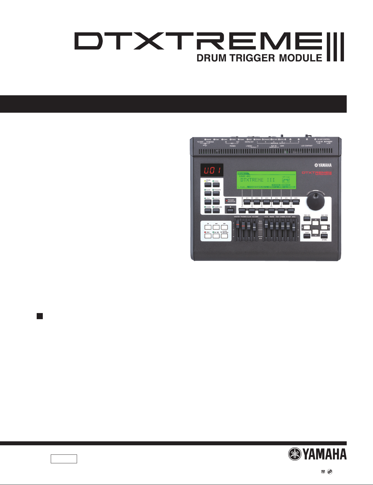
DTXT3
SERVICE MANUAL
SERVICE MANUAL
CONTENTS(目次)
SPECIFICATIONS(総合仕様) ............................... 3/4
PANEL LAYOUT(パネルレイアウト) ....................... 5
CONNECTING THE PADS(パッドの接続) ..............7
CIRCUIT BOARD LAYOUT (ユニットレイアウト)...... 9
DISASSEMBLY PROCEDURE(分解手順) ............. 10
OPTIONAL DIMM INSTALLATION
(DIMM(拡張メモリー)の取り付け) ........................ 16
LSI PIN DESCRIPTION(LSI 端子機能表) .............. 21
IC BLOCK DIAGRAM(IC ブロック図) ................... 25
CIRCUIT BOARDS(シート基板図) ........................ 27
TEST PROGRAM(テストプログラム) .............. 44/63
DEFAULT SETTING(出荷時の設定) ...................... 82
SAVING and LOADING A FILE
(ファイルのセーブ&ロード) ................................... 83
011903
ED
20080401-
オープンプライス
INITIAL FACTORY SETTING
(ファクトリーセット) .............................................. 85
VERSION UPDATE(バージョンアップ) ................ 87
MEMORY STRUCTURE(メモリー構成) ..........88/89
DISPLAY MESSAGES(メッセージリスト) ......90/92
BOOT SEQUENCE(起動シーケンス) ............... 94/95
MIDI IMPLEMENTATION CHART ............................ 96
MIDI DATA FORMAT ................................................ 98
PARTS LIST
BLOCK DIAGRAM(ブロックダイアグラム)
WIRING(結線図)
OVERALL CIRCUIT DIAGRAM(総回路図)
HAMAMATSU, JAPAN
Copyright (c) Yamaha Corporation. All rights reserved. PDF ’08.04
DTXTREME Ⅲ
IMPORTANT NOTICE
This manual has been provided for the use of authorized Yamaha Retailers and their service personnel. It has been assumed that basic
service procedures inherent to the industry, and more specifically Yamaha Products, are already known and understood by the users,
and have therefore not been restated.
WARNING : Failure to follow appropriate service and safety procedures when servicing this product may result in personal injury,
IMPORTANT : This presentation or sale of this manual to any individual or firm does not constitute authorization certification,
The data provided is belived to be accurate and applicable to the unit(s) indicated on the cover. The research engineering, and service
departments of Yamaha are continually striving to improve Yamaha products. Modifications are, therefore, inevitable and changes in
specification are subject to change without notice or obligation to retrofit. Should any discrepancy appear to exist, please contact the
distributor’s Service Division.
WARNING : Static discharges can destroy expensive components. Discharge any static electricity your body may have accumulated
destruction of expensive components and failure of the product to perform as specified. For these reasons, we advise
all Yamaha product owners that all service required should be performed by an authorized Yamaha Retailer or the
appointed service representative.
recognition of any applicable technical capabilities, or establish a principal-agent relationship of any form.
by grounding yourself to the ground bus in the unit (heavy gauge black wires connect to this bus.)
IMPORTANT : Turn the unit OFF during disassembly and parts replacement. Recheck all work before you apply power to the unit.
WARNING: This product contains chemicals known to the State of California to cause cancer, or birth defects or other reproductive harm.
DO NOT PLACE SOLDER, ELECTRICAL/ELECTRONIC OR PLASTIC COMPONENTS IN YOUR MOUTH FOR ANY REASON WHAT SO EVER!
Avoid prolonged, unprotected contact between solder and your skin! When soldering, do not inhale solder fumes or expose eyes to solder/
flux vapor!
If you come in contact with solder or components located inside the enclosure of this product, wash your hands before handling food.
WARNING
Components having special characteristics are marked and must be replaced with parts having specifi cation equal to those
originally installed.
印の部品は、安全を維持するために重要な部品です。交換する場合は、安全のために必ず指定の部品をご使用ください。
SAVING DATA(データの保存)
Saving and backing up your data
• DRAM data is lost when you turn off the power
to the instrument. Save the data to external
Be sure to
• Never attempt to turn off the power while data
perform it
Saving factory preset data
• When you save your original data to flash
Be sure to
perform it
Backing up the external USB storage device
• To protect against data loss through media
Be sure to
perform it
USB storage device.
is being written to Flash ROM (while a “Please
keep power on” message is shown). Turning
the power off in this status results in loss of all
user data and may cause the system to freeze
(due to corruption of data in the Flash ROM).
This means that this instrument may not be
able to start up properly, even when turning the
power on next time.
ROM, the factory preset data in some area of
the fl ash ROM will be lost. Before saving your
original data, be sure to save the factory preset
data to external USB storage device.
damage, we recommend that you save your
important data onto two USB storage devices.
作成したデータの保存とバックアップ
・DRAM のデータは電源を切ると消えてしまい
ます。保存しておきたいデータは外部 USB 記
必ず実行
・フラッシュ ROMへの書き込み中 ( 画面に
憶装置に保存してください。
「Pleasekeep power on.」と表示されます ) に、
絶対に電源を切らないでください。ユーザー
メモリー上のデータが失われたりシステム
データが壊れたりして、次に電源を入れたと
きに正常に起動しなくなる恐れがあります。
工場出荷時のデータの保存
・ご自身で作成したデータをフラッシュ ROM に
保存すると、フラッシュ ROM 上で工場出荷時
必ず実行
のデータが消えてしう領域があります。あら
かじめ工場出荷時のデータを外部 USB 記憶装
置に保存してください。
外部 USB記憶装置のバックアップ
・保存した外部 U SB 記憶装置の万一の事故に備
えて、大切なデータはコンピューターや予備
必ず実行
の USB 記憶装置にバックアップとして保存さ
れることをおすすめします。
2
SPECIFICATIONS
Tone Generator Tone Generator AWM2
Polyphony 64 notes
Wave 205MB (when converted to 16-bit linear format)
Voice Preset: 1,115 drum voices, 211 melody voices (GM)
Drum Kit Preset: 50 kits
Effects Reverb 9 types
Trigger Trigger Setup Preset: 7
Pad songs play, chace, cutoff
Sequencer Note Capacity Approx. 152,000 notes
Note Resolution 480 ppq (parts per quarter note)
Song Recording type Real time
Song tracks 2 tracks
Songs Demo: 3 songs
Sequence Formay DTXTREME III Original Format, SMF format 0
Click Tempo 30 – 300 , Tap tempo
Beat 1/4 – 16/4, 1/8 – 16/8, 1/16 – 16/16
Timing Accent, Quarter note, Eighth note, Sixteenth note, Triplet
Click Voices Preset: 8
Training Functions Measure break, Groove check, Rhythm gate
Sampling Samples 1,016 (for the User Voices)
Sampling Sources Audio input signals via AUX IN/SAMPLING IN, Audio output signals via OUTPUT (Resample)
Sample Data Bits 16bit
Sampling Frequency 44.1kHz, 22.05 kHz, 11.025 kHz, 5.5125 kHz (stereo/mono)
Sampling Memory Optionally installed, expandable to 512 MB (256 MB DIMM x 2 slots)
Sample Length Mono: 32MB
Sampling Time 44.1kHz: 6 min. 20 sec.
Sample Format DTXTREME III Original format, WAV, AIFF
Others Controllers
Displays 240 x 64 dot graphic backlit LCD, 7-segment LED (3-digit)
Connectors • MIDI IN/OUT
Power Consumption 18W
Dimensions, Weight 334(W) x 285(D) x 96(H) mm, 3.6kg
Accessories AC Power Adaptor (Yamaha PA-300B, or an equivalent), Module stand, Module stand fastening
User: 50 kits (in the Flash ROM)
External: 1584 kits (or 99 x 16, in the external USB storage device)
Chorus 18 types
Variation 51 types
Insertion 51 types
Master Effect 9 types
Master EQ 5 bands
User: 5
4 songs (max.) can be played simultaneously.
Practice: 44 songs
Pad song: 40 songs
User: 50 songs
User: 1
* DIMMs are not installed to the instrument when shipped from the factory.
Stereo: 64MB
22.05kHz: 12 min. 40 sec.
11.025kHz: 25 min. 20 sec.
5.5125kHz: 55 min. 40 sec.
*Mono/Stereo
Sliders
MASTER, PHONES, CLICK, ACCOMP., KICK, SNARE, TOM, CYMBAL, HI-HAT, MISC.
Data dial
• USB TO DEVICE/TO HOST
• OUTPUT L/MONO, R (Standard phone jack)
• DIGITAL OUT (EIAJ CP1201, IEC60958, S/P DIF)
• INDIVIDUAL OUTPUT 1 – 6 (Standard phone jack)
• Trigger Input jacks 1 – 9, 12 – 15 (Standard stereo phone jack, L:Trigger Signal, R: Rim Switch)
• Trigger Input jacks 10 and 11 (Standard stereo phone jack, L:Trigger Signal, R: Trigger Signal)
• AUX IN/SAMPLING IN (Standard stereo phone jack)
• PHONES (Standard stereo phone jack)
• HI-HAT CONTROL (Standard stereo phone jack)
• DC IN 16V
screws (4; included)
Owner’s Manual, Data List
DTXTREME Ⅲ
3
DTXTREME Ⅲ
総合仕様
音源部 音源方式 AWM2
最大同時発音数 64音
波形メモリー 205MB相当(16bitリニア換算)
ボイス数 ドラム/パーカッション:1,115音色
ドラムキット数 プリセット:50キット
エフェクター バリエーション(ドラムキット用)x51タイプ、コーラスx19タイプ、リバーブx9タイプ、
トリガー トリガーセットアップ プリセット:7種類
パッドソング スタート/ストップ、チェイス、カットオフ
シーケンサー シーケンサー容量 約152,000音
音符分解能 4分音符/480
レコーディング方式 リアルタイム
トラック数 2
ソング数 デモソング:3曲
シーケンスフォーマット DTXTREMEⅢオリジナルフォーマット
メトロノーム テンポ 30〜300、タップテンポ機能
ビート 1/4〜16/4、1/8〜16/8、1/16〜16/16
タイミング アクセント、4分音符、8分音符、16分音符、3連符
クリックボイス プリセット:8種類
練習機能 メジャーブレイク、グルーブチェック、リズムゲート
サンプラー 最大サンプル数 1,016(ユーザーボイスとして使用)
サンプリングソース アナログ入力L/R、ステレオアウト(リサンプリング)
サンプルデータビット 16bit
サンプリング周波数 44.1kHz、22.05kHz、11.025kHz、5.5125kHz(ステレオ/モノ)
波形メモリー 最大拡張時512MB(256MBDIMMx2)
最大サンプルサイズ 1モノサンプル:32MB
1回あたりのサンプリング時間
サンプルフォーマット DTXTREMEⅢオリジナルフォーマット、WAV、AIFF
その他 操作子 スライダーボリューム(MASTER、PHONES、CLICK、ACCOMP、KICK、SNARE、TOM、
ディスプレイ 240x64ドット グラフィックLCD(バックライト付)、3桁 7セグメントLED
接続端子 トリガー入力1-9、12-15(ステレオ標準フォーン端子L:トリガー、R:リムスイッチ)
消費電力 18W
寸法、重量 334(W)x285(D)x96(H)mm、3.6kg
付属品 電源アダプター(PA-300B)、保証書、取扱説明書、データリスト、
キーボード:211音色
ユーザ:50キット
インサーション(AUXIN/SAMPLINGIN用)x51タイプ、マスターエフェクトx9タイプ、
マスターEQ(5バンド)
ユーザ:5種類
最大同時4曲再生可能
練習曲:44曲
パッドソング:40曲
ユーザ:50曲
SMFフォーマット
ユーザ:1種類
※工場出荷時にはDIMMは装着されていません。
1ステレオサンプル:64MB
44.1kHz:約6分20秒、22.05kHz:約 1 2 分40秒、11.025kHz:約25分20秒、
5.5125kHz:約55分40秒
※ステレオ/モノいずれの場合でも同様
CYMBAL、HI-HAT、MISC)
データダイアル
トリガー入力10/11(ステレオ標準フォーン端子L:トリガー、R:トリガー)
HI-HATCONTROL(ステレオ標準フォーン端子)
OUTPUTL/MONO、R(標準フォーン端子)、DIGITALOUT(S/PDIF)
INDIVIDUALOUTPUT1-6(標準フォーン端子)
PHONES(ステレオ標準フォーン端子)、AUXIN/SAMPLINGIN(ステレオ標準フォーン)
MIDIIN/OUT、USB(TOHOST、TODEVICE)、DCIN
モジュールホルダー、モジュールホルダー止めネジ:4本
4
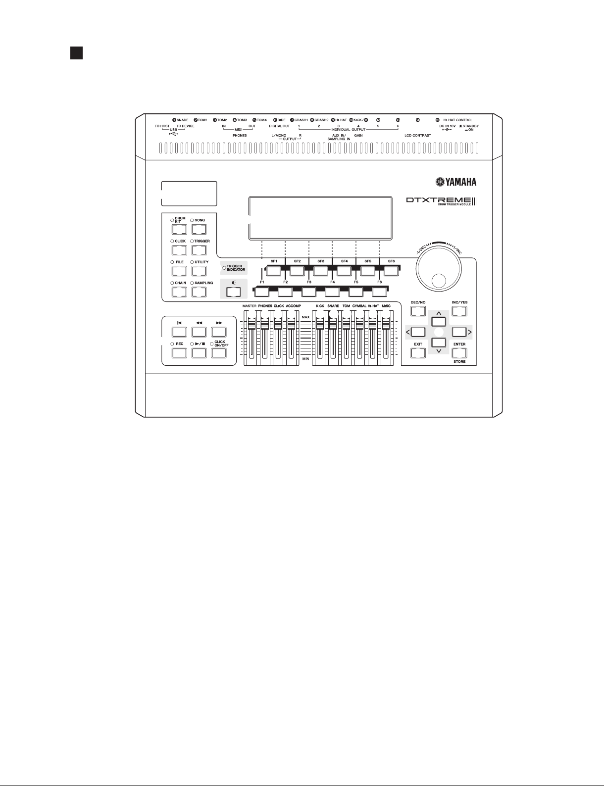
PANEL LAYOUT(パネルレイアウト)
• Front Panel(フロントパネル)
4
DTXTREME Ⅲ
q LCD display
w LED display
e [DRUM KIT] button
r [CLICK] button
t [FILE] button
y [CHAIN] button
u [SONG] button
i[TRIGGER]button
o [UTILITY] button
!0 [SAMPLING] button
!1 TRIGGER INDICATOR
!2 Audition button
!3 [F1] − [F6]
(Function) buttons
!4 [SF1] − [SF6]
(Function) buttons
!5 Transport buttons
[
w
] button
[
1
] button
[
¡
] button
[REC] button
[
3
/ 7 ] button
[CLICK ON/OFF] button
) 2
0 *
1 -
6
!6 [MASTER] slider
!7 [PHONES] slider
!8 [CLICK] slider
!9 [ACCOMP] slider
@0 [KICK] slider
@1 [SNARE] slider
@2 [TOM] slider
@3 [CYMBAL] slider
@4 [HI-HAT] slider
@5 [MISC] slider
@6 Data dial
@7 [DEC/NO] button
@8 [INC/YES] button
@9 Cursor buttons
#0 [EXIT] button
#1 [ENTER/STORE] button
/
qLCD(液晶ディスプレイ)
wLED ディスプレイ
e[DRUMKIT](ドラムキット)
ボタン
r[ C L I C K ] (クリック)ボタン
t[FILE](ファイル)ボタン
y
[ C H AI N ] (チェーン)ボタン
u[SONG](ソング)ボタン
i[TRIGGER](トリガー)
ボタン
o[UTILITY](ユーティリティ)
ボタン
!0
[SAMPLING](
ボタン
!1TRIGGERINDICATOR
(トリガーインジケーター)
!2Audition(
ボタン
!3[F1] 〜 [F6](ファンクショ
ン)ボタン
!4[SF1] 〜 [SF6](サブファ
ンクション)ボタン
!5トランスポートボタン
[
w
](トップ)ボタン
サンプリング
オーディション
)
)
[
1
](巻き戻し)ボタン
[
¡
](早送り)ボタン
[REC](録音)ボタン
[
3
/ 7](再生/停止)ボ タ ン
[CLICKON/OFF]ボタン
!6[MASTER] スライダー
!7[PHONES] スライダー
!8[CLICK] スライダー
!9[ACCOMP] スライダー
@0[KICK]スライダー
@1[SNARE] スライダー
@2[TOM] スライダー
@3[CYMBAL] スライダー
@4[HI-HAT] スライダー
@5[MISC] スライダー
@6データダイアル
@7[DEC/NO](
ボタン
@8
[INC/YES](
ボタン
@9カーソルボタン
#0[EXIT] ボタン
#1[ENTER/STORE] ボタン
デック/ノー
インク / イエス
)
)
5
DTXTREME Ⅲ
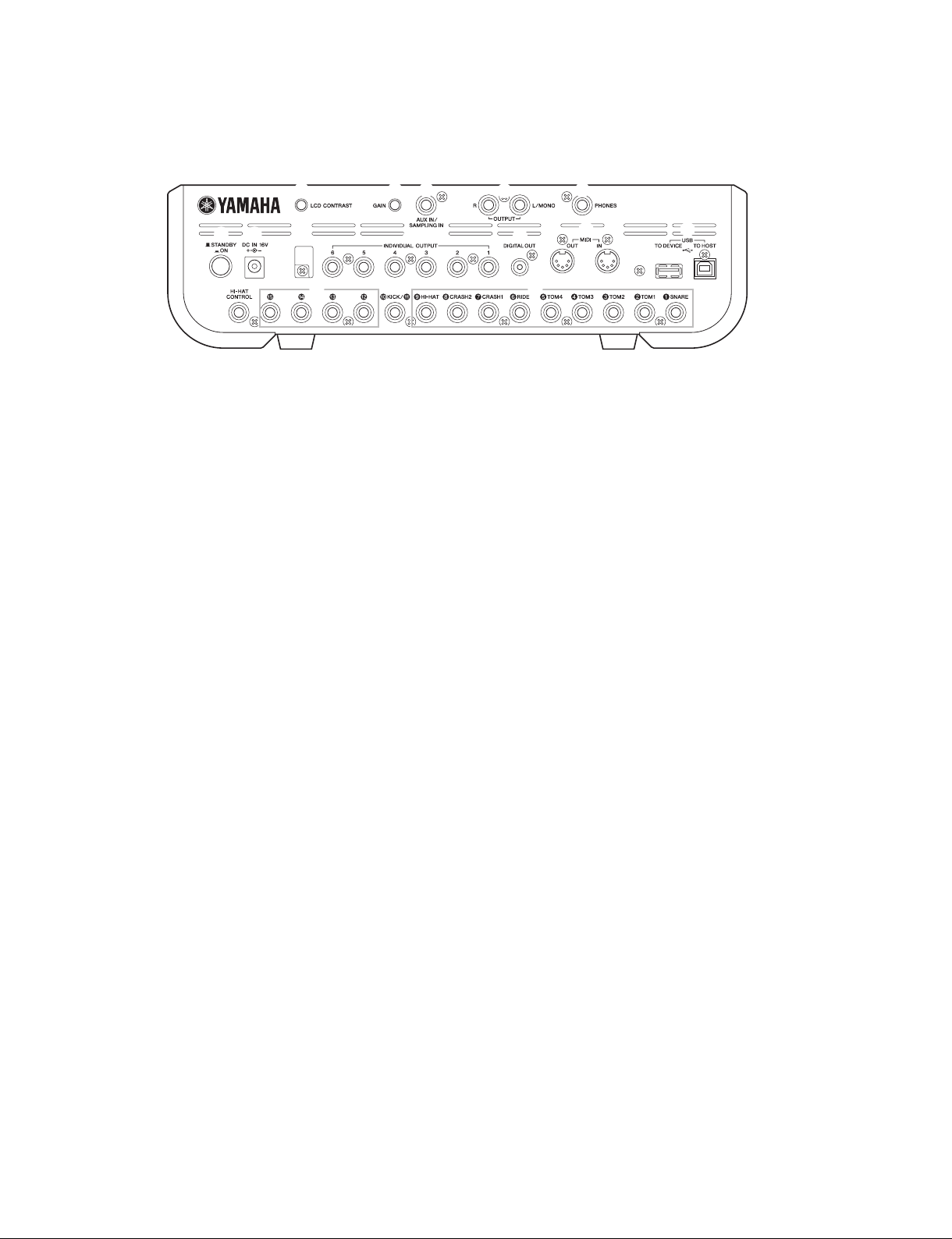
• Rear Panel(リアパネル)
0
4/
)
1
-
q [STANDBY/ON] switch
w [DC IN] terminal
e Cable clip
r [LCD CONTRAST] Control
t [GAIN] knob
y [AUX IN/SAMPLING IN] jack
u [OUTPUT L/MONO] and [OUTPUT R] jacks
i [PHONES] jack
o [INDIVIDUAL OUTPUT 1 − 6] jacks
!0 [DIGITAL OUT] connector
!1 [MIDI IN/OUT] connectors
!2 [USB TO DEVICE] and [USB TO HOST] terminals
!3 [HI-HAT CONTROL] jack
!4 Trigger Input jack ( qSNARE − oHI-HAT)
!5 Trigger Input jack (!0/!1 KICK )
!6 Trigger Input jack (!2 − !5)
6
2
*
q[STANDBY/ON]( スタンバイ / オン ) スイッチ
w [DCIN] 端子
e コードフック
r [LCDCONTRAST](LCD コントラスト ) ノブ
t [GAIN] ノブ
y [AUXIN/SAMPLINGIN] 端子
u [OUTPUTL/MONO]、[OUTPUTR] 端子
i [PHONES]( ヘッドフォン ) 端子
o [INDIVIDUALOUTPUT1〜6] 端子
!0 [DIGITALOUT] 端子
!1 [MIDIIN/OUT] 端子
!2 [USBTODEVICE]、[USBTOHOST] 端子
!3 [HI-HATCONTROL]( ハイハットコントロール ) 端子
!4 トリガー入力端子 (qSNARE〜oHI-HAT )
!5
トリガー入力端子 (!0/!1KICK )
!6 トリガー入力端子 (!2〜!5 )
6
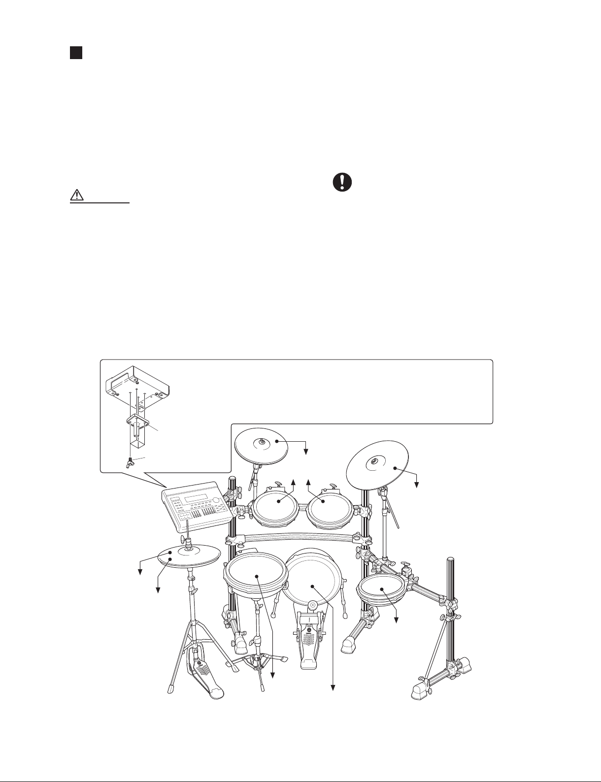
CONNECTING THE PADS(パッドの接続)
DTXTREME Ⅲ
Referring to the illustration below or next page, connect
the output cable from each pad to each Trigger Input jack
located on the rear panel of the DTXTREMEⅢ. All Trigger
Input jacks are conveniently labeled (qSNARE, etc.), so
make sure each pad is connected to its corresponding
Trigger Input jack.
WARNING
To prevent electric shock and damage to the devi-
•
ces, make sure the power is switched OFF on the
DTXTREMEⅢ and all related devices before making any
connections to the DTXTREMEⅢ’s input and output
jacks.
●
DTXTREMEⅢ Standard Set(スタンダードセット)
DTXTREMEⅢ
Holder
(
included
(
Attaching the holder
Attach the included holder to the DTXTREMEⅢ using the wing bolts.
Be sure to use the included screws.
*
DTXTREMEⅢの取り付け
DTXTREMEⅢに付属のモジュールホルダーとちょうボルトを使って、左図のように取り付けます。
必ず付属の止めネジを使用してください。
*
モジュールホルダー
(
付属品
)
))
下の図または次ページの図を参考に、各パッドからの出
力ケーブルを DTXTREME
Ⅲ
リアパネルの各トリガー入
力端子へ接続します。各トリガー入力端子には、それぞ
れ接続するパッドの名称が「q SNARE」などと印刷され
ていますので、該当するパッドを接続します。
・DTXTREMEⅢの入出力端子にケーブルを接続
する際は、感電と機器の損傷を防ぐため、必ず
DTXTREMEⅢおよび各機器の電源を切った状態
で行なってください。
Wing Bolt
x 4 (included
DTXTREMEⅢ
to -HI-HAT
to HI-HAT
CONTROL
(
ちょうボルト
(
付属品
RHH135
)
))
PCY135
TP120SD
to 4TOM1
TP100
to /SNARE
to 2CRASH
to )TOM2
KP125
to KICK
PCY155
TP100
Foot pedal is not included
*
in the Standard Set.
フットペダルはスタンダード
*
セットには含まれません。
/
to 6RIDE
TP100
to 0TOM3
7
DTXTREME Ⅲ
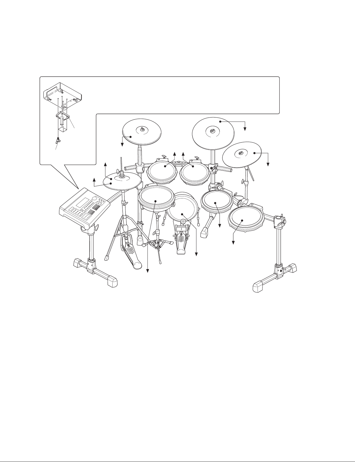
●
DTXTREMEⅢ Special Set(スペシャルセット)
DTXTREMEⅢ
(
(
(
Wing Bolt
ちょうボルト
x 4 (included
DTXTREMEⅢ
Holder
モジュールホルダー
(
included
付属品
)
(
))
付属品
to HI-HAT
CONTROL
)
))
to -HI-HAT
Attaching the holder
Attach the included holder to the DTXTREMEⅢ using the wing bolts.
Be sure to use the included screws.
*
DTXTREMEⅢの取り付け
DTXTREMEⅢに付属のモジュールホルダーと ちょうボルトを使って、左図のように取り付けます。
必ず付属の止めネジを使用してください。
*
to 6RIDE
to 2CRASH1
PCY135
to 4TOM1
to )TOM2
PCY155
PCY135
TP100
TP100
to *CRASH2
RHH135
TP120SD
TP100
KP125
TP100
to 0TOM3
to 1TOM4
to /SNARE
to KICK /
Foot pedal is not included
*
in the Special Set.
フットペダルはスペシャル
*
セットには含まれません。
8
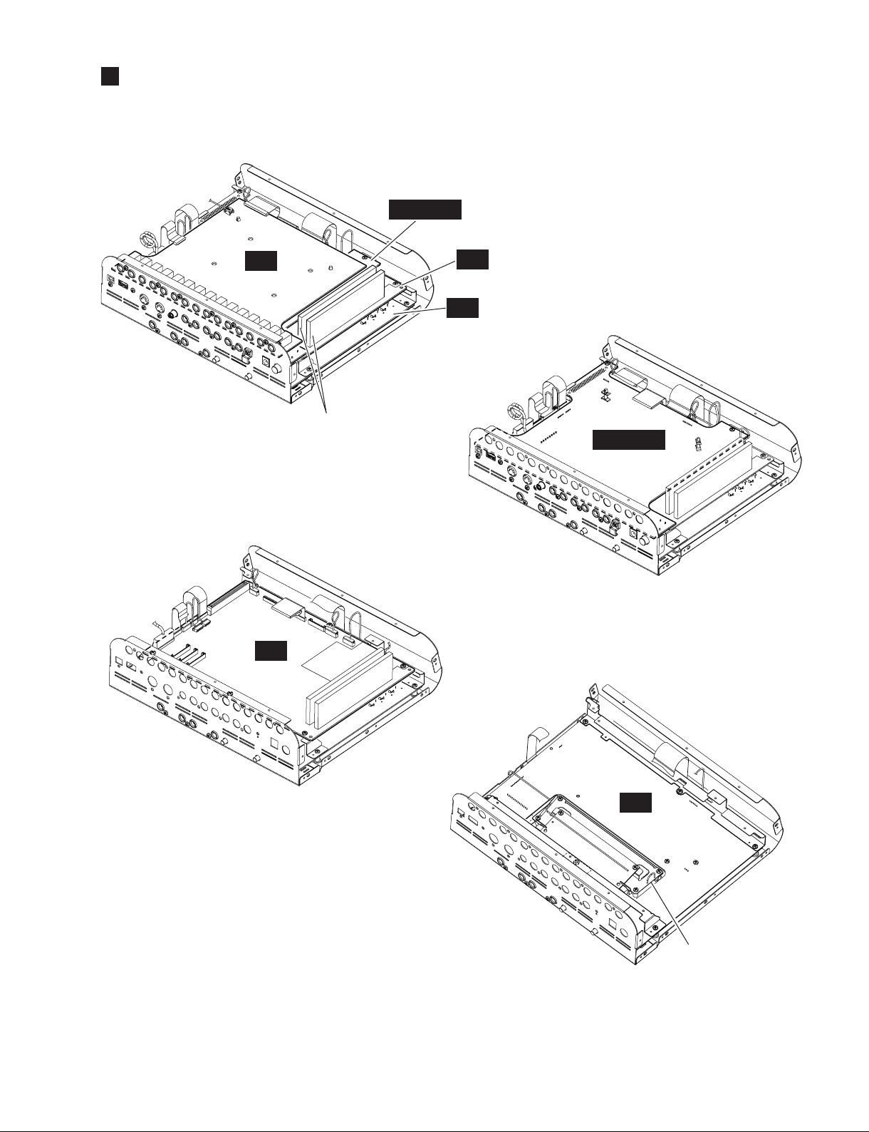
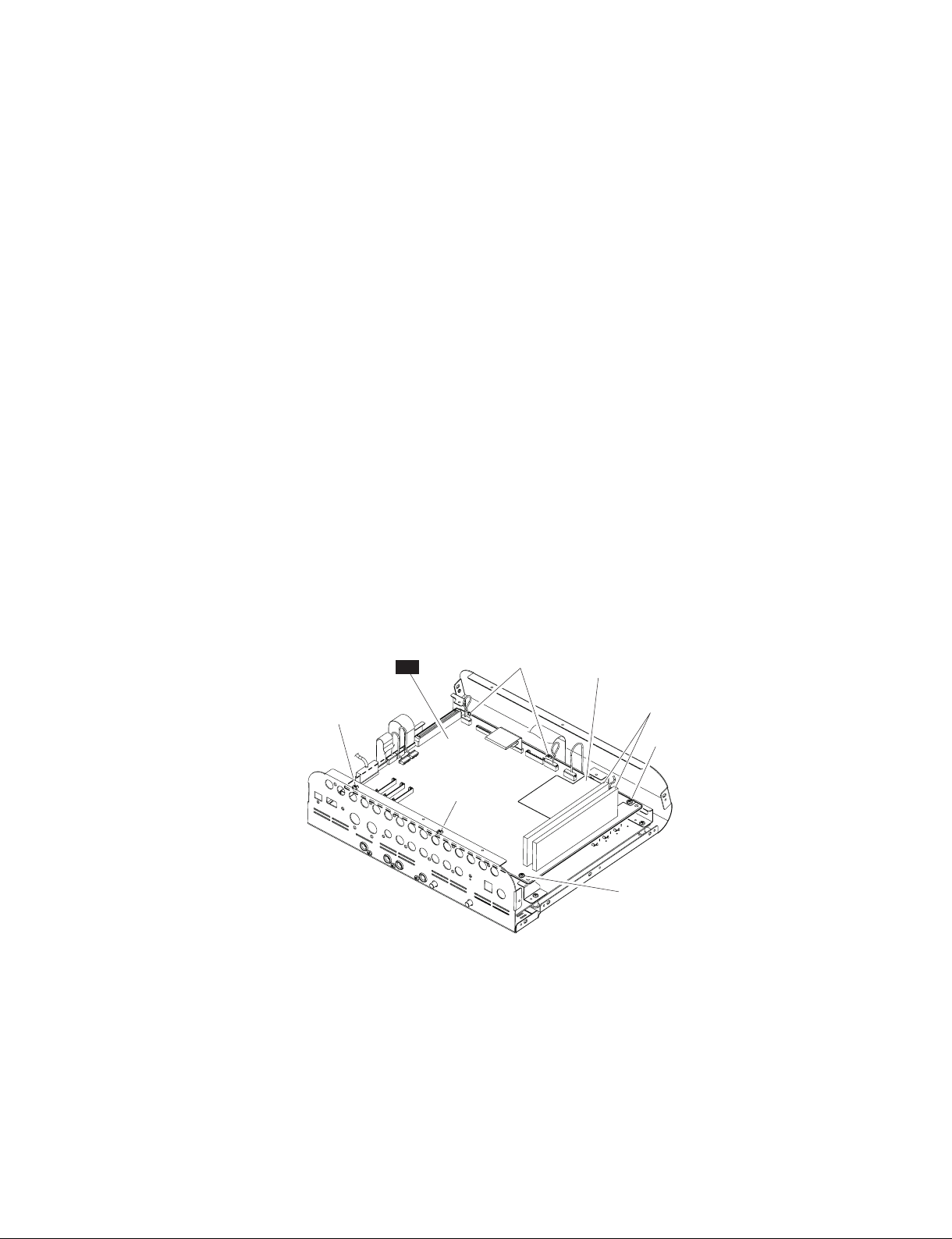
CIRCUIT BOARD LAYOUT(ユニットレイアウト)
<Bottom view>
DMSUB
DTXTREME Ⅲ
<Bottom view>
JK
Optional DIMM
(拡張メモリー)
DM
DM
PN
<Bottom view>
DMSUB
<Bottom view>
PN
Display assembly
(ディスプレイ Assy)
9
DTXTREME Ⅲ
DISASSEMBLY PROCEDURE(分解手順)
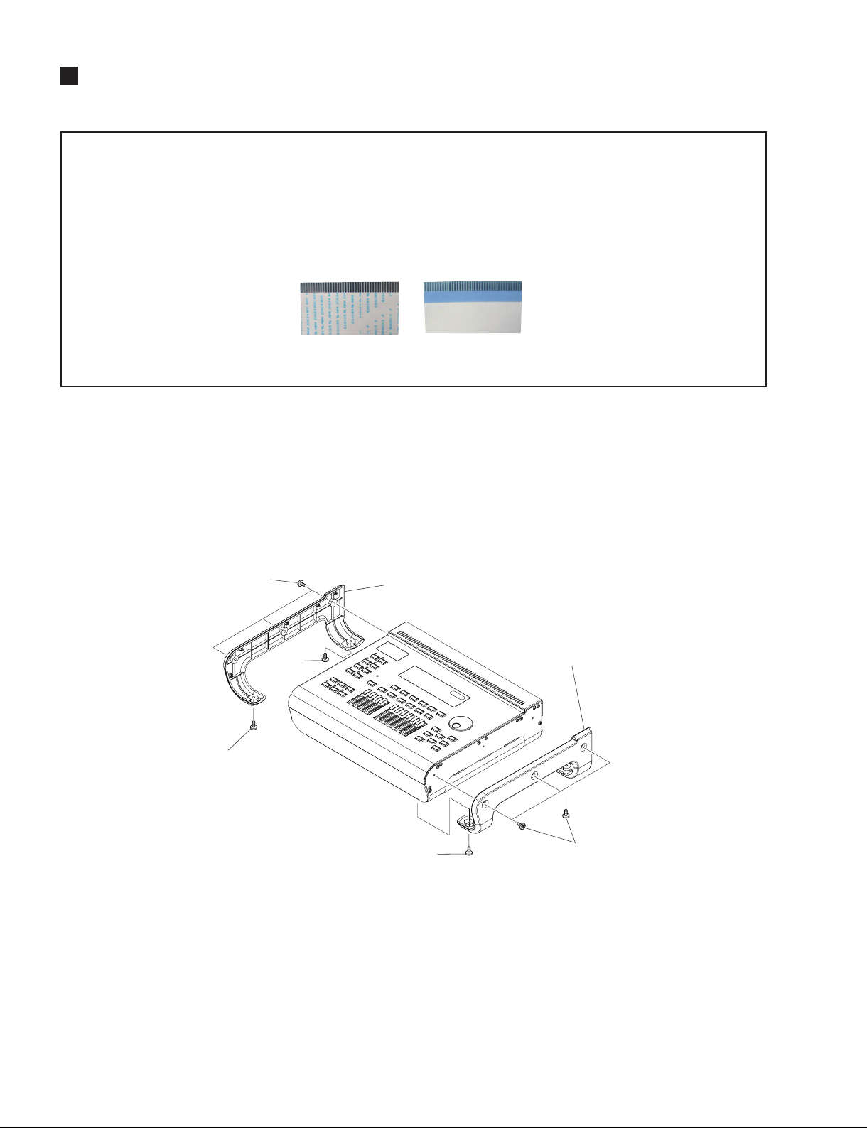
Precautions(注意事項)
•
Notes on Flat Cable
Contacts are visible through the back side. When
connecting to the connector, pay attention not to
insert the cable inversely. (Photo A)
•
During assembly, pay attention that connectors,
cables or the like are not pinched by circuit boards,
frames, etc.
PhotoA( 写真 A)
•
フラットケーブルの注意
接点が裏面から透けて見えます。コネクタにケーブル
の表・裏を逆に差し込まないように注意して取り付け
てください。(写真 A)
•
組み立てるときは、基板やフレームなどでコード類を
はさまないように注意してください。
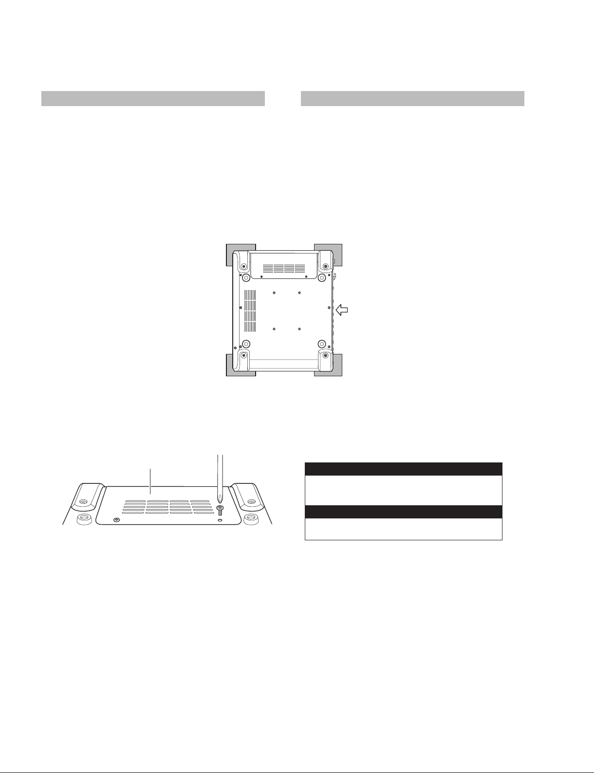
1. Side Cover L & R
(Time required: About 2 minute)
1-1 Remove the following screws and remove the side
cover L and R. (Fig. 1)
[400]: 5pcs. (L) and 5pcs. (R)
[400]
[400]
[400]
1. サイドカバーL、R(所要時間:約 2 分)
1-1 下記のネジを外して、サイドカバー L とサイドカ
[400]: 5 本(左側)、5 本(右側)
Side cover L
(サイドカバーL)
[400]
バー R を外します。(図 1)
Side cover R
(サイドカバーR)
[400]
10
[400]:PWHeadTappingScrew-B(B タイト+ PWH)
3.0X8MFZN2B3(WE975300)
Fig.1( 図 1)
DTXTREME Ⅲ
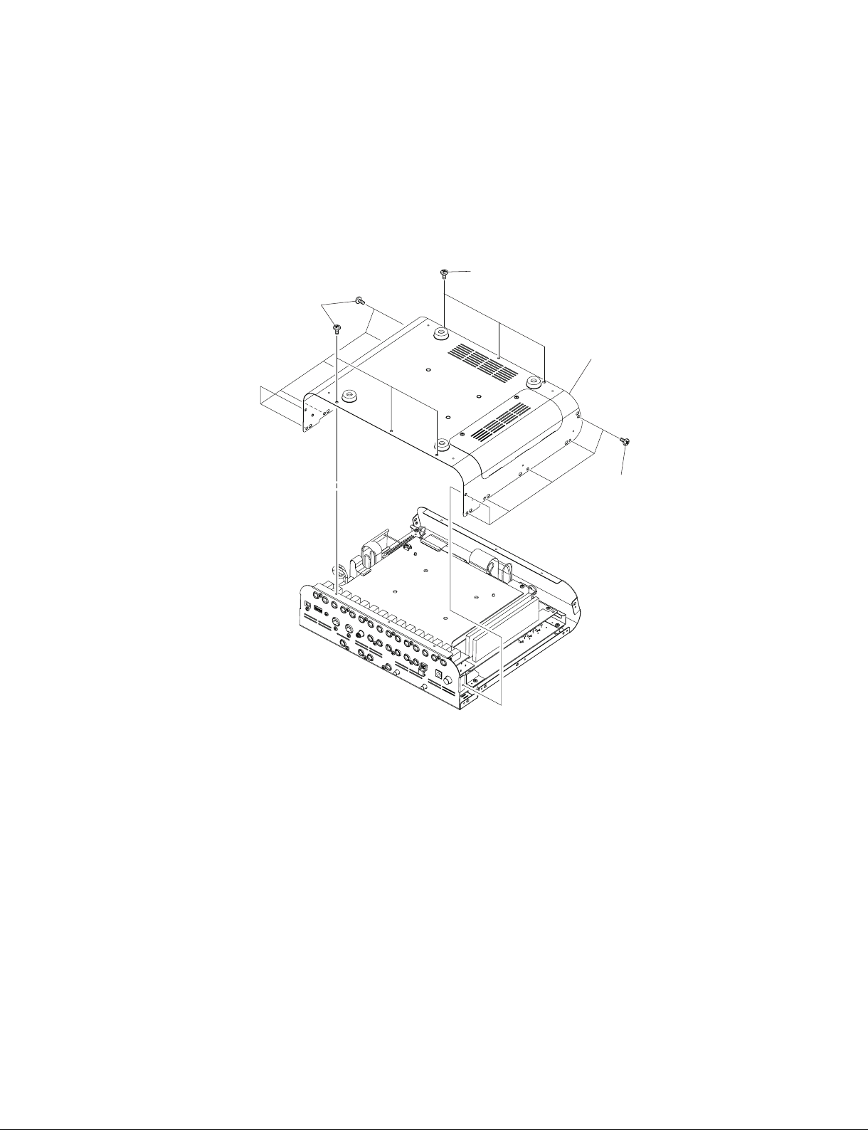
2. Bottom Case
(Time required: About 5 minutes)
2-1 Remove the side cover L and R. (See procedure 1.)
2-2 Remove the following screws and remove the bot-
tom case. (Fig. 2)
[410A]: 18pcs.
<Bottom view(底から見た図)>
[410A]
2. ボトムケース(所要時間:約 5 分)
2-1 サイドカバー L、R を外します。(1 項参照)
2-2 下記のネジを外して、ボトムケースを外します。
(図 2)
[410A]: 18 本
[410A]
Bottom case
(ボトムケース)
[410A]
[410A]:BindHeadTappingScrew-B(B タイト+ BIND)
3.0X8MFZN2W3(WE774300)
Fig.2( 図 2)
11
DTXTREME Ⅲ
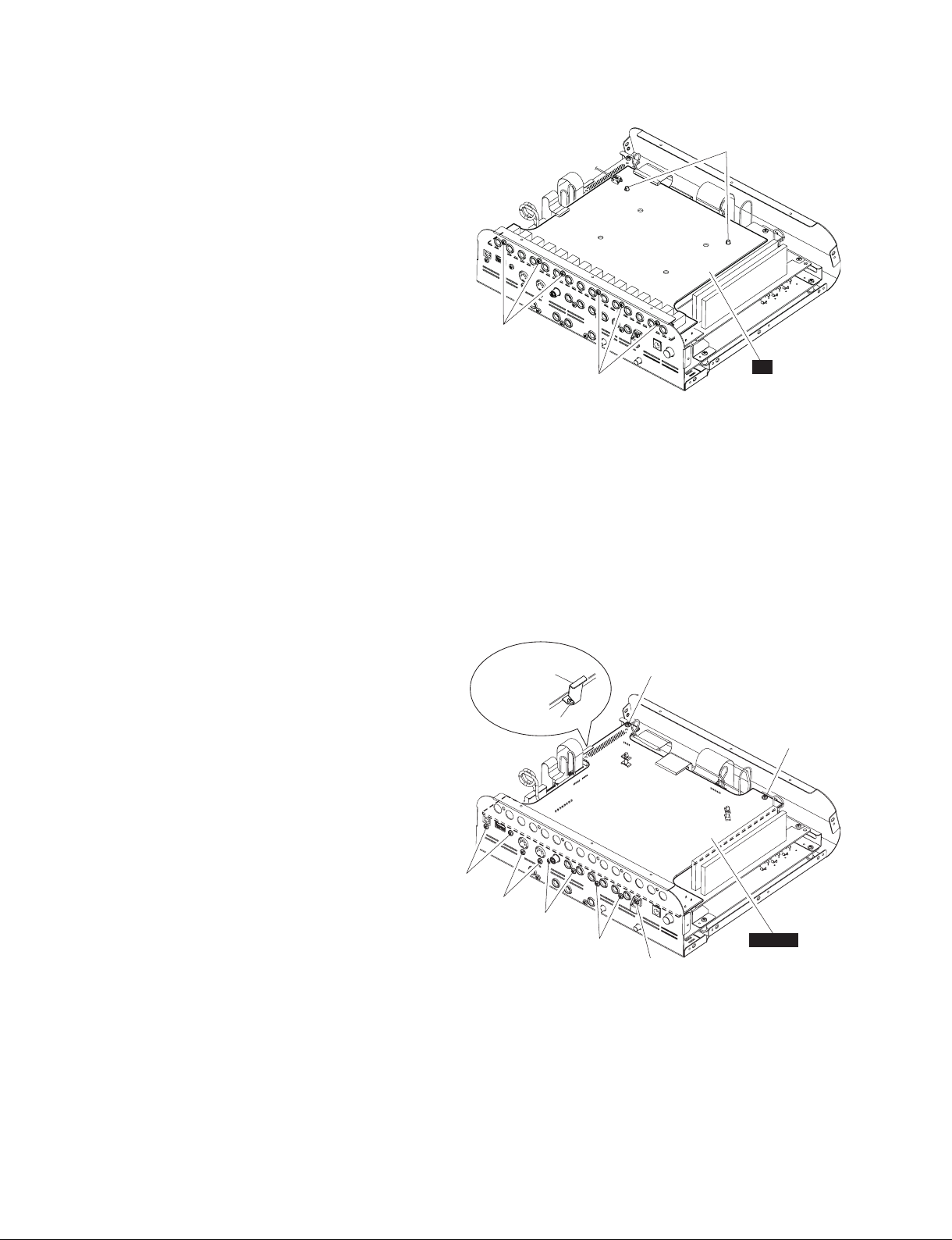
3. JK Circuit Board
(Time required: About 6 minutes)
3-1 Remove the side cover L and R. (See procedure 1.)
3-2 Remove the bottom case. (See procedure 2.)
3-3 Remove the following screws and remove the JK
circuit board from the PCB locking spacer. (Fig. 3)
[390A]: 6pcs.
PCB Locking Spacer
: 2pcs
(Remove the head portion from
the hole of the JK circuit board
while holding the head portion
with pliers or the like.)
3. JK シート(所要時間:約 6 分)
3-1 サイドカバー L、R を外します。(1 項参照)
3-2 ボトムケースを外します。(2 項参照)
3-3 下記のネジを外して、ロッキングスペーサから JK
シートを外します。(図 3)
[390A]: 6 本
ロッキングスペーサ :2 個
(頭の部分をペンチ等でつまみ、
JK 基板の穴から外します。)
<Bottom view(底から見た図)>
PCB locking spacer
(ロッキングスペーサ)
[390A]
JK
[390A]
[390A]:BindHeadTappingScrew-B(B タイト+ BIND)
3.0X10MFZN2B3(WE972200)
Fig.3( 図 3)
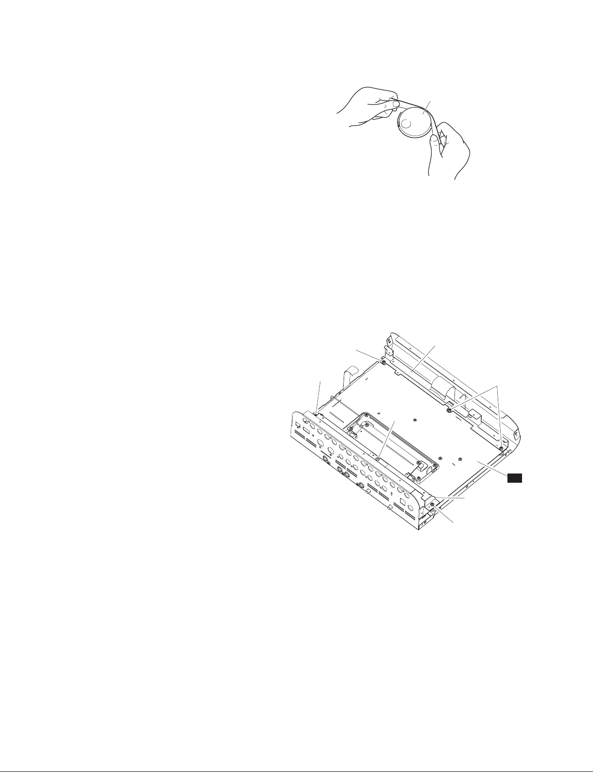
4. DMSUB Circuit Board
(Time required: About 8 minutes)
4-1 Remove the side cover L and R. (See procedure 1.)
4-2 Remove the bottom case. (See procedure 2.)
4-3 Remove the JK circuit board. (See procedure 3.)
4-4 Remove the following screws and remove the sup-
port angle. (Fig. 4)
[410B]: 1pc.
4-5 Remove the following screws and remove the
DMSUB circuit board. (Fig. 4)
[360]: 3pcs.
[380]: 6pcs.
[410C]: 2pcs.
4. DMSUB シート(所要時間:約 8 分)
4-1 サイドカバー L、R を外します。(1 項参照)
4-2 ボトムケースを外します。(2 項参照)
4-3 JK シートを外します。(3 項参照)
4-4 下記のネジを外して、サポートアングルを外しま
す。(図 4)
[410B]: 1 本
4-5 下記のネジを外して、DMSUB シートを外します。
(図 4)
[360]: 3 本
[380]: 6 本
[410C]: 2 本
<Bottom view(底から見た図)>
Support angle
(サポートアングル)
[410B]
[360]
[380]
[380]
[380]
[360]: BondingScrew(小ネジ+ BOND)3.0X6
MFZN2B3(WF303900)
[380]: BondingTappingScrew-B(B タイト+ BOND)
3.0X10MFZN2B3(WE878000)
[410B],[410C]:BindHeadTappingScrew-B(B タイト+ BIND)
3.0X8MFZN2W3(WE774300)
[410C]
DMSUB
[360]
Fig.4( 図 4)
[410C]
12
DTXTREME Ⅲ
5. DM Circuit Board
(Time required: About 9 minutes)
5-1 Remove the side cover L and R. (See procedure 1.)
5-2 Remove the bottom case. (See procedure 2.)
5-3 Remove the JK circuit board. (See procedure 3.)
5-4 Remove the DMSUB circuit board.
(See procedure 4.)
5-5 Remove the following screws and remove the DM
circuit board. (Fig. 5)
[410D]: 6pcs.
The optional DIMM is not part of the DM circuit
*
board. When replacing the DM circuit board, remove the optional DIMM, and install it to a new
DM circuit board. (Fig. 5)
When replacing the DM circuit board, save the
*
whole internal setup data on a USB memory.
(See page 83)
When the connector assembly is disconnected
*
from the connector CN18, the protection sheet
will be disconnected as well. Take care not to
lose the protection sheet.
5. DM シート(所要時間:約 9 分)
5-1 サイドカバー L、R を外します。(1 項参照)
5-2 ボトムケースを外します。(2 項参照)
5-3 JK シートを外します。(3 項参照)
5-4 DMSUB シートを外します。(4 項参照)
5-5 下記のネジを外して、DM シートを外します。(図 5)
[410D]: 6 本
※ 拡張メモリー(オプション)は DM シートの構成
部品ではありません。DM シートを交換する際は、
拡張メモリーを取り外して、新しい DM シートに
取り付けてください。(図 5)
※ DM シートを交換する際は、内部の全ての設定デー
タを USB メモリーにセーブ(保存)してください。
(83 ページ参照)
※ コネクタ CN18 から線材を外した時、保護シート
も外れますので、紛失しないよう注意しててくだ
さい。
<Bottom view(底から見た図)>
DM
[410D]
[410D]
[410D]:BindHeadTappingScrew-B(B タイト+ BIND)
3.0X8MFZN2W3(WE774300)
[410D]
Protection sheet
(保護シート)
Fig.5( 図 5)
Optional DIMM
(拡張メモリー)
[410D]
[410D]
13
DTXTREME Ⅲ
6. PN Circuit Board
(Time required: About 12 minutes)
6-1 Pull out the encoder knob from the control panel
side. (Fig. 6)
6-2 Remove the side cover L and R. (See procedure 1.)
6-3 Remove the bottom case. (See procedure 2.)
6-4 Remove the JK circuit board. (See procedure 3.)
6-5 Remove the DMSUB circuit board.
(See procedure 4.)
6-6 Remove the DM circuit board. (See procedure 5.)
6-7 Remove the following screws and remove the PN
angle R. (Fig. 7)
[410E]: 3pcs.
6-8 Remove the following screws and remove the PN
angle F. (Fig. 7)
[410F]: 3pcs.
6-9 Remove the following screws and remove the PN
circuit board. (Fig. 8)
[390C]: 3pcs.
[410G]: 5pcs.
6. PN シート(所要時間:約 12 分)
6-1 コントロールパネル面よりエンコーダツマミ (S)
を抜いておきます。(図 6)
6-2 サイドカバー L、R を外します。(1 項参照)
6-3 ボトムケースを外します。(2 項参照)
6-4 JK シートを外します。(3 項参照)
6-5 DMSUB シートを外します。(4 項参照)
6-6 DM シートを外します。(5 項参照)
6-7 下記のネジを外して、PN アングル R を外します。
(図 7)
[410E]: 3 本
6-8 下記のネジを外して、PN アングル F を外します。
(図 7)
[410F]: 3 本
6-9 下記のネジを外して、PN シートを外します。(図 8)
[390C]: 3 本
[410G]: 5 本
Encoder knob
(エンコーダーツマミ)
Fig.6( 図 6)
<Bottom view(底から見た図)>
[410F]
[410E]
[410E]
[410E],[410F]: BindHeadTappingScrew-B(B タイト+ BIND)
3.0X8MFZN2W3(WE774300)
PN angle F
(PNアングルF)
[410F]
PN
PN angle R
(PNアングルR)
[410E]
14
Fig.7( 図 7)
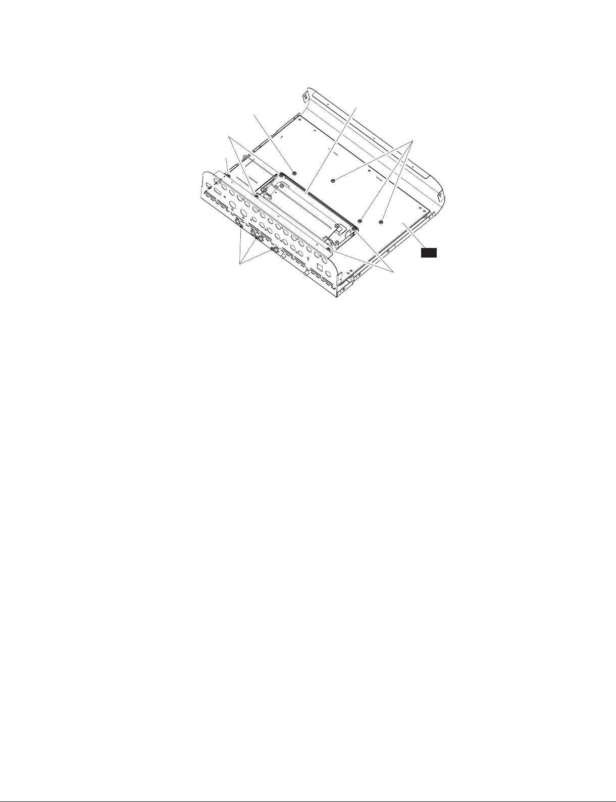
<Bottom view(底から見た図)>
[410G]
DTXTREME Ⅲ
Display assembly
(ディスプレイAss’y)
[410G]
[390C]:
[410G],[410H]:
[410H]
[390C]
BindHeadTappingScrew-B(B タイト+ BIND)
BindHeadTappingScrew-B(B タイト+ BIND)
Fig.8( 図 8)
[410G]
PN
[410H]
3.0X10MFZN2B3(WE972200)
3.0X8MFZN2W3(WE774300)
7. Display Assembly
(Time required: About 11 minutes)
7-1 Remove the side cover L and R. (See procedure 1.)
7-2 Remove the bottom case. (See procedure 2.)
7-3 Remove the JK circuit board. (See procedure 3.)
7-4 Remove the DMSUB circuit board.
(See procedure 4.)
7-5 Remove the DM circuit board. (See procedure 5.)
7-6 Remove the PN circuit board. (See procedure 6.)
7-7 Remove the following screws and remove the dis-
play assembly. (Fig. 8)
[410H]: 4pcs.
7. ディスプレイ Ass'y(所要時間:約 11 分)
7-1 サイドカバー L、R を外します。(1 項参照)
7-2 ボトムケースを外します。(2 項参照)
7-3 JK シートを外します。(3 項参照)
7-4 DMSUB シートを外します。(4 項参照)
7-5 DM シートを外します。(5 項参照)
7-6 PN シートを外します。(6 項参照)
7-7 下記のネジを外して、ディスプレイ Assyを外し
ます。(図 8)
[410H]: 4 本
15
DTXTREME Ⅲ
OPTIONAL DIMM INSTALLATION(DIMM(拡張メモリー)の取り付け)
This section explains how to install DIMM memory modules to the DTXTREMEⅢ .
(ここでは、市販のメモリー(「DIMM」と呼ばれるメモリーモジュール)を取り付ける方法を説明します。)
Installation Precautions
WARNING
• Before beginning installation, switch off the power to the
instrument and connected peripherals, and unplug them
from the power outlet. Installation or removal of any devices should be started ONLY after the instrument (and the
optional hardware) returns to normal room temperature.
Then remove all cables connecting the instrument to other
devices. (Leaving the power cord connected while working
can result in electric shock. Leaving other cables connected
can interfere with work.)
• Be careful not to drop any screws inside the instrument
during installation. (This can be prevented by keeping the
optional units and cover away from the instrument while attaching). If this does happen, be sure to remove the screw(s)
from inside the unit before turning the power on. Loose
screws inside the instrument can cause improper operation
or serious damage.
• Install the optional units carefully as described in the pro-
cedure below. Improper installation can cause shorts which
may result in irreparable damage and pose a fi re hazard.
• Do not disassemble, modify, or apply excessive force to
board areas and connectors on optional units. Bending or
tampering with boards and connectors may lead to electric
shock, fi re, or equipment failures.
CAUTION
• It is recommended that you wear gloves to protect your
hands frommetallic projections on optional units and other
components. Touchingleads or connectors with bare hands
may cause fi nger cuts, and mayalso result in poor electrical
contact or electrostatic damage.
• Be careful of static electricity. Static electricity discharge can
damage the IC chips on the DIMM. Before you handle the
optional DIMM, to reduce the possibility of static electricity,
touch unpainted metal parts or a ground wire on the devices
that are grounded.
Handle the optical units with care. Dropping or subjecting
•
them to any kind of shock may cause damage or result in a
malfunction.
• Do not touch the exposed metal parts in the circuit board.
Touching these parts may result in a faulty contact.
•
Be careful not to misplace any of the screws.
Do not use any screws other than what are installed on the
•
instrument. Use of incorrect screws can cause damage.
拡張部品取り付けに関する注意
・ 取り付け / 取り外し作業は、必ず本体および周辺機器の
電源を切り、本体および取り付けられた拡張部品が十分
に冷めた状態で行なってください。そして、本体の電源
コードのプラグをコンセントから抜き取り、さらに、本
体と周辺機器を接続しているケーブルを抜き取ってから
行なってください。
・ネジ類を本体内部に落とさないように注意してくださ
い。これを防ぐため、拡張部品を取り付けている間、外
したネジやカバーを本体から離れた場所に置いておくよ
うにしてください。落としたネジを内部に放置したまま
電源を入れると、正常に動作しなくなったり、故障した
りする場合があります。
・ 取り付けは、手順に従って注意深く作業してください。
手順に従わなかった場合、製品の破損や故障の原因にな
ることがあります。
・拡張部品のボード部分やコネクターを分解 / 改造したり、
過度な力を加えたりしないでください。ボード部分やコ
ネクター部を曲げたり変形させたりすると、感電や火災、
または故障などの原因になります。
・本体や拡張部品の金具で手を切らないように、厚手の手
袋を着用して作業することをおすすめします。
・ 静電気の発生に注意してください。基板上の ICチップ
などに影響を及ぼす場合があります。基板を持ち上げる
場合など十分に注意の上、あらかじめ塗装面以外の金属
部分に触れておいたり、アースされている機器のアース
線に触れたりなどして、静電気を逃がすようにしてくだ
さい。
・ボードの取り扱いには十分注意してください。落とした
り、衝撃を与えると製品の破損や故障の原因になること
があります。
・基板上の金属部分が露出している部分には、触れないよ
うにしてください。接触不良などの原因になることがあ
ります。
・本体のネジはすべて使用します。なくさないように注意
してください。
・ネジはオプションボードの付属品、または本体に取り付
けられているもの以外は使用しないでください。サイズ
の違うネジを使用すると、製品の破損や故障の原因にな
ることがあります。
16
DTXTREME Ⅲ
Compatible DIMMs
The DTXTREME Ⅲ does not necessarily support all commer-
cially available DIMMs. Yamaha cannot guarantee operation of
DIMMs that you purchase.
Before purchasing DIMMs, please visit the following website:
http://www.yamaha.co.jp/english/product/drums/ed/
DIMM Typed and DIMM Confi guration
• Yamaha recommends that you purchase DIMMs that conform
to the JEDEC* standard. Please be aware, however, that conformance to this standard does not constitute a guarantee that
the DIMMs will operate correctly on the DTXTREME Ⅲ.
*
JEDEC (Joint Electron Device Engineering Council) sets
standards for terminal configurations within electronic
devices.
• Use only 168-pin DIMMs of 64, 128 or 256 MB capacity
(synchronized DRAM; PC100 or PC133).
• When installing DIMMs, make sure to install them in a
matched pair of the same capacity. You cannot install only
one module and leave the second memory socket open. Also
make sure each DIMM in the pair is of the same manufacturer and the same type. DIMMs of different makers and
confi gurations may not work together.
• When purchasing DIMMs, make sure that the DIMM design
does not utilize more than 18 memory chips per module.
(DIMMs comprised of more than 18 chips do not operate
correctly on the DTXTREME Ⅲ.)
DIMM 購入時の注意
市販の DIMM の中には、DTXTREMEⅢで使用できない
ものがあります。動作確認済品番については、インター
ネット下記 URL で確認してください。
http://www.yamaha.co.jp/product/drum/ed
DIMM の種類 / 内部構成に関する注意
・ DIMM は、JEDEC* 仕様準拠のものを推奨しますが、
JEDEC 仕様でも内部回路構成上、コンピューターでは
動作しても、本機では動作しない場合があります。
*
JEDEC(JointElectronDeviceEngineeringCouncil) とは、電
子デバイス技術協議会のことです。電子デバイスの標準的
な端子配列などを規定しています。
・ DIMM は、64MB、128MB、256MB の 168 ピンタイプ、
シンクロナス DRAM 搭載 (100MHz/133MHz) のもの
を使ってください。
・ DIMM は、必ず同じ容量の DIMM を 2 枚 1 組で取り
付けます。1 枚だけの増設はできません。( メモリー
DIMM スロットは 2 つあります。) また、メーカーの
違うもの、メーカーが同じでも品番が違うものを一緒
に取り付けないようにしてください。
・ メモリーチップが 19 個以上載っている DIMM(1 枚に
つき)は、本機では正常に動作しない場合があります。
メモリーチップが 18 個以下の DIMM を使用してくだ
さい。
64MB x 2 = 128MB 128MB x 2 = 256MB
256MB x 2 = 512MB
17
DTXTREME Ⅲ
DIMM Installation
1 Turn the DTXTREME Ⅲ power off, and disconnect
the power cord.
2 Turn over the DTXTREMEⅢ so you canhave direct
access to the underside.
To protect the data dial and sliders from damage, place the DTXTREMEⅢ so the four corners are supported by something that
provides suffi cient support, such as magazines or cushions. Place
supports at all four corners, taking care not to touch the Data dial
and Sliders.
Bottom surface of the
(DTXTREMEⅢ底面)
DTXTREME
DIMM の取り付け手順
1DTXTREMEⅢ本体の電源を切り、電源アダプターコー
ドを抜きます。
2本体を裏返し、底面が見えるように下図の向きに置き
ます。
このとき、データダイアルやスライダーを破損しないように
本体の四隅に雑誌などをクッションにしてその上に乗せます。
Ⅲ
Rear panel
(リアパネル面)
3 Remove the slot cover.
Remove the screws from the slot cover by using a Phillips screw-
driver.
Slot cover
(スロットカバー)
Underside of the DTXTREMEⅢ
(DTXTREMEⅢ底面)
3
底面のスロットカバーを外します。
底面のスロットカバー止めネジ 2 本をドライバーで外し、
本体よりスロットカバーを外します。
IMPORTANT
Keep the removed screws in a safe place. They will
be used when re-attaching the cover to the instrument
after installing the DIMMs.
重要
外したネジはなくさないようにしてください。このネジは、
DIMM取り付け後、再度使用します。
18

DTXTREME Ⅲ
4 Insert the two DIMMs into the DIMM sockets.
●
Location for DIMM installation(DIMMの取り付け位置)
Installing the DIMM modules to the sockets
Make sure that the DIMM module is aligned correctly before you install it.
(DIMMの向きを確かめて取り付けてください。)
Ejector lever
(ロックレバー)
4
DIMM を 2 枚、DIMM スロットに垂直に奥まで差し
込みます。
DIMM slot × 2
(DIMMスロット×2)
DIMM スロットへの取り付け
Notch for alignment
(切り欠き)
4-1 Press the ejector levers to the outside of the socket.
4-2 Insert the DIMM vertically in the socket.
Press the DIMM in fi rmly until it “snaps” or locks in
place.
Confirm whether or not both the levers are firmly
locked.
4-1左右のロックレバーを横に押して、倒します。
4-2DIMM を垂直に、奥まで差し込みます。
同時にレバーが立ち上げられ、DIMM を固定した状態で
ロックされます。
ここで左右のレバーがしっかりロックされているか確認
してください。
19
DTXTREME Ⅲ
5 Re-install the cover you removed in step 3, in re-
verse order.
*When you re-install the cover, make sure to steady the
cover from the side with your hand.
6 Check that the installed DIMMs are functioning
properly.
Set the DTXTREME Ⅲ right-side up, and connect the AC power
adaptor to the DC IN jack of the DTXTREMEⅢ and an AC wall
outlet.
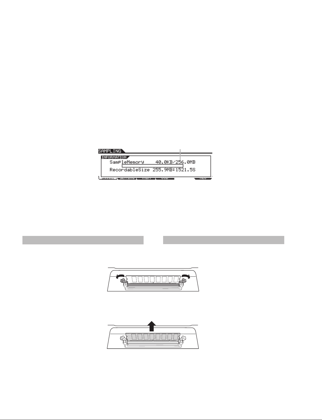
Turn on the power, go to the Sampling mode by pressing the
[SAMPLING] button, then press the [SF6] INF button.
If the DIMMs have been installed properly, the appropriate avail-
able memory size is indicated in the display.
*If the DIMMs have not been installed properly, the Sampling
function will not work correctly. If this occurs, turn the power
off, perform the instructions above again, and make sure to
install the DIMMs fi rmly.
5
手順 3 で取り外したスロットカバーを、逆の手順で取
り付けます。
※スロットカバーを取り付けるときは、横からカバーを本体
側に押さえて取り付けるようにしてください。
6
取り付けた DIMM が正常に機能しているか、確認し
ます。
本体の電源を入れ、[SAMPLING] ボタンを押してサンプリ
ングモードに入ります。[F1]SELECT ボタンを押して、セ
レクト画面を表示させてから [SF6]INFO ボタンを押し、サ
ンプル用のメモリー容量が正しい値になっているか、確認し
てください。
Memory size
(メモリー容量)
※ DIMM が適切に取り付けられていない場合、サンプリン
グ機能が正常に動作しません。このような場合は、電源を
切り、もう一度上記手順に従って、DIMM を確実に取り付
けてください。
Removing DIMMs
1 Press the ejector lever until the DIMM unlocks.
2 Pull the DIMM vertically out of the socket.
DIMM の取り外し方
1左右のレバーを横に押して、ロックを外します。
2DIMM を垂直に引き抜きます。
20
DTXTREME Ⅲ
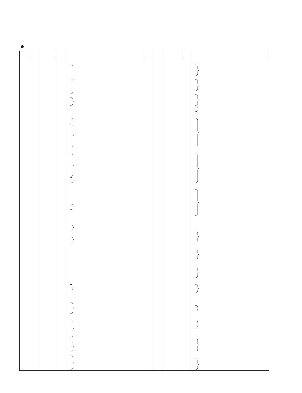
LSI PIN DESCRIPTION(LSI 端子機能表)
AK4393VF-E2 (XW029A00) DAC (Digital to Analog Converter) .........................................................25
AK5381VT-E2 (X5219A00) ADC (Analog to Digital Converter) ...........................................................21
HD6417727F160CV (X2890B00) CPU ...............................................................................................24
T6TZ2XBG-0002 (X7376B00) SWP51 (Tone Generator) ..............................................................22-23
µPD780031AYGK-N09 (XZ916300) E-PNS2a LED/SWITCH DRIVER...............................................21
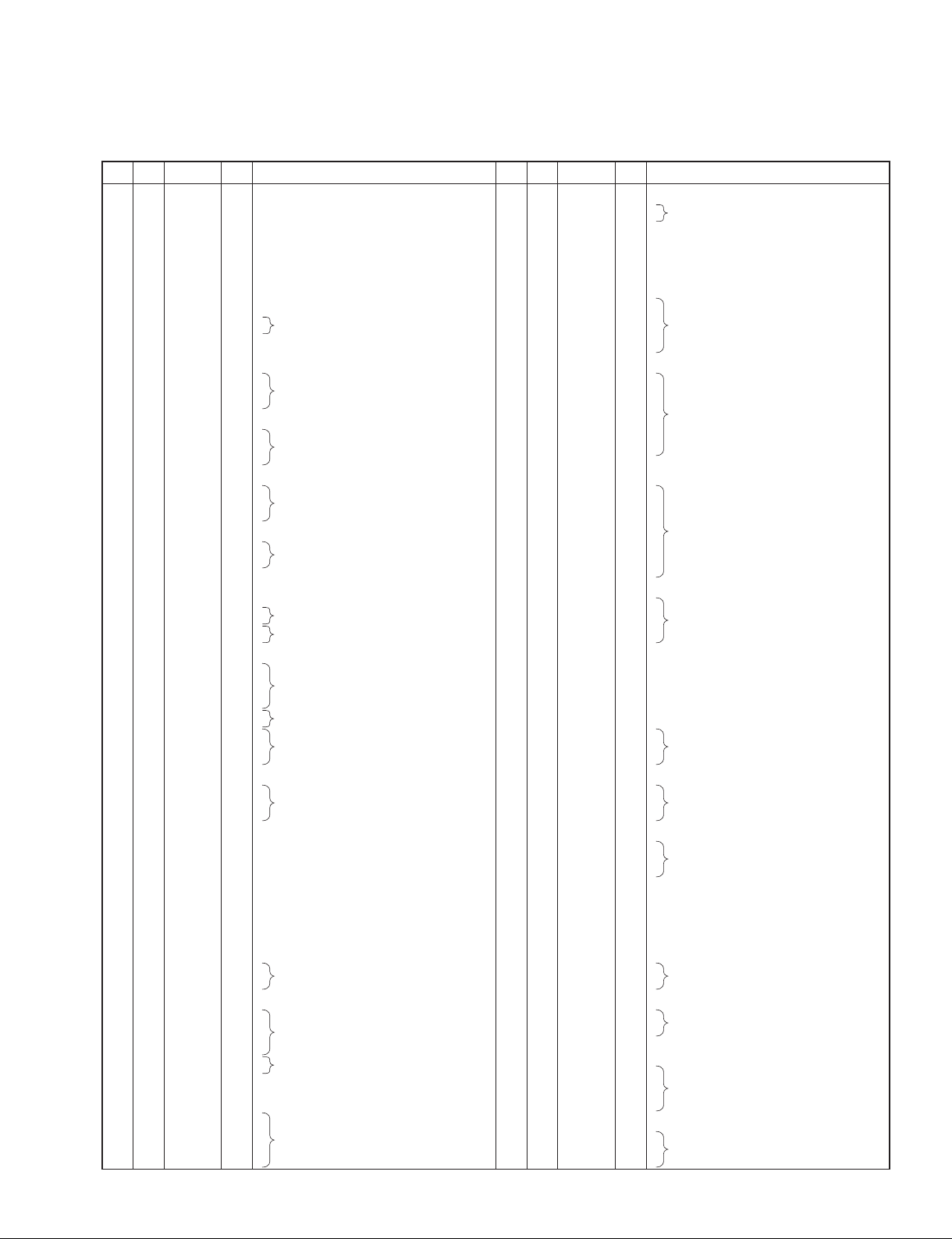
μPD780031AYGK-N09 (XZ916300) E-PNS2a LED/SWITCH DRIVER
PIN
NO.
1
2
3
4
5
6
7
8
9
10
11
12
13
14
15
16
17
18
19
20
21
22
23
24
25
26
27
28
29
30
31
32
P50/A8
P51/A9
P51/A10
P53/A11
P54/A12
P55/A13
P56/A14
P57/A15
Vss0
VDD0
P30
P31
P32/SDA0
P33/SCL0
P34
P35
P36
P20/SI30
P21/SO30
P22/SCK30
P23/RxD0
P24/TxD0
P25/ASCK0
VDD1
AVss
P17/ANI7
P16/ANI6
P15/ANI5
P14/ANI4
P13/ANI3
P12/ANI2
P11/ANI1
I/O FUNCTIONNAME
I/O
I/O
I/O
I/O
I/O
I/O
I/O
I/O
I/O
I/O
I/O
I/O
I/O
I/O
I/O
I/O
I/O
I/O
I/O
I/O
I/O
Port 5 / Higher address bus
-
-
-
I
I
I
I
I
I
I
Ground
Power supply +5 V
Port 3
Port 3 / Serial data input/output
Port 3 / Serial clock input/output
Port 3
Port 2 / Serial data input
Port 2 / Serial data output
Port 2 / Serial clock input/output
Port 2 / Serial data input
Port 2 / Serial data output
Port 2 / Serial clock input/output
Power supply +5 V
Ground
Port 1 / A/D converter analog input
PIN
NO.
33
P10/ANI0
34
AVREF
35
AVDD
36
RESET
37
XT2
38
XT1
39
40
41
42
Vss1
43
P00/INTP0
44
P01/INTP1
45
P02/INTP2
46
P03/INTP3/ADTRG
47
P70/TI00/TO0
48
P71/TI01
49
P72/TI50/TO50
50
P73/TI51/TO51
51
P74/PCL
52
P75/BUZ
53
P64/RD
54
P65/WR
55
P66/WAIT
56
P67/ASTB
57
P40/AD0
58
P41/AD1
59
P42/AD2
60
P43/AD3
61
P44/AD4
62
P45/AD5
63
P46/AD6
64
A47/AD7
IC
X2
X1
I/O FUNCTIONNAME
I/O
I/O
I/O
I/O
I/O
I/O
I/O
I/O
I/O
I/O
I/O
I/O
I/O
I/O
I/O
I/O
I/O
I/O
I/O
I/O
I/O
I/O
I
I
I
I
-
I
-
Port 1 / A/D converter analog input
A/D converter reference voltage input
Analog power supply +5 V
System reset input
Subsystem clock oscillation
Internally connected
Main system clock oscillation
Ground
Port 0 / External interrupt request input
Port 0 / External interrupt request input / Trigger signai input
Port 7 / External count clock input / 16-bit timer/event counter 0 output
Port 7 / Capture trigger input
Port 7 / External count clock input / 8-bit timer/event counter 50 output
Port 7 / External count clock input / 8-bit timer/event counter 51 output
Port 7 / Clock output
Port 7 / Buzzer output
Port 6 / Strobe signal output for reading
Port 6 / Strobe signal output for writing
Port 6 / Wait insertion
Port 6 / Strobe output
Port 4 / Lower address/data bus
PN: IC702
AK5381VT-E2 (X5219A00) ADC (Analog to Digital Converter)
PIN
NO.
1
2
3
4
5
6
7
8
NAME I/O
AINR
AINL
CKS1
VCOM
AGND
VA
VD
DGND
FUNCTION
I
I
I
O
-
-
-
-
Rch Analog input pin
Lch Analog input pin
Mode select 1 pin
Common voltage output pin
Analog ground
Analog power supply
Digital power supply
Digital ground
PIN
NAME I/O FUNCTION
NO.
SDTO
10
11
12
13
14
15
16
9
LRCK
MCLK
SCLK
PDN
DIF
CKS2
CKS0
O
I/O
I
I/O
I
I
I
I
Audio serial data output pin
Output channel clock pin
Master clock input pin
Audio serial data clock pin
Power down mode pin
Audio interface format pin
Mode select 2 pin
Mode select 0 pin
PN: IC705
DAC1A: IC401
21
DTXTREME Ⅲ
T6TZ2XBG-0002 (X7376B00) SWP51 (Tone Generator)
PIN
PIN
NO.
100
101
102
103
104
105
OUTER
1
2
3
4
5
6
7
8
9
10
11
12
13
14
15
16
17
18
19
20
21
22
23
24
25
26
27
28
29
30
31
32
33
34
35
36
37
38
39
40
41
42
43
44
45
46
47
48
49
50
51
52
53
54
55
56
57
58
59
60
61
62
63
64
65
66
67
68
69
70
71
72
73
74
75
76
77
78
79
80
81
82
83
84
85
86
87
88
89
90
91
92
93
94
95
96
97
98
99
NO.
E10
D10
E11
D11
C10
B10
A10
E12
D12
C11
B11
A11
C12
B12
E13
D13
C13
A12
B13
A13
A14
E14
D14
C14
B14
B15
C15
D15
E15
A15
A16
B16
C16
D16
E16
A17
B17
A18
C17
D17
E17
B18
A19
C18
B19
D18
E18
C19
A20
B20
C20
D19
E19
A21
B21
A22
D20
C21
E20
D21
B22
A23
C22
B23
E21
D22
C23
A24
B24
A25
E5
D4
C3
B2
A1
D5
E6
C4
B3
A2
A3
D6
E7
C5
B4
A4
D7
C6
E8
D8
B5
A5
C7
B6
E9
D9
C8
A6
B7
A7
C9
B8
A8
B9
A9
NAME
VSS
VDD1
CD15
CD13
CD14
CD6
CD2
CD9
CD11
CD12
CD10
CD1
VSS
CD5
CD8
CD7
VSS
CD0
VSS
VDD3
CD4
CD3
CA2
CA0
CA8
CA9
CA5
CA1
CA3
CA4
VSS
VDD1
CA10
CA6
CA7
CA11
CA14
CA15
CA13
CA12
CSN0
CSN1
VSS
VDD3
WRN
RDN
WAITo
IRQo
DREQo
TCK
TRST
VSS
VDD3
SLAVE
TMS
TDO
RFCLKo
PLL_TSTN
PLL_BP
VDD3
VSS
RFCLKi
VDD1
TMODE
PLL_AVD
PLL_AVS
TEST1
VSS
VDD1
VSS
KONTRGo
KONTRGi
CK512
CK128
BCLK
SYO
HMA20
HMA21
HMA19
HMA18
VDD3
VSS
HMA9
HMA7
HMA6
HMA8
HMA10
HMA17
VDD3
HMA11
HMA4
HMA5
HMA13
VSS
HMA12
HMA3
HMA14
HMA2
HMA1
XO
XI
ICN
NC
NC
SYI
I/O
I/O
I/O
I/O
I/O
I/O
I/O
I/O
I/O
I/O
I/O
I/O
I/O
I/O
I/O
I/O
I/O
FUNCTION
-
-
-
-
-
-
I
I
I
I
I
I
I
I
-
I
I
I
I
I
I
I
I
I
I
-
I
I
O
O
O
I
I
-
O
I
-
I
I
O
I
O
I
I
-
-
I
-
I
-
-
-
-
I
-
I
-
-
O
I
O
O
O
O
O
O
O
O
-
O
O
O
O
O
O
O
O
O
O
O
O
O
O
O
Ground
Power supply +1.5 V
Data bus of internal register
Ground
Data bus of internal register
Ground
Data bus of internal register
Ground
Power supply +3.3 V
Data bus of internal register
Address bus of internal regisuter
Ground
Power supply +1.5 V
Address bus of internal regisuter
Chip select
Ground
Power supply +3.3 V
Write strobe
Read strobe
Hardware wait request
Interrupt request
DMA request
Test pin
Ground
Crystal osc. output
Crystal osc. input
Power supply +3.3 V
Master/Slave select
Test pin
Initial clear
PLL Clock
Test pin
Power supply +3.3 V
Ground
PLL Clock
Power supply +1.5 V
Test pin
Analog power supply +1.5 V (PLL)
Not used
Not used
Analog ground (PLL)
Test pin
Ground
Sync. clock
Power supply +1.5 V
Ground
Key on data
Master clock (512 Fs)
Master clock (256 Fs)
Master clock (64 Fs)
Sync. clock
Wave memory address bus
Power supply +3.3 V
Ground
Wave memory address bus
Power supply +3.3 V
Wave memory address bus
Ground
Wave memory address bus
NO.
106
107
108
109
120
121
122
123
124
125
126
127
128
129
130
131
132
133
134
135
136
137
138
139
140
141
142
143
144
145
146
147
148
149
150
151
152
153
154
155
156
157
158
159
160
161
162
163
164
165
166
167
168
169
170
171
172
173
174
175
176
177
178
179
180
181
182
183
184
185
186
187
188
189
190
191
192
193
194
195
196
197
198
199
200
201
202
203
204
205
206
207
208
209
210
110
111
112
113
114
115
116
117
118
119
OUTER
NO.
E22
D23
C24
B25
A26
E23
F22
D24
C25
B26
C26
F23
G22
E24
D25
D26
G23
F24
H22
H23
E25
E26
G24
F25
J22
J23
H24
F26
G25
G26
K22
K23
J24
H25
H26
J25
L22
L23
K24
J26
K25
K26
M22
M23
L24
L25
L26
M24
M25
N22
N23
N24
M26
N25
N26
P26
P22
P23
P24
P25
R25
R24
R23
R22
R26
T26
T25
T24
T23
T22
U26
U25
V26
U24
U23
U22
V25
W26
V24
W25
V23
V22
W24
Y26
Y25
Y24
W23
W22
AA26
AA25
AB26
Y23
AA24
Y22
AA23
AB25
AC26
AB24
AC25
AA22
AB23
AC24
AD26
AD25
AE26
NAME
VSS
VDD1
HMA15
HMA16
HMA22
HMA25
VDD3
HMA27
HMA0
HMA23
HMA24
VDD3
HMA26
HMA30
HMA28
HMA29
LMA17
LMA19
VSS
VDD3
LMA20
LMA21
LMA9
LMA18
LMA12
LMA4
LMA6
LMA8
LMA7
LMA10
VSS
VDD1
LMA13
LMA11
LMA5
LMA3
LMA16
LMA0
LMA2
LMA14
LMA15
LMA1
VSS
VDD3
LMA22
LMA23
LMA24
LMA27
LMA28
LMA25
LMA26
LMA30
LMA29
MOEN
MWEN
LMD15
VSS
VDD3
LMD13
LMD14
LMD11
LMD10
VDD3
VSS
LMD12
LMD9
LMD8
LMD7
VSS
VSS
LMD6
LMD5
LMD3
LMD4
VDD1
VSS
LMD2
LMD0
LMD1
DCSL0
VDD3
VDD1
DCSL1
DQML3
DQML1
DMAL14
VDD3
VSS
DMAL13
DMAL12
DMAL9
VSS
DMAL11
VSS
DMAL10
DMAL8
DMAL6
DMAL7
DMAL5
VSS
VSS
DMAL4
DMAL3
DMAL2
DMAL0
I/O FUNCTION
I/O
I/O
I/O
I/O
I/O
I/O
I/O
I/O
I/O
I/O
I/O
I/O
I/O
I/O
I/O
I/O
-
O
O
O
O
O
O
O
O
O
O
O
O
O
O
-
O
O
O
O
O
O
O
O
O
O
-
O
O
O
O
O
O
O
O
O
O
-
O
O
O
O
O
O
O
O
O
O
O
-
-
-
-
-
-
-
-
O
-
O
O
O
O
-
O
O
O
O
O
O
O
O
O
-
O
O
O
O
Ground
Power supply +1.5 V
Wave memory address bus
Power supply +3.3 V
Wave memory address bus
Power supply +3.3 V
Wave memory address bus
Wave memory address bus (Lower data memory)
Ground
Power supply +3.3 V
Wave memory address bus (Lower data memory)
Ground
Power supply +1.5 V
Wave memory address bus (Lower data memory)
Ground
Power supply +3.3 V
Wave memory address bus (Lower data memory)
Wave memory output enable
Wave memory write enable
Wave memory data bus (Lower 16 bit)
Ground
Power supply +3.3 V
Wave memory data bus (Lower 16 bit)
Power supply +3.3 V
Ground
Wave memory data bus (Lower 16 bit)
Ground
Ground
Wave memory data bus (Lower 16 bit)
Power supply +1.5 V
Ground
Wave memory data bus (Lower 16 bit)
Wave memory chip select (Low)
Power supply +3.3 V
Power supply +1.5 V
Wave memory chip select (Low)
MASK signal
Address bus (DIMM, SDRAM)
Power supply +3.3 V
Ground
Address bus (DIMM, SDRAM)
Ground
Address bus (DIMM, SDRAM)
Ground
Address bus (DIMM, SDRAM)
Ground
Ground
Address bus (DIMM, SDRAM)
DM: IC22
22
PIN
NO.
211
212
213
214
215
216
217
218
219
220
221
222
223
224
225
226
227
228
229
230
231
232
233
234
235
236
237
238
239
240
241
242
243
244
245
246
247
248
249
250
251
252
253
254
255
256
257
258
259
260
261
262
263
264
265
266
267
268
269
270
271
272
273
274
275
276
277
278
279
280
281
282
283
284
285
286
287
288
289
290
291
292
293
294
295
296
297
298
299
300
301
302
303
304
305
306
307
308
309
310
311
312
313
314
315
OUTER
NO.
AB22
AC23
AD24
AE25
AF26
AC22
AB21
AD23
AE24
AF25
AF24
AC21
AB20
AD22
AE23
AF23
AC20
AD21
AB19
AC19
AE22
AF22
AD20
AE21
AB18
AC18
AD19
AF21
AE20
AF20
AB17
AC17
AD18
AE19
AF19
AE18
AB16
AC16
AD17
AF18
AE17
AF17
AB15
AC15
AD16
AE16
AF16
AD15
AE15
AB14
AC14
AD14
AF15
AE14
AF14
AF13
AB13
AC13
AD13
AE13
AE12
AD12
AC12
AB12
AF12
AF11
AE11
AD11
AC11
AB11
AF10
AE10
AF9
AD10
AC10
AB10
AE9
AF8
AD9
AE8
AC9
AB9
AD8
AF7
AE7
AD7
AC8
AB8
AF6
AE6
AF5
AC7
AD6
AB7
AC6
AE5
AF4
AD5
AE4
AB6
AC5
AD4
AF3
AE3
AF2
NAME
VSS
VDD1
DMAL1
DCSL2
DRAS0
DCAS0
VDD3
DCLKIN
DQML2
DCSL3
DQML0
VDD3
VSS
DWEN0
DCLK0
DCLK1
DCLKE
HMD13
VSS
VDD3
HMD15
HMD14
HMD10
HMD12
VDD1
VDD3
HMD7
HMD11
HMD9
HMD8
VSS
VDD1
HMD4
HMD6
HMD5
HMD3
VSS
VSS
HMD1
HMD2
HMD0
DCSH0
VSS
VDD3
DCSH1
DQMH3
DQMH1
DMAH14
DMAH13
VSS
VSS
DMAH11
DMAH12
DMAH10
DMAH9
DMAH8
VDD3
VDD3
DMAH6
DMAH7
DMAH4
DMAH3
VDD3
VSS
DMAH5
DMAH2
DMAH1
DMAH0
VSS
VSS
DRAS1
DCSH2
DQMH2
DCSH3
VDD1
VSS
DQMH0
DWEN1
DCAS1
DCLK2
VDD3
VDD1
DCLK3
MELO0
MELO1
MELO2
VDD3
VSS
MELO3
MELO4
MELO5
MELO6
MELO7
WCLK0
WCLK1
EIRQ
EICN
ESDA
ESCL
MELI0
MELI1
MELI2
MELI3
MELI4
MELI5
I/O
I/O
I/O
I/O
I/O
I/O
I/O
I/O
I/O
I/O
I/O
I/O
I/O
I/O
I/O
I/O
I/O
I/O
I/O
DTXTREME Ⅲ
PIN
FUNCTION
-
O
O
O
O
-
I
O
O
O
-
O
O
O
O
-
-
Ground
Power supply +1.5 V
Address bus (DIMM, SDRAM)
Wave memory chip select (Low)
DIMM, SDRAM row address strobe (RAS signal)
DIMM, SDRAM column address strobe (CAS signal)
Power supply +3.3 V
DIMM, SDRAM clock input
MASK signal
Wave memory chip select (Low)
MASK signal
Power supply +3.3 V
Ground
DIMM, SDRAM write enable
DIMM, SDRAM clock signal
DIMM, SDRAM clock enable
Wave memory data bus (Upper data memory)
Ground
Power supply +3.3 V
Wave memory data bus (Upper data memory)
-
-
Power supply +1.5 V
Power supply +3.3 V
Wave memory data bus (Upper data memory)
-
-
Ground
Power supply +1.5 V
Wave memory data bus (Upper data memory)
-
-
Ground
Ground
Wave memory data bus (Upper data memory)
O
-
O
O
O
O
O
-
O
O
O
O
O
-
O
O
O
O
-
O
O
O
O
-
O
O
O
O
-
O
O
O
O
-
O
O
O
O
-
O
O
O
O
O
O
O
O
O
I
I
I
I
I
I
Wave memory chip select (High)
Ground
Power supply +3.3 V
Wave memory chip select (High)
MASK signal
Address bus (DIMM, SDRAM)
Ground
Ground
Address bus (DIMM, SDRAM)
Power supply +3.3 V
Power supply +3.3 V
Address bus (DIMM, SDRAM)
Power supply +3.3 V
Ground
Address bus (DIMM, SDRAM)
Ground
Ground
DIMM, SDRAM row address strobe (RAS signal)
Wave memory chip select (High)
MASK signal
Wave memory chip select (High)
Power supply +1.5 V
Ground
MASK signal
DIMM, SDRAM write enable
DIMM, SDRAM column address strobe (CAS signal)
DIMM, SDRAM clock signal
Power supply +3.3 V
Power supply +1.5 V
DIMM, SDRAM clock signal
MEL wave data output
Power supply +3.3 V
Ground
MEL wave data output
For DAC word clock
E bus interrupt request
E bus initial clear
E bus data
E bus clock
MEL wave data input
NO.
316
317
318
319
320
321
322
323
324
325
326
327
328
329
330
331
332
333
334
335
336
337
338
339
340
341
342
343
344
345
346
347
348
349
350
351
352
353
354
355
356
357
358
359
360
361
362
363
364
365
366
367
368
369
370
371
372
373
374
375
376
377
378
379
380
381
382
383
384
385
386
387
388
389
390
391
392
393
394
395
396
397
398
399
400
401
402
403
404
405
406
407
408
409
410
411
412
413
414
415
416
417
418
419
420
OUTER
NO.
AB5
AC4
AD3
AE2
AF1
AB4
AA5
AC3
AD2
AE1
AD1
AA4
Y5
AB3
AC2
AC1
Y4
AA3
W5
W4
AB2
AB1
Y3
AA2
V5
V4
W3
AA1
Y2
Y1
U5
U4
V3
W2
W1
V2
T5
T4
U3
V1
U2
U1
R5
R4
T3
T2
T1
R3
R2
P5
P4
P3
R1
P2
P1
N1
N5
N4
N3
N2
M2
M3
M4
M5
M1
L1
L2
L3
L4
L5
K1
K2
J1
K3
K4
K5
J2
H1
J3
H2
J4
J5
H3
G1
G2
G3
H4
H5
F1
F2
E1
G4
F3
G5
F4
E2
D1
E3
D2
F5
E4
D3
C1
C2
B1
NAME I/O FUNCTION
VSS
VDD1
MELI6
MELI7
ADLR
DITo
VSS
AFRM
ACLK
ADIR
ADAT0
VDD3
ADAT9
ADAT3
ADAT1
ADAT2
ADAT10
ADAT6
VSS
VDD3
ADAT4
ADAT5
ADAT11
ADAT7
ADAT14
ADAT15
ADAT13
ADAT8
ADAT12
TDI
VSS
VDD1
HRD13
HRD15
HRD14
HRD12
HRD7
HRD6
HRD10
HRD11
HRD9
HRD8
VSS
VDD3
HRD5
HRD4
HRD3
HRD2
HRD1
VDD3
HRD0
RWEN
RQML
RCAS
RRAS
RA13
VDD3
VDD3
RA10
RA12
RA1
RA2
VDD3
VSS
RA0
RA3
RA4
RA5
VSS
VSS
RA6
RA7
RA9
RA8
VDD1
VSS
RA11
RCLK
RCLKE
RCLKIN
VDD3
VDD1
RQMH
LRD15
LRD14
LRD13
VDD3
VSS
LRD12
LRD11
LRD8
VDD3
LRD10
VDD3
LRD9
LRD7
LRD5
LRD6
LRD4
VSS
VSS
LRD3
LRD2
LRD1
LRD0
I/O
I/O
I/O
I/O
I/O
I/O
I/O
I/O
I/O
I/O
I/O
I/O
I/O
I/O
I/O
I/O
I/O
I/O
I/O
I/O
I/O
I/O
I/O
I/O
I/O
I/O
I/O
I/O
I/O
I/O
I/O
I/O
I/O
I/O
I/O
I/O
I/O
I/O
I/O
I/O
I/O
I/O
I/O
I/O
I/O
I/O
I/O
I/O
I/O
I/O
-
I
I
O
O
-
O
-
-
-
I
-
-
-
-
-
O
O
O
O
O
-
O
O
O
O
-
O
O
O
O
-
O
O
O
O
-
O
O
O
I
-
O
-
-
-
-
-
-
Ground
Power supply +1.5 V
MEL wave data input
For ADC word clock
Digital audio output
Ground
Frame signal (ABUS)
Clock signal (ABUS)
Direction signal (ABUS)
Data bus (ABUS)
Power supply +3.3 V
Data bus (ABUS)
Ground
Power supply +3.3 V
Data bus (ABUS)
Test pin
Ground
Power supply +1.5 V
DRAM data bus
Ground
Power supply +3.3 V
DRAM data bus
Power supply +3.3 V
DRAM data bus
DRAM write enable
MASK signal (SDRAM)
DRAM column address strobe (CAS signal)
DRAM row address strobe (RAS signal)
DRAM address bus
Power supply +3.3 V
Power supply +3.3 V
DRAM address bus
Power supply +3.3 V
Ground
DRAM address bus
Ground
Ground
DRAM address bus
Power supply +1.5 V
Ground
DRAM address bus
SDRAM clock signal
SDRAM clock enable
SDRAM, DRAM clock input
Power supply +3.3 V
Power supply +1.5 V
MASK signal (SDRAM)
DRAM data bus (Lower data)
Power supply +3.3 V
Ground
DRAM data bus (Lower data)
Power supply +3.3 V
DRAM data bus (Lower data)
Power supply +3.3 V
DRAM data bus (Lower data)
Ground
Ground
DRAM data bus (Lower data)
23
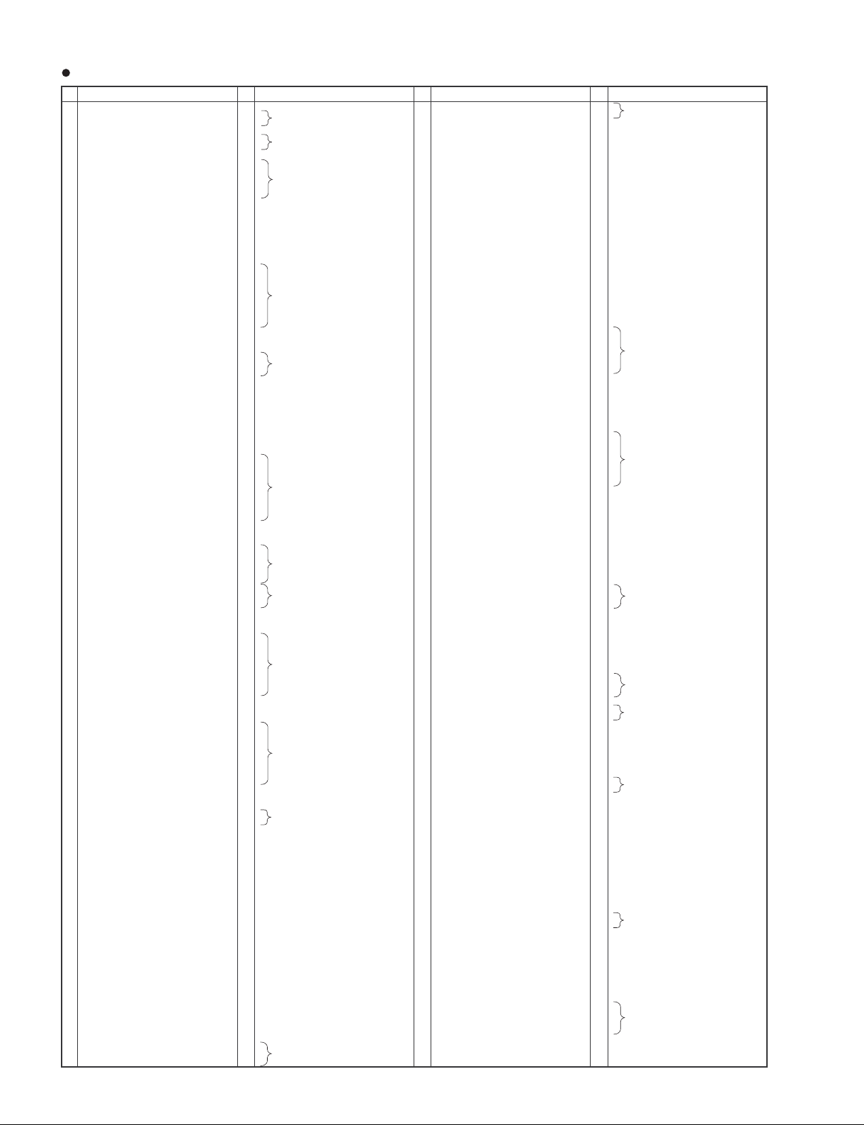
DTXTREME Ⅲ
HD6417727F160C (X2890B00) CPU
24
PIN
NO.
1
2
3
4
5
6
7
8
9
10
11
12
13
14
15
16
17
18
19
20
21
22
23
24
25
26
27
28
29
30
31
32
33
34
35
36
37
38
39
40
41
42
43
44
45
46
47
48
49
50
51
52
53
54
55
56
57
58
59
60
61
62
63
64
65
66
67
68
69
70
71
72
73
74
75
76
77
78
79
80
81
82
83
84
85
86
87
88
89
90
91
92
93
94
95
96
97
98
99
100
101
102
103
104
105
106
107
108
109
110
111
112
113
AFE_RLYCNT_/USB1d_DMNS/PTK[1]
114
115
116
117
PTM[7]/PTINT[7]/AFE_FS/USB1d_RCV
118
PTM[6]/PTINT[6]/AFE_RXIN/USB1d_SPEED
119
PTM[5]/PTINT[5]/AFE_TXOUT/USB1d_TXSE0
120
NAME FUNCTION FUNCTION
Vcc-RTC
XTAL2
EXTAL2
Vss-RTC
MD1
MD2
NMI
IRQ0/IRL0_/PTH[0]
IRQ1/IRL1_/PTH[1]
IRQ2/IRL2_/PTH[2]
IRQ3/IRL3_/PTH[3]
IRQ4/PTH[4]
VEPWC
VCPWC
MD5
/BREQ
/BACK
VssQ
CKIO2
VccQ
D31/PTB[7]
D30/PTB[6]
D29/PTB[5]
D28/PTB[4]
D27/PTB[3]
D26/PTB[2]
D25/PTB[1]
D24/PTB[0]
VssQ
D23/PTA[7]
VccQ
D22/PTA[6]
D21/PTA[5]
D20/PTA[4]
Vss
D19/PTA[3]
Vcc
D18/PTA[2]
D17/PTA[1]
D16/PTA[0]
D15
VssQ
D14
VccQ
D13
D12
D11
D10
D9
D8
D7
D6
VssQ
D5
VccQ
D4
D3
D2
D1
D0
A0
A1
A2
VssQ
A3
VccQ
A4
A5
A6
A7
A8
A9
A10
A11
VssQ
A12
VccQ
A13
A14
A15
A16
A17
A18
A19
A20
VssQ
A21
VccQ
A22
A23
Vss
A24
Vcc
A25
BS_/PTK[4]
RD_
WE0_/DQMLL
WE1_/DQMLU/WE
WE2_/DQMUL/ICIORD_/PTK[6]
VssQ
WE3_/DQMUU/ICIOWR_/PTK{7}
VccQ
RD/WR_
PTE[7]/PCC0RDY/AUDSYNC_
/CS0
/CS2
/CS3
/CS4/PTK[2]
/CS5/CE1A_/PTK[3}
/CS6/CE1B_
CE2A_/PTE[4]
CE2B_/PTE[5]
AFE_HC1/USB1d_DPLS/PTK[0]
VssQ
AFE_SCLK/USB1d_TXDPLS
VccQ
I/O I/O
-
-
-
-
-
-
I
I
I
I
I
O
-
-
-
-
-
-
I/O
I/O
I/O
I/O
I/O
I/O
I/O
I/O
I/O
I/O
I/O
I/O
I/O
I/O
I/O
I/O
-
-
-
-
-
-
-
-
-
-
-
-
-
-
-
-
-
-
-
-
-
-
-
-
-
-
-
-
-
-
-
-
-
-
-
-
-
-
-
-
-
-
-
-
-
-
-
-
-
-
-
-
-
-
O
-
O
O
O
-
O
-
O
O
-
-
-
O
O
O
O
O
O
O
-
I
-
I
I
I
Power supply for RTC (1.9V)
Not in use (XTAL for internal RTC)
Power supply for RTC (0V)
Clock mode setting
Not in use (Non-maskable interrupt request)
External interrupt request
VEE control pin for LCD panel
VCC control pin for LCD panel
Big endian setting
Not in use (bus request)
Bus acknowledge
VssQ
System clock output
VccQ
Data bus
VssQ
Data bus
VccQ
Data bus
Vss
Data bus
Vcc
Data bus
VssQ
Data bus
VccQ
Data bus
VssQ
Data bus
VccQ
Data bus
Address bus
VssQ
Address bus
VccQ
Address bus
VssQ
Address bus
VccQ
Address bus
VssQ
Address bus
VccQ
Address bus
Vss
Address bus
Vcc
Address bus
Not connected (bus cycle start signal)
Read strobe
Write 0 signal
Write 1 signal
Write 2 signal
VssQ
Write 3 signal
VccQ
Read/Write
I/O
Chip Select 0
Chip Select 2
Chip Select 3
Chip Select 4
Chip Select 5
Chip Select 6
Output port (SWP50 Reset)
Output port (PLG Board Reset)
SPD DATA
SPD CL
VssQ
Not in use (USB1 D+ transmission)
VccQ
Not in use
PIN
NO.
PTM[4]/PINT[4]/AFE_RDET_/USB1d_TXDMNS
121
122
123
124
125
126
127
128
129
130
131
132
133
134
135
136
137
138
139
140
141
142
143
144
145
146
147
148
149
150
151
152
153
154
155
156
157
158
159
160
161
162
163
164
165
166
167
168
169
170
171
172
173
174
175
176
177
178
179
180
181
182
183
184
185
186
187
188
189
190
191
192
193
194
195
196
197
198
199
200
201
202
203
204
205
206
207
208
209
210
211
212
213
214
215
216
217
218
219
220
221
222
223
224
225
226
227
228
229
230
231
232
233
234
235
236
237
238
239
240
NAME
Reserved/USB1d_SUSPEND
USB1_ovr_crnt/USBF_VBUS
USB2_ovr_crnt_
RTS2_/USB1d_TXENL
PTE[2]/USB1_pwr_en
PTE[1]/USB2_pwr_en
CKE/PTK[5]
/RAS3/PTJ[0]
Reserved/PTJ[1]
Reserved//CAS/PTJ[2]
VssQ
Reserved/PTJ[3]
VccQ
Reserved/PTJ[4]
Reserved/PTJ[5]
Vss
PTD[5]/CL1
Vcc
PTD[7]/DON
PTE[6]/M_DISP
PTE[3]/FLM
PTE[0]/TDO
PCC0RESET/DRACK0
PCC0DRV_/DACK0_
/WAIT
/RESETM
/ADTRG/PTH[5]
/IOIS16/PTG[7]
/ASEMD0
PTG[5]/ASEBRKAK_
PTG[4]
PCC0BVD2/PTG[3]/AUDATA[3]
PCC0BVD1/PTG[2]/AUDATA[2]
Vss
PCC0CD2/PTG[1]/AUDATA[1]
Vcc
PCC0CD1/PTG[0]/AUDATA[0]
VssQ
PTF[7]/PINT[15]/TRST_
VccQ
PTF[6]/PINT[14]/TMS
PTF[5]/PINT[13]/TDI
PTF[4]/PINT[12]/TCK
PTF[3]/PINT[11]/Reserved
PCCREG_/PTF[2]/Reserved
PCC0VS1_/PTF[1]/Reserved
PCC0VS2_/PTF[0]/Reserved
MD0
Vcc-PLL1
CAP1
Vss-PLL1
Vss-PLL2
CAP2
Vcc-PLL2
PCC0WAIT_/PTH[6]/AUDCK
Vss
Vcc
XTAL
EXTAL
LCD15/PTM[3]/PINT[10]
LCD14/PTM[2]/PINT[9]
LCD13/PTM[1]/PINT[8]
LCD12/PTM[0]
STATUS0/PTJ[6]
STATUS1/PTJ[7]
CL2/PTH[7]
VssQ
CKIO
VccQ
TxD0/SCPT[0]
SCK0/SCPT[1]
TxD_SIO/SCPT[2]
SIOMCLK/SCPT[3]
TxD2/SCPT[4]
SCK_SIO/SCPT[5]
SIOFSYNC/SCPT[6]
RxD0/SCPT[0]
RxD_SIO/SCPT[2]
Vss
RxD2/SCPT[4]
Vcc
SCPT[7]/CTS2_/IRQ5
LCD11/PTC[7]/PINT[3]
LCD10/PTC[6]/PINT[2]
LCD9/PTC[5]/PINT[1]
VssQ
LCD8/PTC[4]/PINT[0]
VccQ
LCD7/PTD[3]
LCD6/PTD[2]
LCD5/PTC[3]
LCD4/PTC[2]
LCD3/PTC[1]
LCD2/PTC[0]
LCD1/PTD[1]
LCD0/PTD[0]
DREQ0_/PTD[4]
LCK/UCLK/PTD[6]
/RESETP
CA
MD3
MD4
/Scan_testen
Avcc_USB
USB1_P
USB1_M
Avss_USB
USB2_P
USB2_M
Avcc_USB
Avss
AN[2]/PTL[2]
AN[3]/PTL[3]
AN[4]/PTL[4]
AN[5]/PTL[5]
Avcc
AN[6]/PTL[6]/DA[1]
AN[7]/PTL[7]/DA[0]
Avss
I
Not in use
O
I
USB function VBUS
-
USB2_HOST2 over current detection
O
Not in use
O
USB1 voltage control
O
USB2 voltage control
O
Enable (SDRAM)
O
RAS for SDRAM
O
Not in use
O
CAS for SDRAM
-
VssQ
O
Output port (DAC Reset)
-
VccQ
O
Output port (SIO Reset)
O
Output port (DAC Mute)
-
Vss
O
LCD line clock
-
Vcc
O
LCD DISPLAY ON
O
LCD alternater
O
LCD frame line marker
O
JTAG (test data output)
O
DMA request acceptance
O
DMA acknowledge
-
Hardware wait request
-
Manual reset request
I
Analog A/D trigger
I
-
Not in use
I
I
I
-
Vss
I
Not in use
-
Vcc
I
Not in use
-
VssQ
I
Not in use
-
VccQ
I
I
I
Not in use
I
I
I
I
-
Clock mode setting
-
Power supply for Vcc_PLL1 - PLL1(1.9V)
-
External capacitance for CAP1 _ PLL1
-
Power supply for Vss_PLL1 _ PLL1(0V)
-
Power supply for Vss_PLL2 _ PLL2 (0V)
-
External capacitance for CAP2 _ PLL2
-
Power supply for Vcc_PLL2 _ PLL2 (1.9V)
I
Not in use
-
Vss
-
Vcc
-
Clock oscillator
-
External clock
I
I
Not in use
I
I
Input port (Flash ROM RY/BY)
O
Output port (Flash ROM write protect)
O
Output port (Flash ROM ACC)
O
LCD clock output
-
VssQ
-
System clock input/output (for SDRAM)
-
VccQ
O
Output port for SCI
O
O
Not in use
O
O
Output port for SCI
O
Not in use
O
i
Receiving data 0
i
Not in use
-
Vss
i
Receiving data 2
-
Vcc
I
Not in use
O
Output port (PLG CLOCK ON/OFF)
O
Not in use
O
-
VssQ
O
Not in use
-
VccQ
O
LCD DATA7
O
LCD DATA6
O
LCD DATA5
O
LCD DATA4
O
LCD DATA3
O
LCD DATA2
O
LCD DATA1
O
LCD DATA0
I
DMA request
I
USB clock
-
Power on reset request
-
Hardware standby request
-
Bus width setting for area0
-
-
Test pin (fixed to 3.3V)
-
USB analog power supply (3.3V)
IO
USB1 data input/output (+)
IO
USB1 data input/output (-)
-
USB analog power supply (0V)
USB2 data input/output (+)
IO
IO
USB2 data input/output (-)
-
USB analog power supply (3.3V)
-
A/D analog power supply (0V)
I
I
AD converter input
I
I
-
A/D analog power supply (3.3V)
I
AD converter input
O
DA converter output (LCD contrast)
-
A/D analog power supply (0V)
DM: IC25
DM2-EL: IC006
AK4393VF-E2 (XW029A00) DAC (Digital to Analog Converter)
PIN
NAME I/O FUNCTION
NO.
1
DVSS
2
DVDD
3
MCLK
4
5
BICK
6
SDATA
7
LRCK
SMUTE//CS
8
9
DEM0/CCLK
10
DEM1/CDTI
11
12
13
14
/PD
DFS
DIF0
DIF1
DIF2
-
I
I
I
I
I
I
I
I
I
I
I
I
Digital ground
Digital power supply
Master clock
Power down mode
Audio serial data clock
Audio serial data input
L/R clock
Soft mute
Double speed sampling mode
De-emphasis enable
Digital input format
PIN
NAME I/O FUNCTION
NO.
15
16
17
18
19
20
21
22
23
24
25
26
27
28
BVSS
VREFL
VREFH
AVD D
AVSS
AOUTR-
AOUTR+
AOUTL-
AOUTL+
VCOM
P//S
CKS0
CKS1
CKS2
I
I
-
O
O
O
O
O
I
I
I
I
IC BLOCK DIAGRAM(IC ブロック図)
DTXTREME Ⅲ
DMSUB: IC116 ‒118
PN: IC706, 707
Substrate ground
Low level voltage reference
High level voltage reference
Analog power supply +5 V
Analog ground
Rch negative analog output
Rch positive analog output
Lch negative analog output
Lch positive analog output
Common voltage output
Parallel/serial select
Master clock select
SN74LV04APWR (X5965A00)
DMSUB: IC115
Hex Inverter
Vss
1
1A
2
1Y
3
2A
4
2Y
5
3A
6
3Y
7
14
VDD
13
6A
12
6Y
11
5A
10
5Y
9
4A
8
4Y
SN74LV32APWR (X5647A00)
JK: IC351
TC74HCT32AF (XY096A00)
DM: IC15
Quad 2 Input OR
1
1A
2
1B
3
1Y
42A
52B
62Y
7GND
14
13
12
11 4Y
10 3B
9 3A
8 3Y
Vcc
4B
4A
TC74VHC08F (XT014B00)
DM: IC18
Quad 2 Input AND
1
VSS
1A
2
1B
1Y
3
42A
52B
62Y
7
14
13
12
11 4Y
10 3B
9 3A
8 3Y
VDD
4B
4A
SN74AHCT125PWR (X4152A00)
DM: IC13
Quad 3-State Bus Buffer
1
GND
C1
2
A1
3
Y1
4
C2
5
A2
6
Y2
7
14
Vcc
13
C4
12
A4
11
Y4
10
C3
9
A3
8
Y3
TC74VHC14FT (XV890B00)
DM: IC8, 14
Hex Inverter
GND
1
1A
2
1Y
3
2A
4
2Y
5
3A
6
3Y
7
14
VDD
13
6A
12
6Y
11
5A
10
5Y
9
4A
8
4Y
SN74LV126APWR (X3865A00)
DM: IC17
Bus Buffer
GND
1
1G
2
1A
3
2Y
4
2G
5
2A
6
2Y
7
14
Vcc
13
4G
12
4A
11
4Y
10
3G
9
3A
8
3Y
25
DTXTREME Ⅲ
HD74LVC139FPEL (XS048A00)
DM: IC23
Dual 2 to 4 Demultiplexer
1Y0
1Y1
1Y2
1Y3
GND
1
1G
G
2
1A
A
3
B
1B
4
Y0
5
Y1
6
Y2
7
Y3
8
16
Vcc
G
15
2G
A
14
2A
B
13
2B
Y0
12
2Y0
Y1
11
2Y1
Y2
10
2Y2
Y3
9
2Y3
DS90LV011ATMF/NOPB (X6788A00)
DMSUB: IC122
3V LVDS Single High Speed Differential Driver
SN74LV245APWR (X3693A00)
DMSUB: IC121 JK: IC349, 350, 352354
SN74LVC245APWR (XZ287A00)
DM: IC6, 10‒12, 16, 19, 20
TC74VHCT245AFT (XT744B00)
SN74LV4052APWR (X6976A00)
JK: IC338, 339
Differential 4-Channel
Multiplexer/Demultiplexer
PN: IC711
Octal 3-State Bus Transceiver
1D1R
2
A1
A2
3
A3
4
A4
5
A5
6
A6
7
A7
8
A8
9
GND
10
DS90LV012ATMF/NOPB (X6789A00)
PN: IC713
3V LVDS Single CMOS Differential Line Receiver
CC
V
20
G
19
B1
18
B2
17
B3
16
B4
15
B5
14
B6
13
B7
12
B8
11
AM26LS31CNSR (XU996A00)
DMSUB: IC113
Quad Line Driver
Y-C OM
INH
VEE
VSS
1
0Y
2
2Y
2Y
3
Y-C OM
4
3Y
3Y
5
1Y
1Y
6
INH
7
8
0Y
X-COM
B
16
VDD
15
2X
2X
14
1X
1X
13
X-COM
12
0X
0X
11
3X
3X
10
A
A
B
9
1 5
VDD
GND
OUT −
D
2
3
4
TTL IN
OUT +
NJM2068MD-T2 (X3505A00)
PN: IC703, 708, 709, 714, 715
NJM4556AD (XQ824A00)
PN: IC701
Dual Operational Amplifier
+DC Voltage
+-
+-
8
Supply
7
Output B
Inverting
6
Input B
Non-Inverting
5
Input B
Output A +V
Inverting
Input A
Non-Inverting
Input A
-DC Voltage Supply
1
2
3
4-V
1 5
VDD
2
GND
3 4
IN +
R
TTL OUT
IN −
NE5532DR (X5482A00)
PN: IC704
NJM2903M(TE1) (X5814A00)
NJM2904M (XV190A00)
JK: IC301306, 321324, 329333, 335337
Dual Operational Amplifier
+-
+DC Voltage
8
Supply
Output B
7
Inverting
6
Input B
Non-Inverting
5
Input B
1
Output A +V
Inverting
2
Input A
Non-Inverting
Input A
Ground
3
4
+-
1
1A
2
1Y
3
1Z
ENABLE G
A
H
L
H
L
X
4
5
2Z
6
2Y
7
2A
8
GND
ENABLESINPUT
GGY Z
H
H
X
X
L
X
X
L
L
H
OUTPUTS
H
L
H
L
Z
16
Vcc
15
4A
14
4Y
13
4Z
12
ENABLE G
11
3Z
10
3Y
3A
9
L
H
H= high level
L
L= low level
H
X= irrelevant
Z
Z= high impedance (off)
NJM2114M(TE1) (XS537B00)
DMSUB: IC105-107 PN: IC710
Dual Operational Amplifier
A Output
-
Input
A
A +Input
1
2
+-
3
-
V
+-
4
+
V
+V
8
B Output
7
B
-
Input
6
B +Input
5
26
DTXTREME Ⅲ
LM3525MX-H/NOPB (X3119A00)
DM: IC28
USB Power Switch
7
FLAG
IN
2
1EN
Pin Function
Shutdown
FLAG
GND
NC
EN
Pin No.
1
2
3
4, 5
7
6, 8
1
2
3
4
8
OUT
IN
7
OUT
6
5
NC
Pin Name
EN
Enable (Input): Logic-compatible enable input.
(LM3525-L)
EN
(LM3525-H)
FLG
Fault Flag (Output): Active-low, open-drain output. Indicates overcurrent, UVLO,
and thermal shutdown.
GND
Ground
NC
Not internally connected.
IN
Supply Input: Input to the power switch and the supply voltage for the IC.
OUT
Switch Output: Output of the high side switch. Pins 6 and 8 must be tied together.
LTC1773EMS (X3215A00)
DMSUB: IC103
DC-DC CONVERTER
Error
Detect
and
Control
FET
Drive
SYNC/FCB
8 OUT
3
0.4μA
LTC1144CS8 (X9457A00)
DMSUB: IC127
Voltage Converter -12V
1
BOOST
+
2
CAP
3
GND
-
4
CAP
Y Y= “0” ONLY WHEN X IN A CONSTANT “1”
BURST
DEFEAT
X
OSC
Pin No.
SLOPE
COMP
8
7
6
5
Pin Name
1
BOOST
2
CAP
3
GND
4
CAP
6
V
OUT
5
SHDN
7
OSC
+
8
V
+
V
(8)
+
V
OSC
BOOST
10X
SHDN
V
+
-
(1)
OSC
OSC
OUT
(7)
SHDN
(6)
This pin will raise the oscillator frequency by a factor of 10 tied high.
Positive Terminal for Pump Capacitor
Ground Reference
Negative Terminal for Pump Capacitor
Output of the Converter
Shutdown Pin
Oscillator Input Pin
Input Voltage
Pin Function
SW1
φ
2
÷
φ
0.4V
SW2
+
CAP
(2)
+
C1
CAP
GND
-
(4)
(3)
8
V
9
SENSE
V
OUT
(5)
+
C2
IN
–
0.6V
SYNC
4
DEFEAT
0.8V REF
UVLO
TRIP = 2.5V
SHUTDOWN
RUN/SS
SYNC/FCB
GND
1
I
TH
2
3
4
V
FB
5
10
SW
9
8
7
6
SENSE
V
IN
TG
BG
–
V
FB
RUN/SS
CIRCUIT BOARDS(シート基板図)
DM Circuit Board (X3164G0) ............................................................... 28/30
DMSUB Circuit Board (X9380C0) .......................................................32/34
JK Circuit Board (X9365C0) ................................................................ 36/38
PN Circuit Board (X9385C0/ X9385D0) ............................................... 40/42
FREQ
SHIFT
2
1.5μA
0.86V
0.8V
0.8V
EA
UVLO
TRIP = 2.5V
OVDET
SYNC
DEFEAT
0.22V
EN
SLEEP
I
AND
COMP
ANTI
SHOOT-THRU
I
RCMP
7
TG
6
BG
10
SW
5
GND
50mV
BURST
COMP
SQ
R Q
SWITCHING
LOGIC
BLANKING
CIRCUIT
1
I
TH
Note: See parts list for details of circuit board component parts.
注 : シートの部品詳細はパーツリストをご参照ください。
27
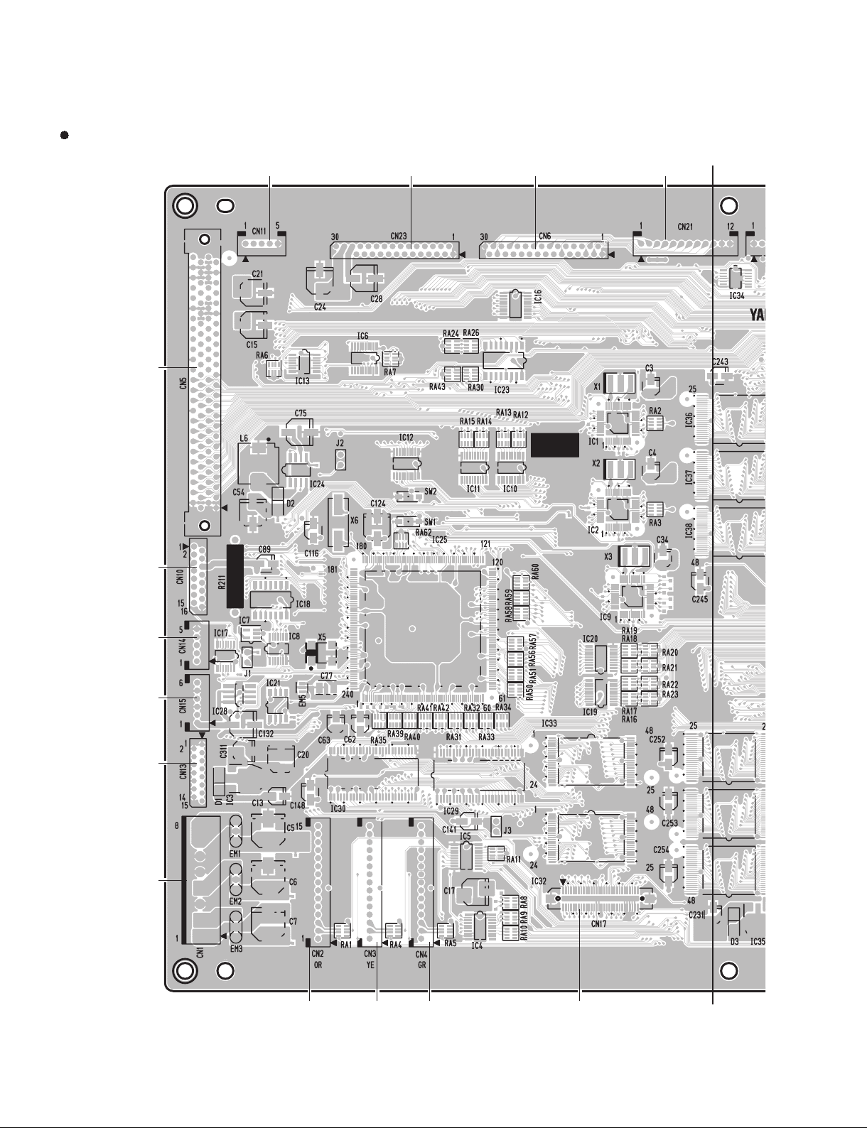
DTXTREME Ⅲ
DM Circuit Board
to DMSUB-CN107
to DMSUB-CN113 to DMSUB-CN111 to DMS
not installed not installed
A
to PN-CN704
to DMSUB-CN104
to DMSUB-CN103
to JK-CN301
to DMSUB-CN102
28
not installednot installednot installednot installed
A’
2NA-WJ91030-1
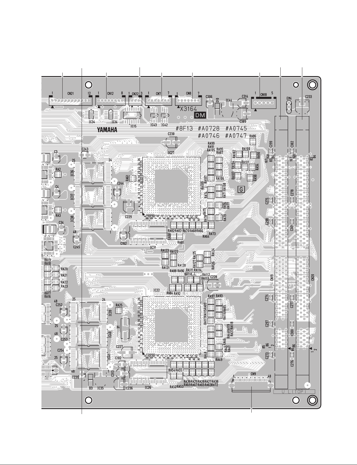
DTXTREME Ⅲ
not installed
A
to DMSUB-CN110 to DMSUB-CN101
not installed
to PN-CN701
not installed
DIMM socket DIMM socket
2NA-WJ91030-1
A’
not installed
Component side
(部品側)
29
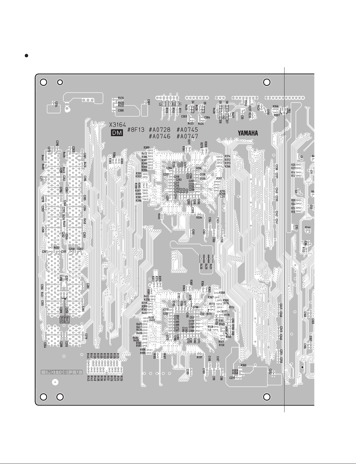
DTXTREME Ⅲ
DM Circuit Board
B
30
B’
2NA-WJ91030-2
 Loading...