HF & V/UHF Band
STEP
VFO/MR
F
A
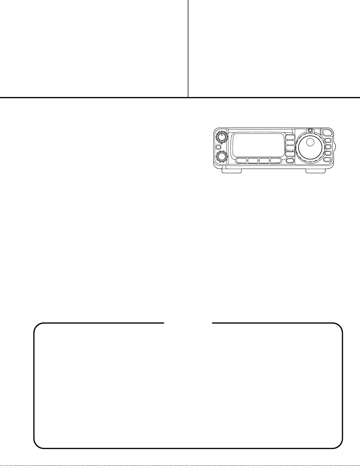
All Mode Mobile Transceiver
FT-100/-100D
Technical Supplement
©2003 VERTEX STANDARD CO., LTD. E089890A
Introduction
This manual provides technical information necessary
for servicing the Yaesu FT-100/-100D HF & V/UHF-Band
Transceiver. It does not include information on installation and operation, which are described in the FT-100/100D Operating Manual provided with the transceiver,
or on accessories which are described in their manuals.
The FT-100/-100D is carefully designed to allow the
knowledgeable operator to make nearly all adjustments
required for various station conditions, modes and operator preferences simply from the controls on the panels,
without opening the case of the transceiver. The FT-100/100D Operating Manual describes these adjustments, plus
certain internal settings.
Servicing this equipment requires expertise in handling
surface mount chip components. Attempts by unqualified
persons to service this equipment may result in permanent damage not covered by warranty. For the major circuit boards, each side of the board is identified by the type
of the majority of components installed on that side. In
most cases one side has only chip components, and the
other has either a mixture of both chip and lead compo-
VERTEX STANDARD CO., LTD.
4-8-8 Nakameguro, Meguro-Ku, Tokyo 153-8644, Japan
VERTEX STANDARD
US Headquarters
10900 Walker Street, Cypress, CA 90630, U.S.A.
International Division
8350 N.W. 52nd Terrace, Suite 201, Miami, FL 33166, U.S.A.
YAESU EUROPE B.V.
P.O. Box 75525, 1118 ZN Schiphol, The Netherlands
YAESU UK LTD.
Unit 12, Sun Valley Business Park, Winnall Close
Winchester, Hampshire, SO23 0LB, U.K.
VERTEX STANDARD HK LTD.
Unit 5, 20/F., Seaview Centre, 139-141 Hoi Bun Road,
Kwun Tong, Kowloon, Hong Kong
MODE
L
F
Q
S
R
/
C
L
A
R
E
L
C
E
T
S
U P
DWN
FUNC
DSP
DCBA
PWR
HOME
LOCK
nents (trimmers, coils, electrolytic capacitors, packaged
ICs, etc.), or lead components only.
While we believe the technical information in this manual is correct, VERTEX STANDARD assumes no liability
for damage that may occur as a result of typographical or
other errors that may be present. Your cooperation in
pointing out any inconsistencies in the technical information would be appreciated. VERTEX STANDARD reserves
the right to make changes in this transceiver and the alignment procedures, in the interest of technological improvement, without notification of owners.
Contents
Specification................................................... 2
Exploded View & Miscellaneous Parts ..... 3
Alignment ....................................................... 5
Block Diagram ............................................. 17
Interconnection Diagram ........................... 18
Board Unit (Schematics, Layouts & Parts)
MAIN Unit.............................................................. 19
6m-FILTER Unit ..................................................... 49
BPF Unit .................................................................. 51
HPF Unit ................................................................. 55
AUDIO-FILTER Unit............................................ 59
LOCAL Unit ........................................................... 63
REF Unit ................................................................. 75
PA Unit ................................................................... 77
LPF Unit.................................................................. 89
DISPLAY Unit........................................................ 99
CNTL Unit ............................................................ 107
CONNECT-1 Unit ............................................... 117
VR Unit ................................................................. 118
CONNECT-2 Unit ............................................... 119
Option ......................................................... 120
TCXO-8 ................................................................. 120
FTS-27 ................................................................... 121
1

Specifications
General
Frequency Range:
Receive 100 kHz – 970 MHz (European version)
100 kHz – 824 MHz, 849 – 864 MHz,
and 894 – 961 MHz (U.S.A version)
Transmit 160 – 6 Meters
2 Meters
70 Centimeters (Amateur bands only)
5167.5 kHz: Alaska Emergency Frequency
(U.S.A. version only)
Emission Modes:
A1 (CW), A3 (AM), A3J (LSB/USB),
F1 (9600 bps Packet), F2 (1200 bps Packet), F3 (FM)
Synthesizer Steps (Min.):
1.25 Hz (CW/SSB), 100 Hz (AM), 100 Hz (FM),
1 kHz (FM)
Antenna Impedance:
50W, Unbalanced
Operating Temp. Range:
–10 °C to +60 °C (14 °F to 122 °F)
Frequency Stability:
Better than ±4 ppm (–10 °C to +50 °C) (SSB/CW/AM)
Better than ±{1 kHz +4 ppm} (FM)
Power Requirements:
DC 13.8V ± 10%, Negative Ground
Current Consumption:
Receive (Squelched): 1.2A, Receive (Max. Audio): 1.6A
Transmit: 22A (@ 100W RF output)
Case Size:
160(W) x 54(H) x 205(D) mm (6.3” x 2.2” x 8.0” WHD)
Weight:
3 kg. (6.6 lb.)
Transmitter
Power Output:
160 – 6m:100 Watts (25 Watts AM carrier)
2m: 50 Watts (12.5 Watts AM carrier)
70cm: 20 Watts (5 Watts AM carrier)
Modulation Types:
SSB: Balanced Modulator
FM: Variable Reactance
AM: Early Stage (Low Level)
FM Maximum Deviation:
±5 kHz (±2.5 kHz on FM-N)
Spurious Radiation:
Harmonics: At least 40 dB down (1.8 – 29.7 MHz)
At least 60 dB down (50/144/430 MHz)
Non-harmonic: At least 50 dB down (1.8 – 29.7 MHz)
At least 60 dB down (50/144/430 MHz)
Carrier Suppression:
At least 40 dB
Opp. Sideband Suppression:
At least 50 dB
SSB Frequency Response:
400 Hz – 2600 Hz (–6 dB)
Microphone Impedance:
200W – 10kW (Supplied microphone: 2kW)
Receiver
Sensitivity:
SSB/CW AM-N FM
100 kHz – 150 kHz: – – –
150 kHz – 250 kHz*: 5 µV 40 µV –
250 kHz – 1.8 MHz*: 4 µV 32 µV –
1.8 – 28 MHz*: 0.25 µV 2 µV –
28 – 30 MHz: 0.25 µV 2 µV 0.50 µV
50 – 54 MHz: 0.20 µV 2 µV 0.50 µV
144/430 MHz: 0.125 µV 2 µV 0.20 µV
Above specifications are worst-case.
SSB/CW/AM-N figures are for 10 dB S/N, 12 dB SINAD
on FM. *: IPO off
Squelch Sensitivity:
SSB/CW/AM FM
1.8 – 28 MHz: 2.5 µV –
28 – 30 MHz: 2.5 µV 0.32 µV
50 – 54 MHz: 1.12 µV 0.20 µV
144/430 MHz: 0.8 µV 0.16 µV
Intermediate Frequencies:
1st IF: 68.985 MHz (SSB/CW/FM/Digital)
67.980 MHz (W-FM)
2nd IF: 11.705 MHz (SSB/CW/FM/Digital)
10.700 MHz (W-FM)
3rd IF: 455 kHz (FM)
Image Rejection:
Better than 70 dB (1.8 – 30 MHz, 50 – 54 MHz)
Better than 60 dB (144 – 148 MHz, 430 – 440 MHz)
IF Rejection:
Better than 70 dB (1.8 – 30 MHz)
Better than 60 dB (50 – 54 MHz, 144 – 148 MHz,
430 – 440 MHz)
Selectivity (–6/–60 dB):
SSB/CW: 2.2 kHz/5.2 kHz
CW: 450 Hz/1.8 kHz
(FT-100: Optional XF-117C installed)
CW-N: 250 Hz/1.2 kHz
(Optional XF-117CN installed)
AM: 5.2 kHz/18 kHz
(Optional XF-117A installed)
FM: 15 kHz /25 kHz (–6/–50 dB)
Audio Output:
At least 1.5W into 8W @ 10% THD
Audio output impedance:
4W – 8W
Specifications are subject to change without notice, and are guaran-
teed within amateur bands only.
2
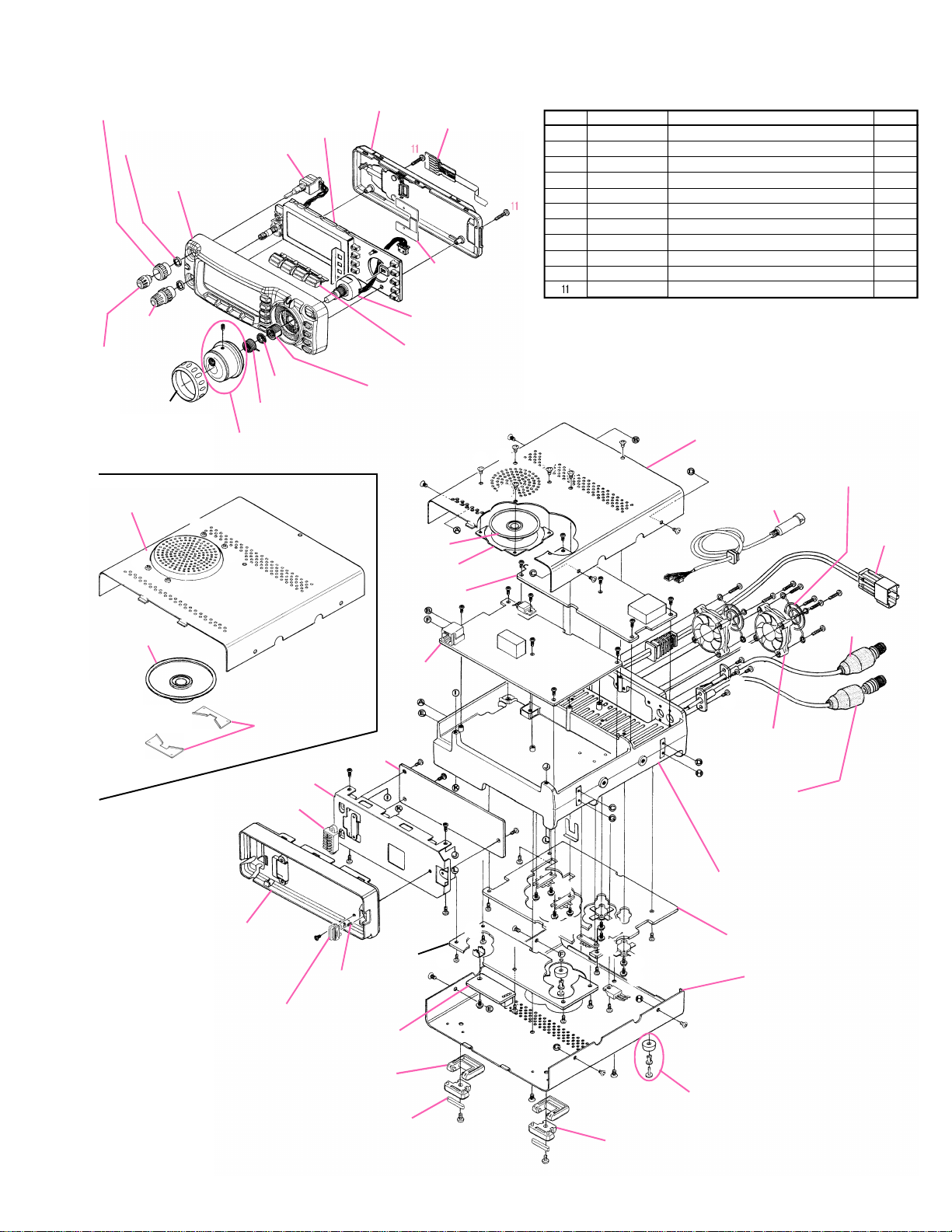
Exploded View & Miscellaneous Parts
KNOB (SQL)
RA0067900
SPECIAL NUT (X2 pcs)
R6054387B
FRONT PANEL ASS'Y
RA0066600
KNOB (SELECT)
RA0067700
KNOB (AF)
RA0067800
RUBBER RING
RA0068200
TOP CASE (FT-100D)
CS1616002
É
É
É
SPEAKER
M4090146
VR Unit
WASHER
R3135000A
COIL SPRING
R0135010A
KNOB MAIN ASS'Y
RA0068000
É
HOLDER
RA0254400
FRONT FRAME
RA0068600
Connect-1 Unit
Display Unit
CNTL Unit
Æ
REAR PANEL
RA0068400
À
ROTARY ENCODER
Q9000709
Q9000709A (Lot.26-)
KNOB (FUNC)
RA0067400
RA006740A (Lot.3-)
NUT
R6144801
È
SPEAKER
M4090135
HOLDER
R0150630
LPF Unit
MAIN Unit
Å
Connect-2 Unit
HOLDER PLATE
RA0069500
È
É
É
Æ
Æ
Å
Æ
É
REF. VXSTD P/N
À
É
Æ
Æ
Æ
Æ
Æ
Å
Description
À
Á
Â
Ã
Ä
Å
Æ
Ç
È
É
À
U02308001
U03306001
U07430107
U20318007
U20406007
U24204001
U24206001
U31203007
U31206007
U34206001
U43112007
SEMS SCREW SM3x8
SEMS SCREW ASM3x6
PAN HEAD SCREW M2.6x3B
BINDING HEAD SCREW M3x18B
BINDING HEAD SCREW M4x6B
TAPTITE SCREW M2.6x4
TAPTITE SCREW M2.6x6
OVAL HEAD SCREW M2.6x3B
OVAL HEAD SCREW M2.6x6B
TAPTITE SCREW M2.6x6
TAPTITE SCREW M2x12B
Non-designated parts are available only as
part of a designated assembly.
TOP CASE
CS1616001
È
È
CT CABLE
T9101492A
È
È
Æ
Ã
ÃÃÃ
Æ
Æ
Æ
Ç
Ç
Ç
Ç
FAN (X2 pcs)
M2090024
M2090024A (Lot.3-)
M2090035 (Lot.28-)
WIRE ASS'Y
T9206740 (USA)
T9206741 (EXPORT, AUSTRALIA)
Qty.
10
1
1
8
2
3
25
4
12
4
2
FAN GUARD (X2 pcs)
S5000206
DC CABLE
T9206750
Ã
Ã
Ã
WIRE ASS'Y
T9206740
Ã
SUB PANEL
RA006850C
Æ
Â
Local Unit
COIL SPRING
R0137551
RELEASE KNOB
RA0069600
STAND (X2 pcs)
R3086910C
SPONGE RUBBER (X2 pcs)
R7088070A
REF Unit
È
Æ
Æ
Ä
Á
Æ
Æ
È
Æ
Æ
È
À
Ä
À
À
À
Æ
Æ
È
À
À
À
À
Æ
Æ
È
FOOT (X2 pcs)
R3086890B
CHASSIS
RA0061100
Æ
È
CASE LEG (X2 pcs)
S4000043
PA Unit
BOTTOM CASE
CS1617001
3
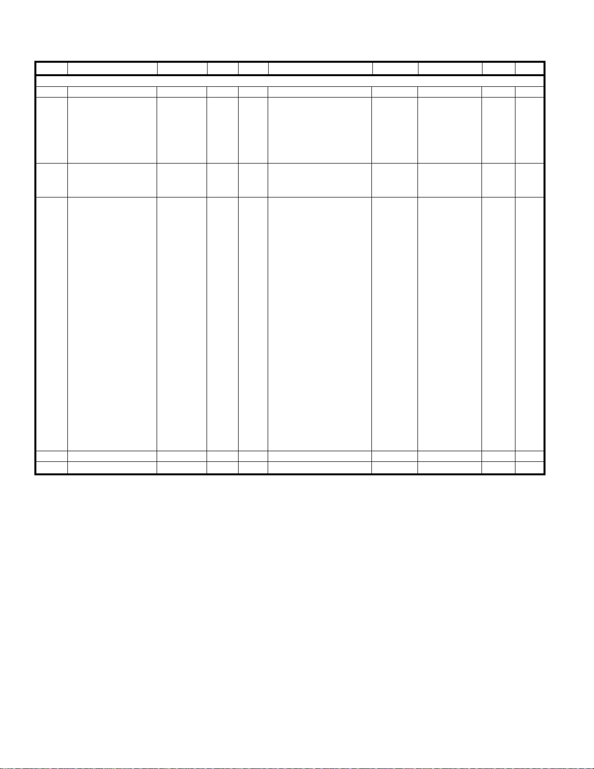
Exploded View & Miscellaneous Parts
DESCRIPTION VALUE V/W TOL. YAESU P/NMFR’S DESIG VERS.REF. LOT. SIDE
*** MAIN ASSY ***
C 0001 AL.ELECTRO.CAP. 100uF 16V SMG1CVB101M 100UF K40129060 2FN0001 FAN JF0410S1HB-086 DC12V M2090024 1FN0001 FAN JF0410S1HB-175 DC12V M2090024A 3FN0001 FAN KF0410S1H-175 DC12V M2090035 28FN0002 FAN JF0410S1HB-086 DC12V M2090024 1FN0002 FAN JF0410S1HB-175 DC12V M2090024A 3FN0002 FAN KF0410S1H-175 DC12V M2090035 28L 0001 TOROIDAL CORE ESD-R-12C L9190069 2L 0002 FERRITE BEADS FSOC171RT01B L9190116 2L 0003 FERRITE BEADS ESD-FPL-13 L9190114 2P 0001 WIRE ASSY A0898 #241890 T9206734 1P 0003 WIRE ASSY A0898 #241891 T9206735 1P 0005 WIRE ASSY A0898 #241892 T9206736 1P 0007 WIRE ASSY A0898 #241888 T9206732 1P 0009 WIRE ASSY A0898 #241887 T9206731 1P 0011 WIRE ASSY A0898 #241889 T9206733 1P 0013 WIRE ASSY A0898 T9206744 1P 0014 CT CABLE 8P-4PX2 530MM T9101492 1P 0014 CT CABLE 8P-4PX2 530MM T9101492A 2P 0016 WIRE ASSY A0898 M T9206740 USA 1P 0016 WIRE ASSY A0898 N T9206741 EXPORT 1P 0016 WIRE ASSY A0898 N T9206741 AUSTRALIA 1P 0017 WIRE ASSY A0898 M T9206740 1P 0018 WIRE ASSY A0898 T9206750 1P 0101 WIRE ASSY GRA 240 TMP/TMP T9309401 1P 0101 WIRE ASSY GRA 235 TMP/TMP T9318095 2P 0103 WIRE ASSY RED 290 TMP/TMP T9311404 1P 0103 WIRE ASSY RED 265 TMP/TMP T9318096 2P 0105 WIRE ASSY GRA 200 TMP/TMP T9311403 1P 0107 WIRE ASSY ORG 210 TMP/TMP T9317850 1P 0109 WIRE ASSY RED 300 TMP/TMP T9311408 1P 0111 WIRE ASSY RED 170 TMP/TMP T9318092 2P 0113 WIRE ASSY GRA 138 TMP/TMP T9318097 2S 0001 ROTARY ENCODER RES20D50-201-1D Q9000709 1SP0001 SPEAKER VS-50-0827B 1.5W/8-OHM M4090135 2-
4

Alignment
Introduction and Precautions
The following procedures cover adjustments that are
not normally required once the transceiver has left the factory. However, if damage occurs and some parts subsequently are replaced, realignment may be required. If a
sudden problem occurs during normal operation, it is likely due to component failure; realignment should not be
done until after the faulty component has been replaced.
We recommend that servicing be performed by authorized Yaesu service technicians, who are experienced with
the circuitry and fully equipped for repair and alignment.
If a fault is suspected, contact the selling dealer for instructions regarding repair. Authorized Yaesu service
technicians have the latest modification information, and
realign all circuits and make compete performance checks
to ensure compliance with the factory specifications after
repairs.
Those who do undertake any of the following alignments are cautioned to proceed at their own risk. Problems caused by unauthorized attempts at realignment are
not covered by the warranty policy. Also, Yaesu must reserve the right to change circuits and alignment procedures, in the interest of improved performance, without
notifying owners. Under no circumstances should any
alignment be attempted unless the normal function and
operation of the transceiver are clearly understood, the
cause of the malfunction has been clearly pinpointed and
any faulty components replaced, and the need for realignment determined to be absolutely necessary.
The following test equipment (and thorough familiarity with its correct use) is necessary for complete realignment. Correction of problems caused by misalignment
resulting from unauthorized adjustments made with improper test equipment is not covered by warranty. Although most steps do not require all of the equipment listed, the interaction of some adjustments may require that
more complex adjustments be performed afterwards. Do
not attempt to perform only a single step unless it is clearly isolated electrically from all other steps. Rather, have
all test equipment ready before beginning, and follow all
of the steps in a section in the order they are presented.
Required Test Equipment
m Digital DC Voltmeter (high-Z, 1 MW/V)
m DC Ammeter
m AC Voltmeter
m RF Standard Signal Generator w/ calibrated output and
dB scale, 0 dBµ = 0.5 µV
m AF Signal Generator with calibrated output
m Frequency Counter
m 50- W Dummy Load (150 ~ 250 watts)
m 50- W Resistor, 1 Watt (low-power dummy load for cir-
cuit termination)
m 16.6- W Dummy Load (150 watts)
m In-Line Wattmeter (150 ~ 250 watts, 50-W)
m Linear Detector
m RF Attenuator (150 watts, 50 dB) or sampling coupler
m Spectrum Analyzer good to at least 1 GHz
m SINAD Meter
Alignment Preparation & Precautions
A 50-W dummy load and in-line wattmeter must be connected to the antenna jack in all procedures that call for
transmission, except where specified otherwise. Correct
alignment is not possible with an antenna. Except where
specified otherwise, the transceiver should be tuned to
14.2000 MHz, USB mode, and these controls set as indicated:
m AF fully CCW
m SQL/RF fully CCW
The transceiver’s Alignment Routine is required for
some procedures. If an Alignment Routine cannot be selected, power may have to be switched off then back on to
re-enable menu selection.
To begin, turn the transceiver off. Press the A, B, and C
keys together while turning the transceiver on again, then
press and hold the FUNC key.
In the alignment procedure, each alignment parameter
is selected by rotating the main DIAL. To exit the alignment routine, press the FUNC key. After performing the
system alignment in its entirety, individual settings can
be returned to and adjusted should the need arise.
Read each step to determine if the same test equipment
used in the previous step will be required. If not, remove
the test equipment (except dummy load and wattmeter, if
connected) before proceeding. Correct alignment requires
that the ambient temperature be the same as that of the
transceiver and test equipment, and that this temperature
be held constant within 68 ~ 86°F (20 ~ 30°C). If the transceiver is brought into the shop from hot or cold air, it
should be allowed time for thermal equalization with the
environment before alignment. Alignments must only be
made with oscillator shields and circuit boards firmly affixed in place. Also, the test equipment must be thoroughly
warmed up before beginning.
Notes: Signal levels in dB referred to in alignment are based on
0 dBµ = 0.5 µV (closed circuit).
Table Note: DC voltages should be within ±10 % of those listed
in the voltage tables.
5
Alignment
Local Oscillator Adjustments
Reference Frequency Adjustment
m Remove the coaxial plug from J2005 and connect the
frequency counter across its socket.
m Adjust trimmer capacitor TC2801 or X2901 (use TCXO-
8) for 57.279999 MHz ± 60 Hz or 30 Hz (use TCXO-8)
on the frequency counter.
m Disconnect the frequency counter, and replace the plug
into J2005.
2nd Local Adjustment
m Connect the 50-W resistor and RF millivoltmeter to
J2005.
m Adjust T2003 and T2004 for maximum indication on
the RF millivoltmeter (at least 180 mV).
m Disconnect the frequency counter, and replace the plug
into J2005.
3rd Local Adjustment
m Set the RF power to the minimum (using Menu #21),
and select the CW mode. Connect the 50-W resistor and
RF millivoltmeter to J2004.
m Key the transmitter, and adjust T2001 and T2002 for
maximum indication on the RF millivoltmeter (at least
80 mV).
m Replace the RF millivoltmeter with the frequency
counter, and confirm that the local frequency is 11.705
MHz (±1 kHz) on the frequency counter.
m Disconnect the frequency counter, and replace the plug
into J2004.
PLL Adjustments
VCO VCV Adjustment
m Connect the DC voltmeter to TP2001, and referring to
table below, tune the transceiver to each frequency listed. Then confirm that the correct voltage is present, or
adjust the listed component for the required voltage.
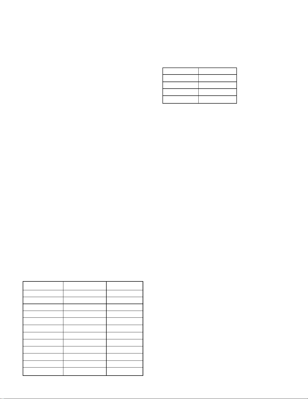
Tune to: Adjust/Confirm For
449.99999 MHz Adjust TC2005 7.4 V ±0.1 V
420.00000 MHz Confirm 2.0 V ~ 4.8 V
381.99999 MHz Adjust TC2006 7.4 V ±0.1 V
108.00000 MHz Confirm 1.2 V ~ 4.0 V
245.99999 MHz Adjust TC2004 7.4 V ±0.1 V
60.00000 MHz Confirm 0.8 V ~ 4.0 V
197.99999 MHz Adjust TC2003 7.4 V ±0.1 V
33.00000 MHz Confirm 1.2 V ~ 4.0 V
170.99999 MHz Adjust TC2002 7.4 V ±0.1 V
15.00000 MHz Confirm 1.4 V ~ 4.2 V
14.99999 MHz Adjust TC2001 7.4 V ±0.1 V
0.03000 MHz Confirm 1.5 V ~ 4.0 V
6
1st Local Output Level
m With the 50-W resistor and RF millivoltmeter connect-
ed to the J2003, and referring to table below, tune the
transceiver to each frequency listed, then confirm that
the required output level is present at the listed frequency.
Tune to: For
14.175 MHz 11 dBm ±3 dB
52.050 MHz 11 dBm ±3 dB
146.500 MHz 11 dBm ±3 dB
440.500 MHz 11 dBm ±3 dB
PA Unit Adjustments
Before beginning, remove the coaxial plugs from J3503
and J3005, and connect 50-W resistors across the sockets
for these jacks (shunt to ground at each jack).
HF/50MHz Driver Section Idling Current
m Remove the coaxial plug from J3001, and connect a 50-W
resistor across its socket. Remove the jumper connector at J3504. Connect the ammeter to J3504 (pin 1: “–”
lead, pin 2: “+” lead).
m Tune the transceiver to the 14.2000 MHz and select the
USB mode.
m Key the transmitter, and adjust VR3004 for a reading of
50 ~ 55 mA on the ammeter.
m Disconnect the ammeter, and reinstall the jumper con-
nector at J3504.
m Remove the jumper connector at J3003. Connect the am-
meter to J3003 (pin 1: “–” lead, pin 2: “+” lead).
m Key the transmitter, and adjust VR3001 for a reading of
1.1 A on the ammeter (within 60 mA).
m Disconnect the ammeter, and reinstall the jumper con-
nector at J3003.
HF/50 MHz Final Idling Current Adjustment
m Leave the coaxial plug disconnected from J3001, and
be sure that the 50-W resistor is connected across its
socket. Connect the ammeter between the transceiver’s
13.8VDC connector and the DC power supply.
m Tune the transceiver to the 14.2000 MHz and select USB
mode.
m Key the transmitter, and adjust VR3002 for a reading of
1.6 A on the ammeter (within 50 mA).
m Adjust the VR3003 for a reading of 2.1 A (±50 mA) on
the ammeter.
VHF/UHF Driver Section Idling Current
m Remove the coaxial plug from J3501, and connect a 50-W
resistor across its socket. Remove the jumper connector at J3502. Connect the ammeter to J3502 (pin 1: “–”
lead, pin 2: “+” lead).

Alignment
m Tune the transceiver to the 144.5000 MHz, and select
the USB mode.
m Key the transmitter, and adjust VR3501 for 1.5 ~ 1.6 A
on the ammeter.
m Disconnect the ammeter, and reinstall the jumper con-
nector at J3502.
VHF/UHF Final Idling Current Adjustment
m Leave the coaxial plug disconnected from J3501, and
be sure that the 50-W resistor is connected across its
socket. Connect the ammeter between the transceiver’s
13.8VDC connector and the DC power supply.
m Tune the transceiver to 144.5000 MHz, and select the
USB mode.
m Key the transmitter, and adjust VR3502 for 2.3 A ±0.1 A
on the ammeter.
m Disconnect the ammeter, and reinstall the jumper con-
nector at J3501.
TX and RX IF Adjustments
HF Band RX IF Sensitivity (Coarse Adjust)
m Preset “Alignment” Menu items F-03 [HF RX IF G], F-
04 [50 RX IF G], F-05 [144 RX IF G], and F-06 [430 RX IF
G] to “194” if they are not already set to that value.
m Connect the RF signal generator to the HF/50MHz an-
tenna jack, and connect a 4-W speaker and AC voltmeter to the EXT SP jack.
m Set the transceiver to 14.10000 MHz, and select the USB
mode. Inject a signal from the signal generator to
14.10000 MHz so as to get a reading on the AC voltmeter.
m Adjust T1023, T1025, T1027, T1028, T1030, T1032 ~
T1037, and T1039 in succession several times for maximum indication on the AC voltmeter.
1st Mixer Balance
m Tune the transceiver to 14.10000 MHz, but inject no sig-
nal to the antenna jack.
m Adjust VR1001 for minimum noise output from the
speaker.
HF/50 MHz Band RX IF Sensitivity
m Connect the RF signal generator to the HF/50MHz an-
tenna jack, and leave the 4-W speaker and AC voltmeter connected to the EXT SP jack.
m Inject a signal from the signal generator at 0 dBµ on
14.10000 MHz, and receive in the USB mode.
m Adjust T1023, T1025, T1027, T1028, T1030, T1032 ~
T1037 and T1039 in succession several times for maximum indication on the AC voltmeter.
m Disconnect the AC voltmeter, and connect the SINAD
meter to the EXT SP jack. Select the FM mode.
m Inject a signal from the signal generator at 0 dBµ on
14.10000 MHz (±3.5 kHz deviation of a 1 kHz tone),
and adjust T1025, T1027, and T1039 for optimum SINAD.
144/430 MHz Band RX IF Sensitivity
m Connect the RF signal generator to the VHF/UHF an-
tenna jack, and connect the 4-W speaker and AC voltmeter to the EXT SP jack. Select the USB mode.
m Inject a signal from the signal generator at 0 dBµ on
145.10000 MHz, and adjust T1003, T1006, T1009, and
T1012 in succession several times for maximum indication on the AC voltmeter.
144 MHz Band Front End Gain (Preset)
m Set “Alignment” menu item F-01 [144 RF GAIN] to
“166” on the transceiver’s display.
430 MHz Band Front End Gain (Preset)
m Set “Alignment” menu item F-02 [430 RF GAIN] to
“166” on the transceiver’s display.
HF Band RX IF Gain Adjustment
m Connect the RF signal generator to the HF/50 MHz an-
tenna jack
m Set the transceiver to 14.200 MHz and select the USB
mode.
m Inject a RF signal from the signal generator at +12.0 dBµ
on 14.200 MHz.
m Select “Alignment” menu item F-03 [HF RX IF G] and
adjust the main DIAL for a 1-dot S-meter deflection.
50 MHz Band RX Gain Adjustment
m Connect the RF signal generator to the HF/50 MHz an-
tenna jack
m Set the transceiver to 52.0000 MHz, and select the USB
mode.
m Inject an RF signal from the signal generator at +4.0
dBµ on 52.000 MHz.
m Select “Alignment” menu item F-04 [50 RX IF G] and
adjust the main DIAL for a 1-dot S-meter deflection.
144 MHz Band RX Gain Adjustment
m Connect the RF signal generator to the VHF/UHF an-
tenna jack.
m Set the transceiver to 145.000 MHz, and select USB
mode.
m Inject an RF signal from the signal generator at +1.0
dBµ on 145.000 MHz.
7

Alignment
m Select “Alignment” menu item F-05 [144 RX IF G] and
adjust the main DIAL for a 1-dot S-meter deflection.
430 MHz Band RX Gain Adjustment
m Connect the RF signal generator to the VHF/UHF an-
tenna jack.
m Set the transceiver to 435.500 MHz, and select the USB
mode.
m Inject an RF signal from the signal generator at +1.0
dBµ on 435.500 MHz.
m Select “Alignment” menu item F-06 [430 RX IF G] and
adjust the main DIAL for a 1-dot S-meter deflection.
S-meter Full Scale Alignment
m Connect the RF signal generator to the HF/50 MHz an-
tenna jack.
m Set the transceiver to 14.200 MHz, and select the USB
mode.
m Inject an RF signal from the signal generator at +95dBµ
on 14.20000 MHz.
m Select “Alignment” menu item F-07 [S FULL SCALE]
and adjust the main DIAL for a S9+60dB reading on
the S-meter.
Squelch Threshold Level Adjustment
m Select the USB mode, and inject no signal to the anten-
na jack. Leave the radio set to 14.200 MHz.
m Set the SQL control to the 11 o’clock position. Select
“Alignment” menu item F-08 [SSB SQL] and adjust the
main DIAL so that the squelch just closes.
m Set the SQL control to the 1 o’clock position, and select
the FM mode. Select “Alignment” menu item F-10 [FM
RF SQL] and adjust the main DIAL so that the squelch
just closes.
m Set the SQL control to the 10 o’clock position. Select
“Alignment” menu item F-09 [FM N SQL] (Noise
Squelch) and adjust the main DIAL so that the squelch
just closes.
Noise Blanker Alignment
m Connect the RF signal generator to the HF/50 MHz an-
tenna jack, and connect the DC voltmeter to TP1010.
m Press the NB key to activate the Noise Blanker, then
press and hold in the NB key for ½ second to activate
Menu #60 (NB Level). Set the Noise Blanker level to
maximum. Inject an RF signal from the signal generator at +20 dBµ.
m Adjust T1029 and T1031 for minimum indication on
the DC voltmeter (the voltage will be at least 3.0 V).
TX Adjustments
HF/50 MHz band TX IF Transformers
m Connect the inline wattmeter and 50 W dummy load to
the HF/50 MHz antenna jack.
m Use Menu #21 to set the RF power for maximum, and
tune the transceiver to 14.2000 MHz. Select the CW
mode.
m Key the transmitter, and adjust T1008, T1011, T1014,
T1020, and T1022 for maximum indication on the inline wattmeter.
144/430 MHz band TX IF Transformers
m Connect the inline wattmeter and 50 W dummy load to
the VHF/UHF antenna jack.
m Use Menu #23 to set the 144 MHz RF power for maxi-
mum, and tune the transceiver to the 145.0000 MHz.
Select the CW mode.
m Key the transmitter, and adjust T1018, T1021, T1024,
and T1026 for maximum indication on the inline wattmeter.
Trap Adjustment
m Remove the coaxial plug from J1012, and connect the
spectrum analyzer across its socket. Tune the transceiver to 144.0000 MHz, and select the FM mode.
m Key the transmitter, and adjust TC1001 for minimum
indication on the 137.97 MHz spurious response on the
spectrum analyzer.
m Disconnect the spectrum analyzer, and replace the plug
into J1012.
CM Coupler Balance
m Connect the 50-W dummy load to the HF/50 MHz an-
tenna jack, and connect the DC voltmeter to L5028 lead
(near TC5002 side). Set the transceiver to 52.0000 MHz,
and select the FM mode. Use Menu #22 to set the 50
MHz RF power to maximum.
m Key the transmitter with no microphone input, and ad-
just TC5002 for 0 V on the DC voltmeter.
m Connect the 50-W dummy load to the VHF/UHF anten-
na jack, and connect the DC voltmeter to L5023 lead
(near L5029 side). Set the transceiver to 145.5000 MHz,
and select FM mode. Use Menu #23 to set the 144 MHz
RF power to maximum.
m Key the transmitter with no microphone input, and ad-
just TC5001 for 0 V on the DC voltmeter.
m Connect the DC voltmeter to L5024 lead (near JP5004
side). Set the transceiver to the 439.5000 MHz, and select FM mode. Use Menu #24 to set the 430 MHz RF
power to maximum.
8
Alignment
m Key the transmitter with no microphone input, and ad-
just TC5003 for 0 V on the DC voltmeter.
HF/ 50 MHz Band Over-Current ALC Adjustment
m Connect the 50-W dummy load to the HF/50 MHz an-
tenna jack. Set the transceiver to 50.1000 MHz, and select the CW mode. Use Menu #22 to set the 50 MHz RF
power to maximum.
m Select “Alignment” menu item F-11 [HF IC ALC] and
adjust the main DIAL for a 1-segment ALC meter deflection.
VHF/UHF Band Over-Current ALC Adjustment
m Connect the 50-W dummy load to the VHF/UHF anten-
na jack. Set the transceiver to 145.0000 MHz, and select
CW mode. Use Menu #23 to set the 144 MHz RF power
to maximum.
m Select “Alignment” menu item F-12 [V/UHF IC ALC].
Key the transmitter, and adjust the main DIAL for a 1segment ALC meter deflection.
HF band Output Power Adjustment
m With the 50-W dummy load and inline wattmeter con-
nected to the HF/50 MHz antenna jack, set the transceiver to 1.8400 MHz (for the “Belgium” version) or
14.2000 MHz (other versions), and select the CW mode.
Use Menu #21 to preset the HF RF power to maximum.
m Select “Alignment” menu item F-15 [HF PO 100W]. Key
the transmitter, and adjust the main DIAL for 100 W
on the inline wattmeter.
m Select “Alignment” menu item F-14 [HF PO 50W]. Key
the transmitter, and adjust the main DIAL for 50 W on
the inline wattmeter.
m Select “Alignment” menu item F-13 [HF PO 10W]. Key
the transmitter, and adjust the main DIAL for 10 W on
the inline wattmeter.
50 MHz band Output Power Adjustment
m Leave the 50-W dummy load and inline wattmeter con-
nected to the HF/50 MHz antenna jack. Set the transceiver to the 53.5000 MHz, and select the CW mode. Use
Menu #22 to preset the 50 MHz RF power to maximum.
m Select “Alignment” menu item F-19 [50 PO 100W]. Key
the transmitter, and adjust the main DIAL for 100 W
on the inline wattmeter.
m Select “Alignment” menu item F-18 [50 PO 50W]. Key
the transmitter, and adjust the main DIAL for 50 W on
the inline wattmeter.
m Select “Alignment” menu F-17 [50 PO 10W]. Key the
transmitter, and adjust the main DIAL for 10 W on the
inline wattmeter.
144 MHz band Output Power Adjustment
m Connect the 50-W dummy load and inline wattmeter to
the VHF/UHF antenna jack. Set the transceiver to
145.5000 MHz, and select the CW mode. Use Menu #23
to preset the 144 MHz RF power to maximum.
m Select “Alignment” menu item F-22 [144 PO 50W]. Key
the transmitter, and adjust the main DIAL for 50 W on
the inline wattmeter.
430 MHz band Output Power Adjustment
m Leave the 50-W dummy load and inline wattmeter con-
nected to the VHF/UHF antenna jack. Set the transceiver to the 435.0000 MHz (TYP B1, B2, C1, C2) or 440.0000
MHz (TYP A1, A2, H1, H2), and select the CW mode.
Use Menu #24 to preset the 430 MHz RF power to maximum.
m Select “Alignment” menu F-23 [430 PO 20W]. Key the
transmitter, and adjust the main DIAL for 20 W on the
inline wattmeter.
TX Gain Adjustment
m As you step through the procedures below, connect the
50-W dummy load and inline wattmeter to the HF/50
MHz or VHF/UHF antenna jack, as appropriate. Connect the AF generator to the MIC jack.
m Use Menu #25 to set the MIC gain for maximum. Use
Menu items #21-24, as appropriate, for setting the RF
power to maximum on the band (below) being adjusted.
m Inject a 1.5 mV (1.8 ~ 28 MHz) or 2.0 mV (50 ~ 430 MHz)
audio signal at 1 kHz. Select the appropriate “Alignment” menu function in the chart below, and adjust
the main DIAL for the corresponding power. Remember to move the dummy load and inline wattmeter to the
VHF/UHF antenna jack for the last two steps.
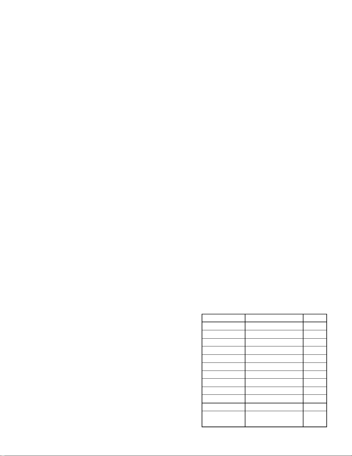
Tune to: Menu # For
1.9100 MHz F-24 [1.8 TX IF G] 75 W
3.7500 MHz F-25 [3.5 TX IF G] 75 W
7.0500 MHz F-26 [7 TX IF G] 75 W
10.1000 MHz F-27 [10 TX IF G] 75 W
14.2000 MHz F-28 [14 TX IF G] 75 W
18.1100 MHz F-29 [18 TX IF G] 75 W
21.2500 MHz F-30 [21 TX IF G] 75 W
24.9000 MHz F-31 [24 TX IF G] 75 W
28.8500 MHz F-32 [28 TX IF G] 75 W
52.0000 MHz F-33 [50 TX IF G] 75 W
145.5000 MHz F-35 [144 TX IF G] 40 W
435.0000 MHz
440.0000 MHz*
* TYP B1, B2, C1, C2
F-36 [430 TX IF G] 16 W
9
Alignment
ALC Meter Sensitivity
m Connect the 50-W dummy load and inline wattmeter to
the HF/50 MHz antenna jack. Connect the AF generator to the MIC jack.
m Tune the transceiver to 14.2000 MHz, select the USB
mode, and use Menu #21 to set the HF RF power to
maximum.
m Inject a 3.0 mV audio tone at 1 kHz to the MIC jack.
Then key the transmitter, and use Menu #25 adjust MIC
gain so the ALC meter just begun to deflect.
m Increase the injection level to 7.5 mV. Select “Align-
ment” menu item F-37 [ALC METER], and adjust the
main DIAL so that the ALC meter deflects to the top
edge of the ALC meter.
PO Meter Sensitivity
m Connect the 50-W dummy load and inline wattmeter to
the HF/50 MHz or VHF/UHF antenna jack, as appropriate for the steps below.
m Use Menu #21-24 to set the RF power for maximum on
the band being adjusted, and select the CW mode. Tune
the transceiver and select an “Alignment” menu item
per the chart below. Remember to move the dummy
load and inline wattmeter to the VHF/UHF antenna jack
for the last two steps.
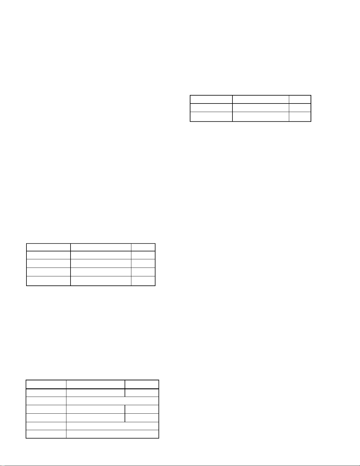
Tune to: Menu For
14.2000 MHz F-38 [HF PO METER] 10 dots
52.0000 MHz F-39 [50 PO METER] 10 dots
145.5000 MHz F-40 [144 PO METER] 6 dots
435.0000 MHz F-41 [430 PO METER] 4 dots
REV ALC Adjustment
m Connect the 16.6-W dummy load (or three 50-W loads
in parallel) to the HF/50 MHz antenna jack.
m Use Menu #21 and 22 to set the RF power for maxi-
mum on the band being adjusted below, and select the
CW mode. Tune the transceiver to each frequency
shown in the chart below and select the corresponding
“Alignment” menu item per the chart.
m Key the transmitter, and adjust the main DIAL for the
level shown in each step.
Tune to: Menu For
1.8400 MHz F-42 [HF REV ALC] 2 dots
for “Belgium” version only
14.2000 MHz ” 50 W
52.0000 MHz F-43 [50 REV ALC] 2 dots
for “France” version only
50 W
m Use Menu #23 and 24 to set the RF power for maxi-
mum on the band being adjusted below, and select the
CW mode. Tune the transceiver to the frequency shown
in the chart, and select an “Alignment” menu per the
chart (with no connection to the VHF/UHF antenna jack).
m Key the transmitter, and adjust the main DIAL for the
level shown in each step.
Tune to: Menu For
145.5000 MHz F-45 [144 REV ALC] 4 dots
435.0000 MHz F-46 [430 REV ALC] 3 dots
SWR Meter Adjustment
m Connect the 16.6-W dummy load (or three 50-W loads
in parallel) to the HF/50 MHz antenna jack.
m Set the transceiver to 3.7500 MHz, and use Menu #21 to
set the HF RF power for maximum. Select the CW mode.
Select “Alignment” menu item F-47 [SWR METER].
m Key the transmitter, and adjust the main DIAL for a
“3.0” indication on the transceiver’s SWR meter.
CW Carrier Level Adjustment
m Connect the 50-W dummy load to the HF/50 MHz an-
tenna jack.
m Set the transceiver to 1.5200 MHz and select the CW
mode. Select “Alignment” menu item F-50 [CW CAR
LEVEL].
m Key the transmitter, and adjust the main DIAL for a 2-
dot low from the full scale indication on the ALC meter.
AM Carrier Level Adjustment
m Leave the 50-W dummy load and inline wattmeter con-
nected to the HF/50 MHz antenna jack.
m Set the transceiver to 53.5000 MHz, and use Menu #22
to set the 50 MHz RF power for maximum. Use Menu
#25 to set the MIC gain for minimum. Select the AM
mode, and select “Alignment” menu item F-51 [AM
CAR LEVEL].
m Key the transmitter, and adjust the main DIAL for 6-
dot indication on the ALC meter.
FM Maximum Deviation
m With the 50 dB attenuator (or 50-W dummy load and
sampling coupler) and linear detector connected to the
HF/50 MHz antenna jack, connect the AF generator to
the MIC jack.
m Set the VR1002 to the 3 o'clock position, and enable the
CTCSS encoder at a frequency of 88.5Hz.
m
Set the transceiver to 29.2000 MHz, and select the FM mode.
m Key the transmitter, and adjust T1040 for ±0.8 kHz on
the deviation meter.
10

Alignment
m Inject a 10 mV audio signal at 1 kHz to the MIC jack,
and disable the CTCSS encoder.
m Key the transmitter, and adjust VR1002 for ±4.5 kHz
(±0.1 kHz) on the deviation meter.
m Now adjust VR1003 for ±2.3 kHz (±0.1 kHz) on the de-
viation meter.
FM TX LO Offset Adjustment m With the 50 dB attenuator (or 50-W dummy load and
sampling coupler) and frequency counter connected to
the HF/50 MHz antenna jack, connect the AF generator
to the MIC jack.
m Set the transceiver to 29.200 MHz, and select the FM-N
mode. Use Menu #26 to set the FM MIC gain to minimum. Select “Alignment” menu item F-52 [FM TX
FREQ].
m Key the transmitter, and adjust the main DIAL for
29.2000 MHz (±50 Hz) on the frequency counter.
TX and RX Carrier Point Adjustment
m With the 50-W dummy load and inline wattmeter con-
nected to the HF/50 MHz antenna jack, connect the AF
generator to the MIC jack.
m Set the transceiver to 14.2000 MHz, and select the LSB
mode. Select “Alignment” menu F-53 [TRX LSB CAR]
and preset it to “0” if it is not already set to that value.
m Key the transmitter, and adjust the AF generator’s fre-
quency for maximum indication on the inline wattme-
ter. Then adjust the AF generator’s level for 80 W on the
inline wattmeter.
m Set the AF generator’s frequency to 350 Hz.
m Key the transmitter, and adjust the main DIAL for 20
W (i.e. –6 dB from 80 W) on the inline wattmeter.
m Set the AF generator’s frequency to 2.1 kHz.
m Key the transmitter, and confirm at least 20 W on the
inline wattmeter.
m Leave the transceiver on 14.2000 MHz, and select the
USB mode. Select “Alignment” menu item F-54 [TRX
USB CAR], and preset it to “0” if it is not already set to
that value.
m Key the transmitter, and adjust the AF generator’s fre-
quency for maximum indication on the inline wattmeter. Then adjust the AF generator’s level for 80 W on
the inline wattmeter.
m Set the AF generator’s frequency to 350 Hz.
m Key the transmitter, and adjust the main DIAL for 20
W on the inline wattmeter.
m Set the AF generator’s frequency to 2.1 kHz.
m Key the transmitter, and confirm at least 20 W on the
inline wattmeter.
BEEP Level
m Set VR1004 for the position which provides the desired
“Beep” level.
11

Alignment
Note:
12
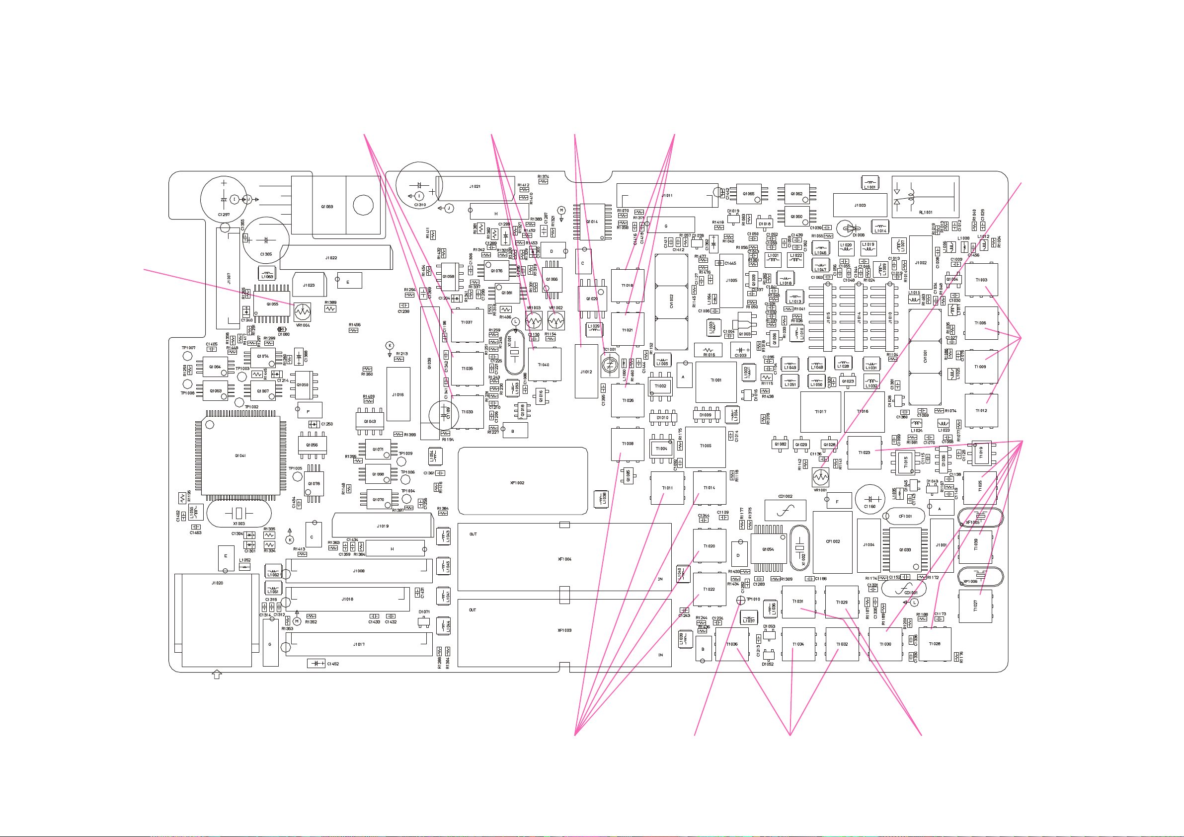
MAIN-Unit Alignment Points
Alignment
VR1004 BEEP Level
T1033, 35, 37
HF Band RX IF Sensitivity
HF/50 MHz Band RX IF Sensitivity
VR1002, 03
T1040
FM Maximum Deviation
TC1001
J1012
Trap Adjustment
T1018, 21, 26
144 MHz Band TX IF Transformer
VR1001
1st Mixer Balance
T1003, 06, 09, 12
144/430MHz Band RX IF Sensitivity
T1023, 25, 27, 28, 30, 39
HF Band RX IF Sensitivity
HF/50 MHz Band RX IF Sensitivity
T1008, 11, 14, 20, 22
HF/50 MHz Band TX IF Transformer
TP1010
Noise Blanker Alignment
: DC Voltmeter (Max)
T1032, 34, 36
HF Band RX IF Sensitivity
HF/50 MHz Band RX IF
Sensitivity
T1029, 31
Noise Blanker Alignment
13
Alignment
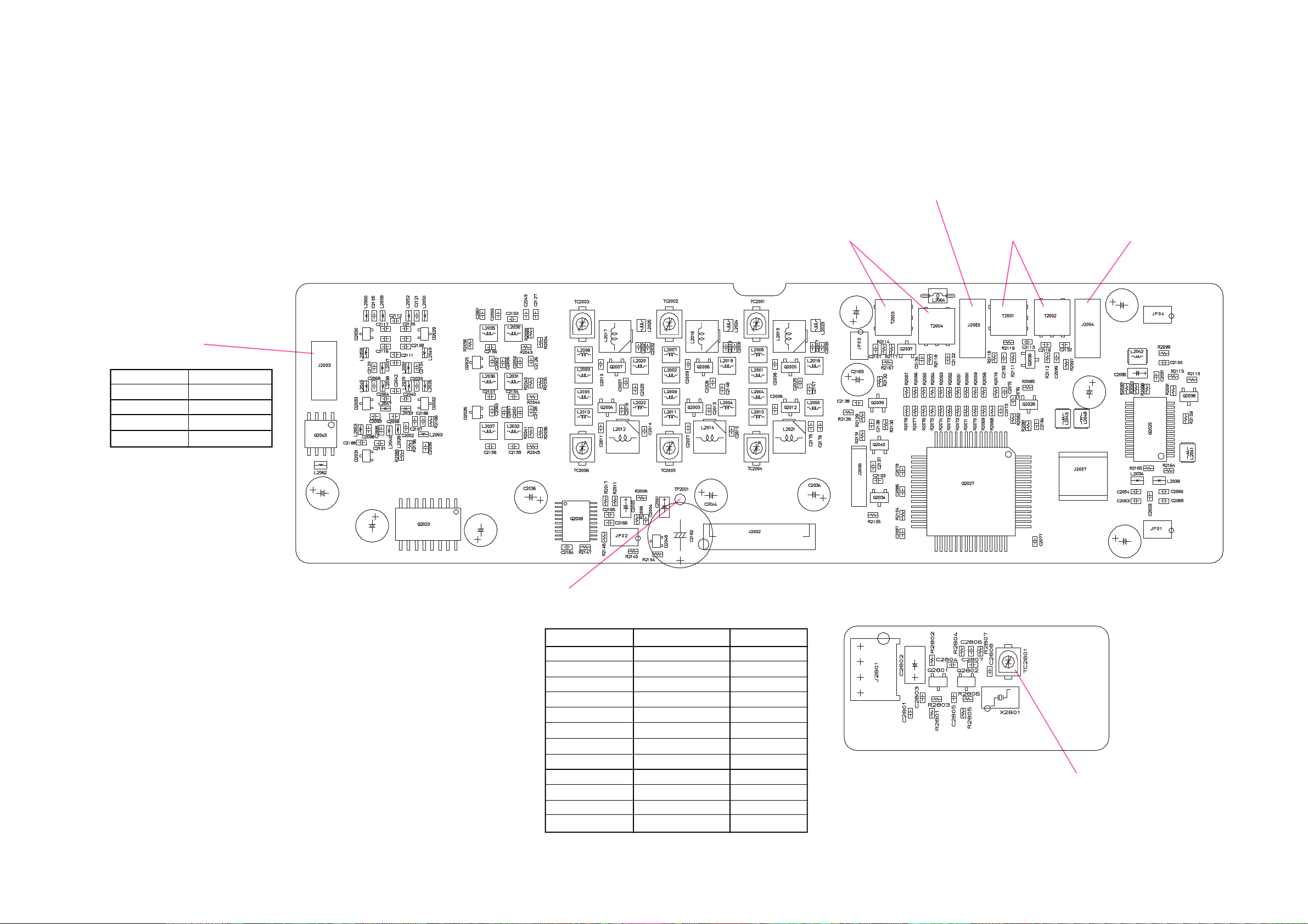
Local-Unit Alignment Points
J2005
Reference Frequency Adjust
: Frequency Counter (57.279999 MHz ± 60 Hz)
2nd Local Adjust
: RF Millivoltmeter (Max)
J2003
1st Local Output Level
: RF Millivoltmeter
Tune to: For
14.175 MHz 11 dBm ±3 dB
52.050 MHz 11 dBm ±3 dB
146.500 MHz 11 dBm ±3 dB
440.500 MHz 11 dBm ±3 dB
T2003, 04
2nd Local Adjust
T2001, 02
3rd Local Adjust
J2004
3rd Local Adjust
: RF Millivoltmeter (Max)
14
TP2001
VCO VCV Adjust
: DC Voltmeter
Tune to: Adjust/Confirm For
449.99999 MHz Adjust TC2005 7.4 V ± 0.1 V
420.00000 MHz Confirm 2.0 V ~ 4.8 V
381.99999 MHz Adjust TC2006 7.4 V ± 0.1 V
108.00000 MHz Confirm 1.2 V ~ 4.0 V
245.99999 MHz Adjust TC2004 7.4 V ± 0.1 V
60.00000 MHz Confirm 0.8 V ~ 4.0 V
197.99999 MHz Adjust TC2003 7.4 V ± 0.1 V
33.00000 MHz Confirm 1.2 V ~ 4.0 V
170.99999 MHz Adjust TC2002 7.4 V ± 0.1 V
15.00000 MHz Confirm 1.4 V ~ 4.2 V
14.99999 MHz Adjust TC2001 7.4 V ± 0.1 V
0.03000 MHz Confirm 1.5 V ~ 4.0 V
TC2801
Reference Frequency Adjust
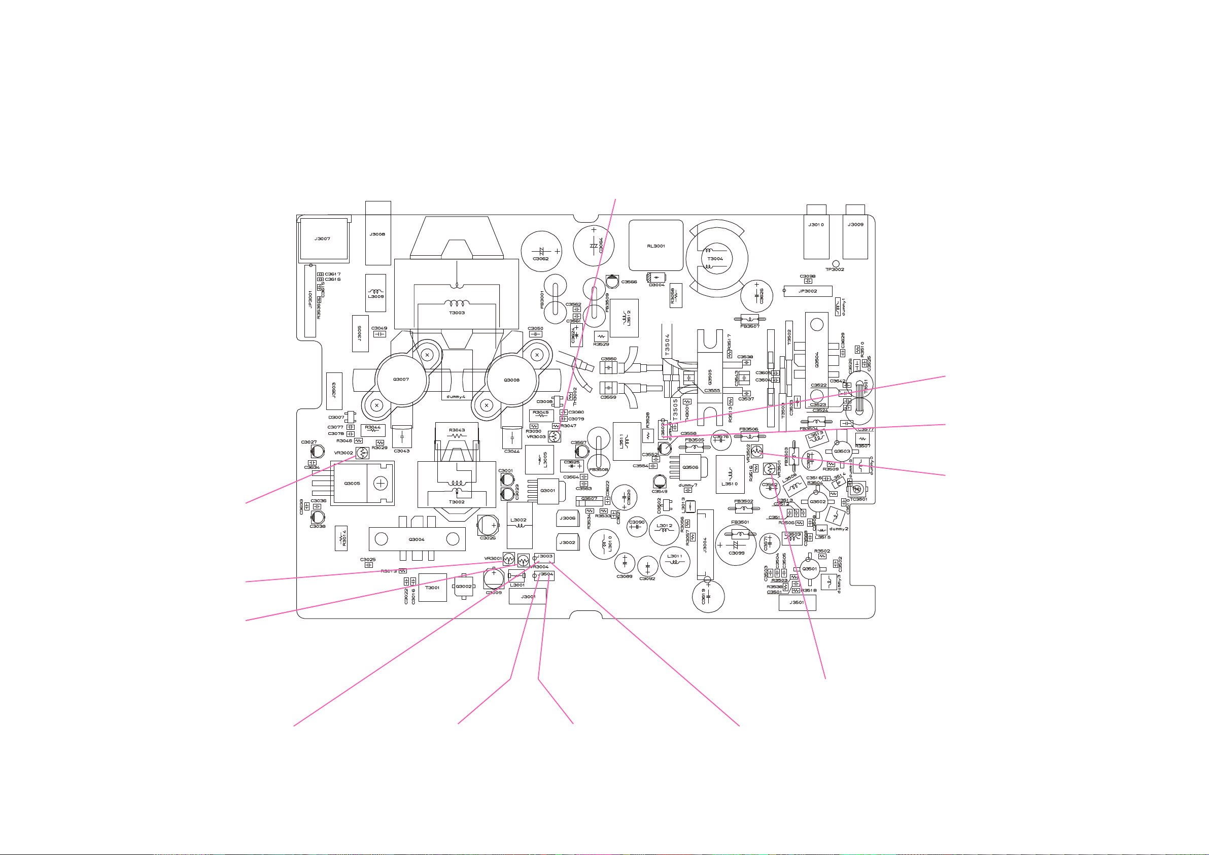
PA-Unit Alignment Points
Alignment
VR3003
HF/50 MHz Final Idling Current Adjust
VR3002
HF/50 MHz Final Idling Current Adjust
VR3001
HF/50 MHz Driver Section Idling Current
VR3004
HF/50 MHz Driver Section Idling Current
J3502 Pin-1
VHF/UHF Driver Section Idling Current
: Ammeter "-" lead (1.55A ± 50mA)
J3502 Pin-2
VHF/UHF Driver Section Idling Current
: Ammeter "+" lead (1.55A ± 50mA)
VR3502
VHF/UHF Final Idling Current Adjust
J3003 Pin-1
HF/50 MHz Driver Section Idling Current
: Ammeter "-" lead (1.1 A ± 50 mA)
J3504 Pin-1
HF/50 MHz Driver Section Idling Current
: Ammeter "-" lead (50 ~ 55 mA)
J3504 Pin-2
HF/50 MHz Driver Section Idling Current
: Ammeter "+" lead (50 ~ 55 mA)
VR3501
VHF/UHF Driver Section Idling Current
J3003 Pin-2
HF/50 MHz Driver Section Idling Current
: Ammeter "+" lead (1.1 A ± 50 mA)
15
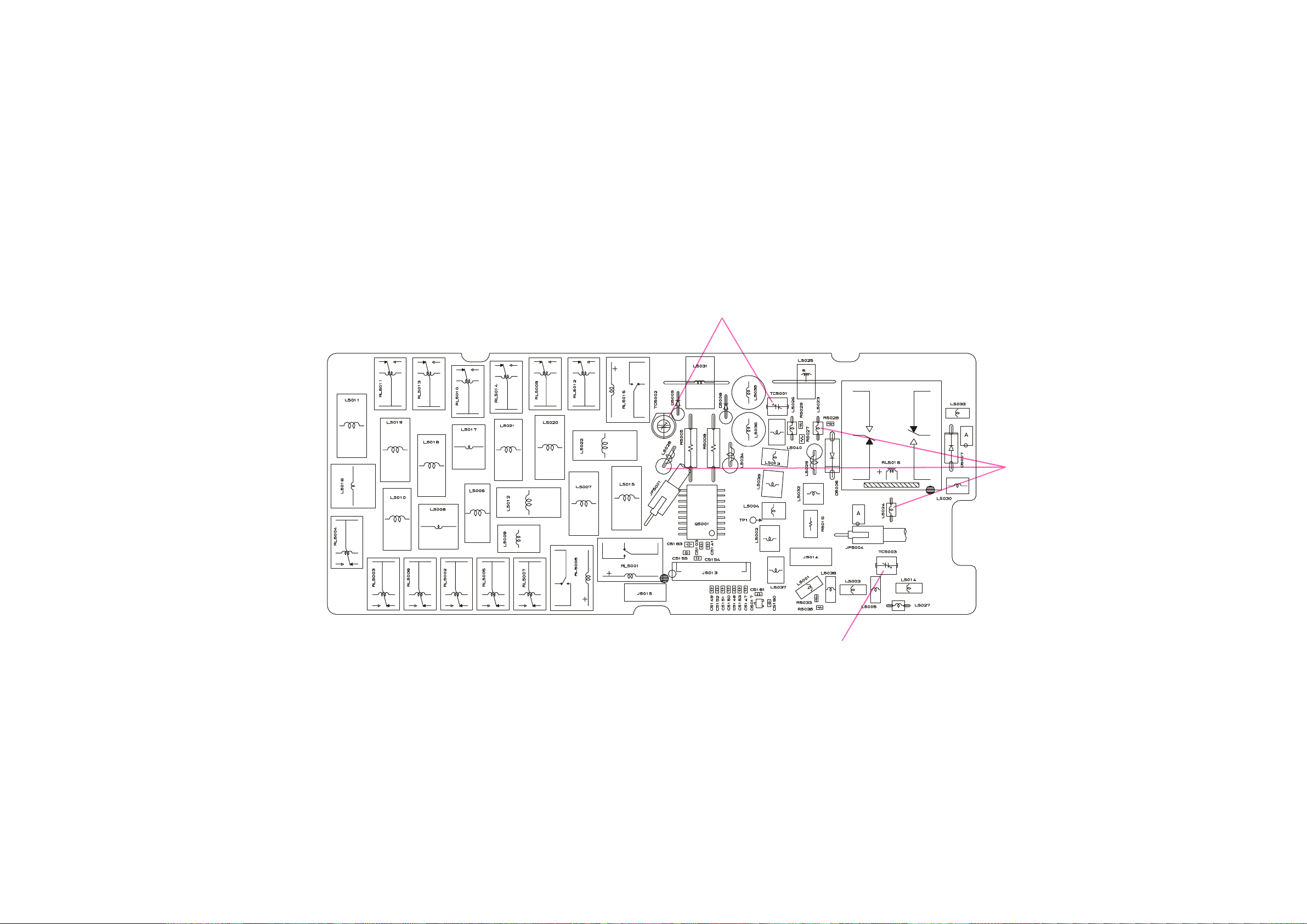
Alignment
LPF-Unit Alignment Points
TC5001, 02
CM Coupler Balance
TC5003
CM Coupler Balance
L5023, 24, 28
CM Coupler Balance
:DC Voltmeter (0V)
16
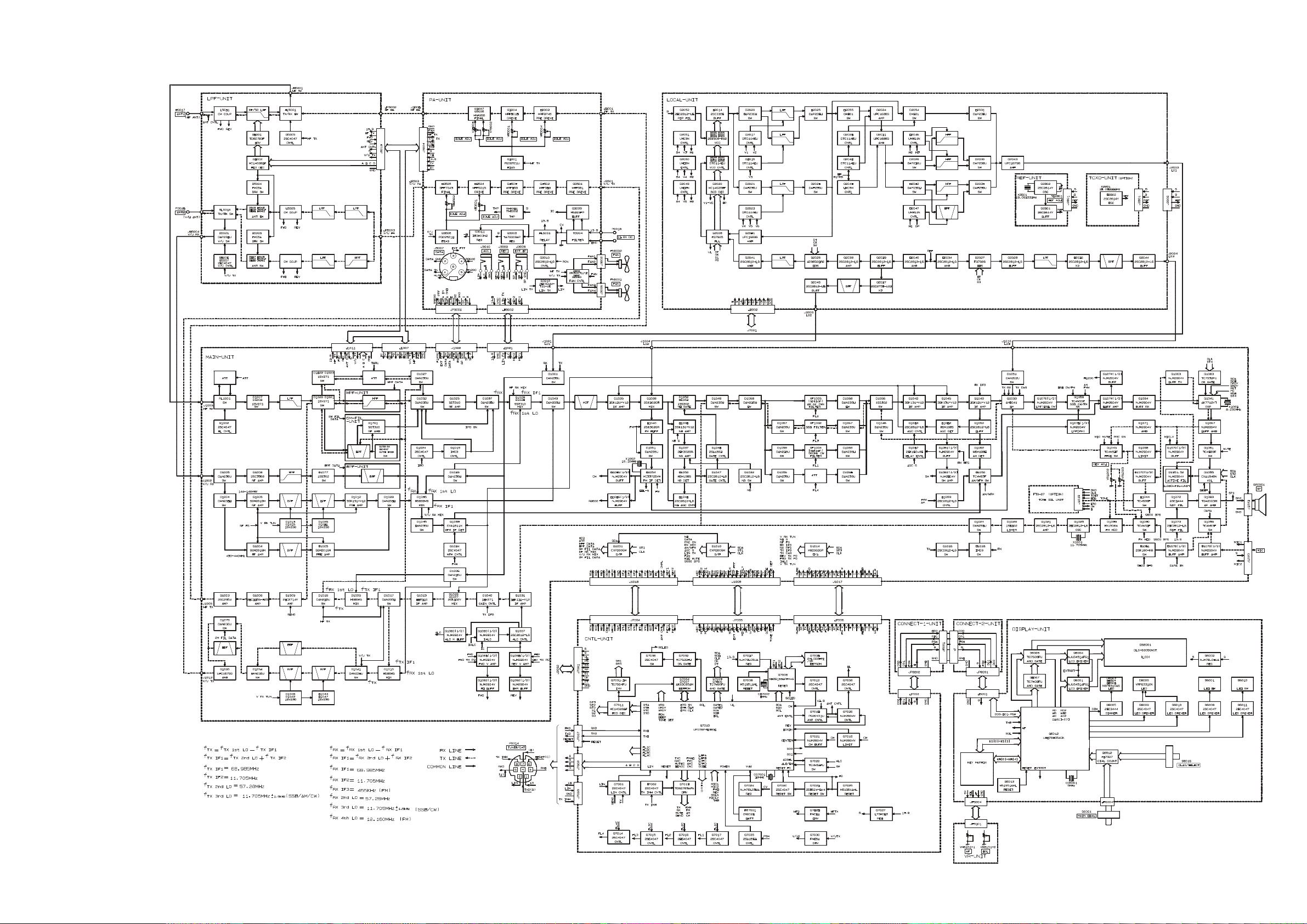
Block Diagram
17
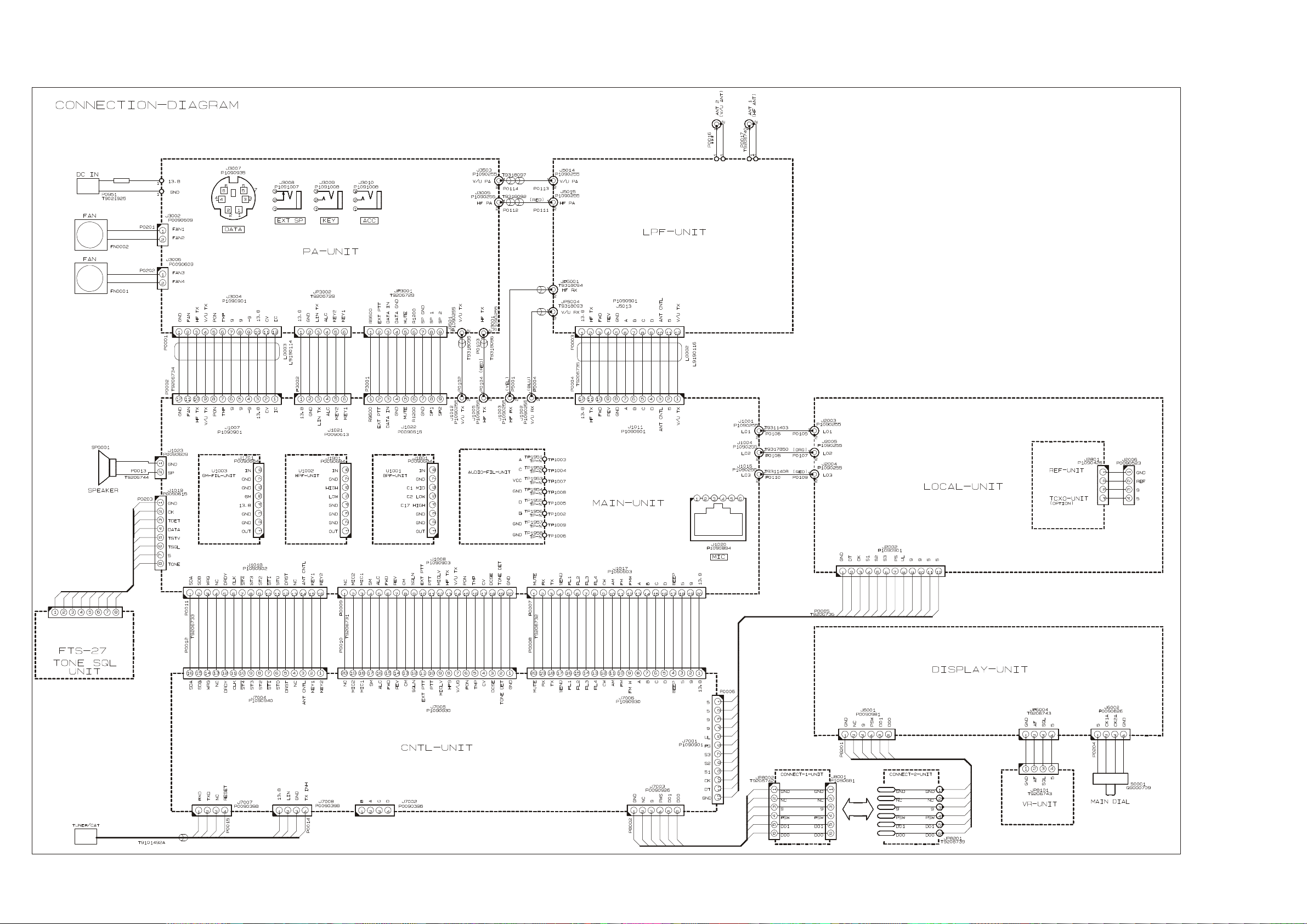
Interconnection Diagram
18
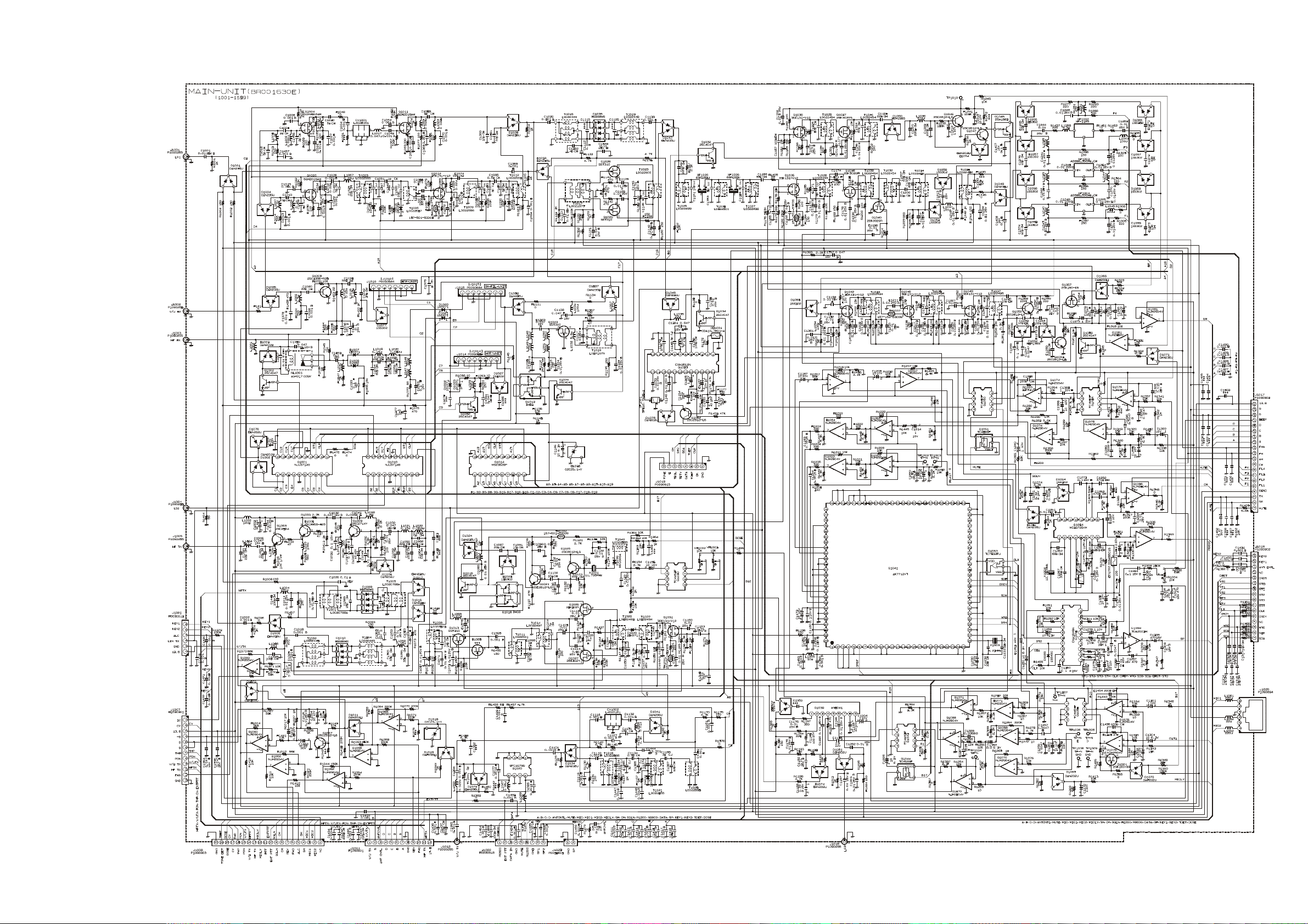
Circuit Diagram
MAIN Unit (Lot. 1~4)
19

MAIN Unit (Lot. 1~4)
Note:
20
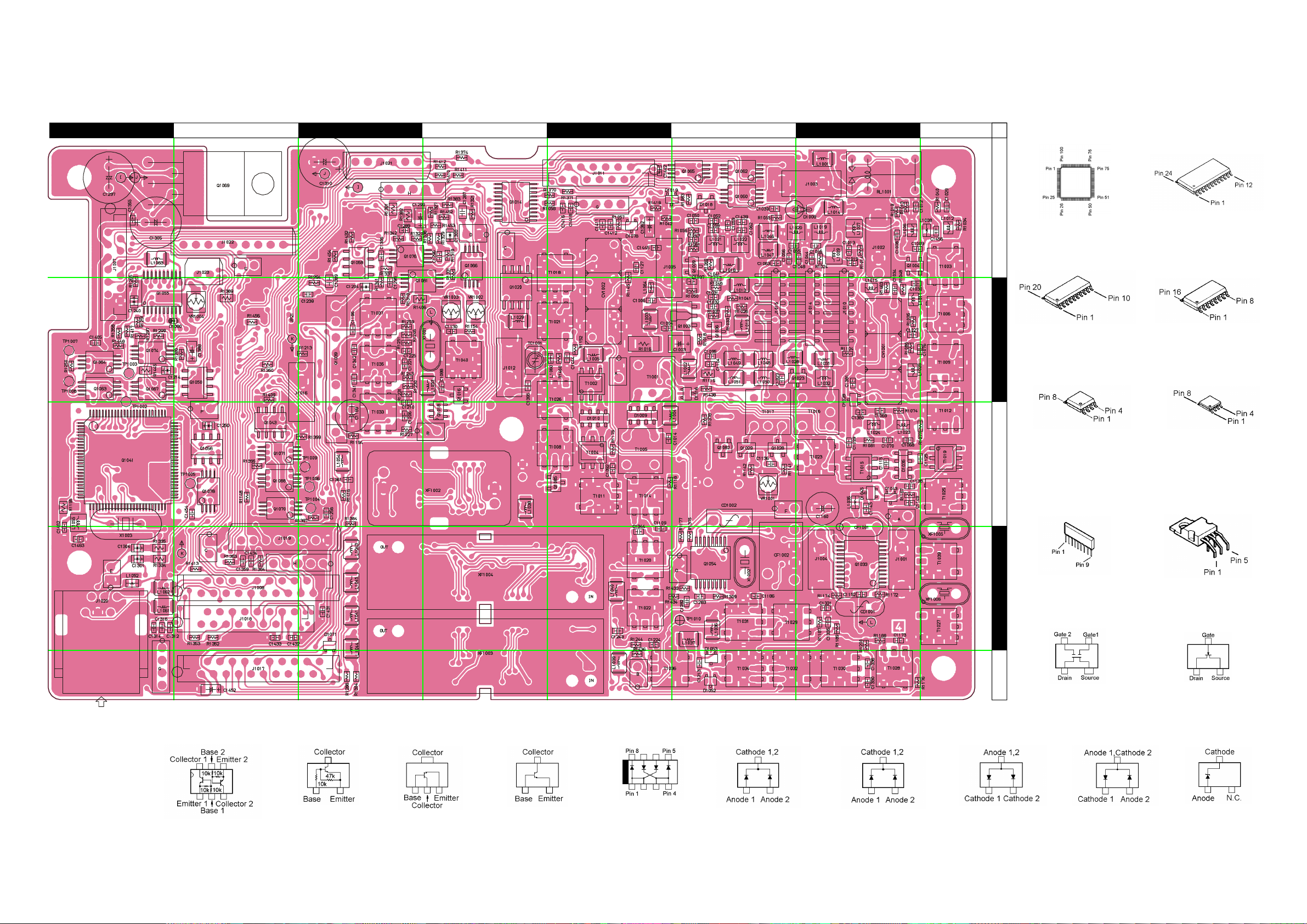
Parts Layout
MAIN Unit (Lot. 1~4)
A C D
B E
F H
G
1
AK7712VT
(Q1041)
2
3
M62352GP
(Q1014)
CXA1846N
(Q1055)
NJM2904V
(Q1060, 1062, 1063,
1064, 1065, 1066,
1067, 1068, 1070,
1071, 1074, 1076,
1078, 1081)
µPC1679G
(Q1020)
CXA1611N
(Q1033)
MC3372SVMEL
(Q1054)
TC4W53F
(Q 1043, 1050, 1056,
1058)
IMD3 (D3)
(Q1018)
2SC4047 (ZY)
(Q1016, 1082)
2SC2954 (QK)
(Q1003)
2SC2714Y (QY)
(Q1009)
2SC3356 (R25)
(Q1006)
HSB88WSTR
(D1009, 1010, 1035)
DAN202U (N)
(D1078)
DAN235U (M)
(D1016, 1028, 1043,
1045, 1071)
Side A
4
5
DAP202U (P)
(D1019)
AN6041
(Q1039)
SGM2016M (M-)
(Q1004)
1SS302 (C3)
(D1052, 1053)
TDA2003H
(Q1069)
SST310 (Z0)
(Q1023, 1028, 1029)
02CZ5.1Y (5.1)
(D1018)
21

MAIN Unit (Lot. 1~4)
a c d f hb e g
1
CXP2005M (Lot. 1)
NJU3714G (Lot. 2~)
(Q1001, 1010)
2
3
TC4S66F (C9)
(Q1044, 1051)
2SK160 (K6)
(Q1057, 1061)
SST310 (Z0)
(Q1013)
3SK131 (V12)
(Q1012, 1031, 1035, 1036,
SGM2016M (M-)
(Q1005, 1011)
TC4W53F
(Q1030)
TC7S32FU (E4)
(Q1083)
1042, 1045, 1049)
22
2SC3444 (DE)
(Q1072)
2SC2812 (L6)
(Q1007, 1021, 1025,
1046, 1047, 1052,
1053, 1073, 1084)
2SC3356 (R25)
(Q1008)
DAN202U (N)
(D1002, 1003, 1011, 1048, 1051, 1054,
1063, 1070, 1072, 1074, 1075, 1076)
DAN235U (M)
(D1001, 1004, 1005, 1006, 1017, 1024,
1032, 1033, 1034, 1037, 1041, 1046,
1061, 1079)
1SS302 (C3)
(D1027, 1029, 1055,
1056, 1057, 1058,
1059, 1064, 1066,
1067, 1068, 1069,
1073, 1077)
Side B
4
5
HSM198S (C6)
(D1050, 1060, 1062)
IMD3 (D3)
(Q1019)
2SC4047 (ZY)
(Q1002, 1024, 1032,
1034, 1059)
DAP202U (P)
(D1065)
2SK302GR (TG)
(Q1037, 1038, 1040)
2SK302Y (TY)
(Q1026, 1027)
2SA1563B (RL)
(Q1048)
02CZ5.1Y (5.1)
(D1036)
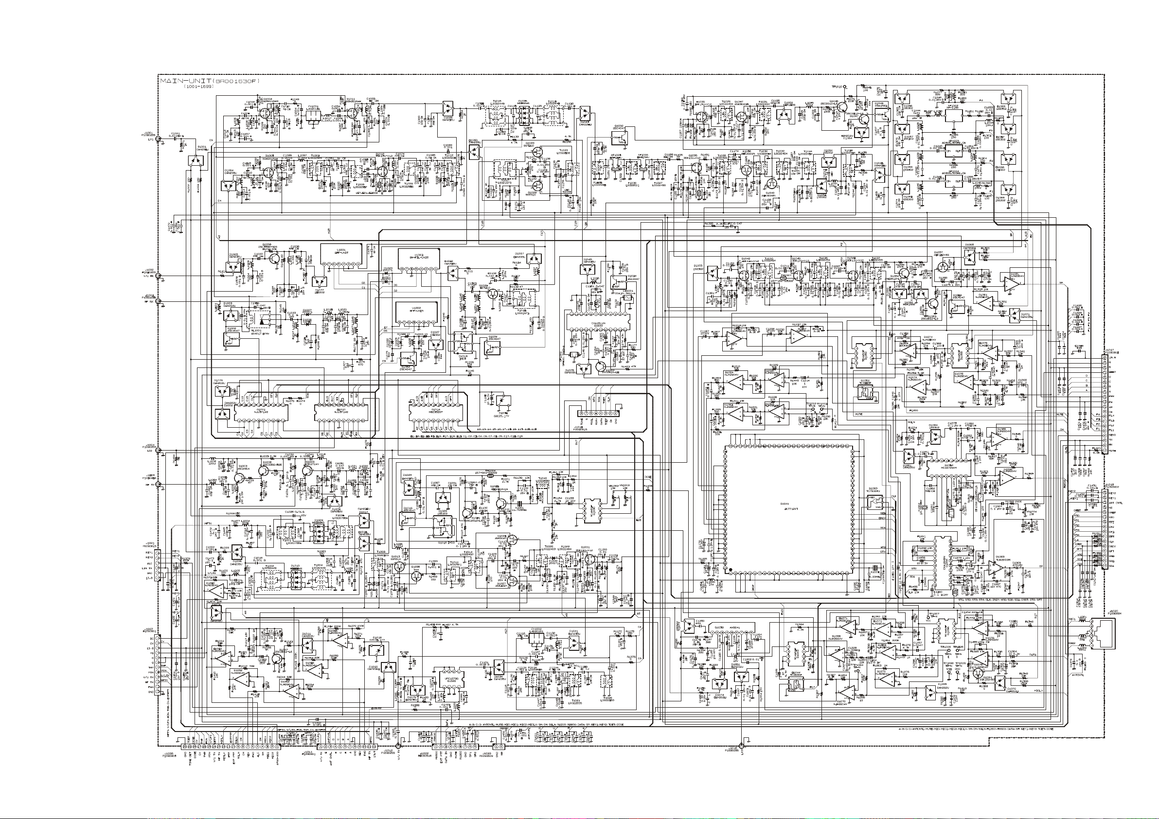
Circuit Diagram
MAIN Unit (Lot. 5~)
23

MAIN Unit (Lot. 5~)
Note:25Parts Layout
24

MAIN Unit (Lot. 5~)
A C D
B E
F H
G
1
AK7712VT
(Q1041)
2
3
M62352GP
(Q1014)
CXA1846N
(Q1055)
NJM2904V
(Q1060, 1062, 1063,
1064, 1065, 1066,
1067, 1068, 1070,
1071, 1074, 1076,
1078, 1081)
µPC1679G
(Q1020)
CXA1611N
(Q1033)
MC3372SVMEL
(Q1054)
TC4W53F
(Q 1043, 1050, 1056,
1058)
IMD3 (D3)
(Q1018)
2SC4047 (ZY)
(Q1016, 1082)
2SC2954 (QK)
(Q1003)
2SC2714Y (QY)
(Q1009)
2SC3356 (R25)
(Q1006)
HSB88WSTR
(D1009, 1010, 1035)
DAN202U (N)
(D1078)
DAN235U (M)
(D1016, 1028, 1043,
1045, 1071)
Side A
4
5
DAP202U (P)
(D1019)
AN6041
(Q1039)
SGM2016M (M-) (Lot. 1~4)
SGM2016AM (MA) (Lot. 5~)
(Q1004)
1SS302 (C3)
(D1052, 1053)
TDA2003H
(Q1069)
SST310 (Z0)
(Q1023, 1028, 1029)
02CZ5.1Y (5.1)
(D1018)
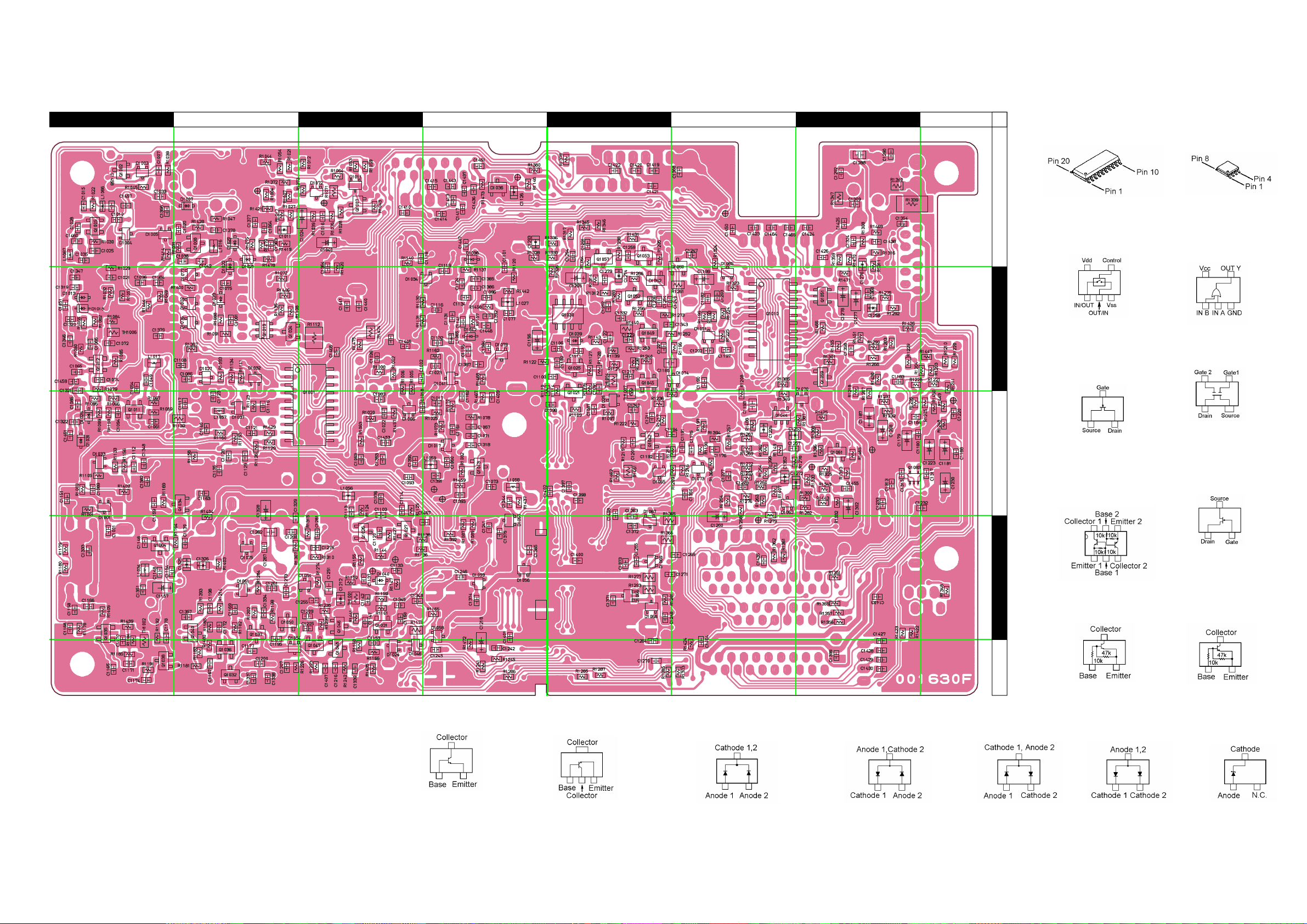
MAIN Unit (Lot. 5~)
a c d f hb e g
1
CXP2005M (Lot. 1)
NJU3714G (Lot. 2~)
(Q1001, 1010)
2
3
TC4S66F (C9)
(Q1044, 1051)
2SK160 (K6)
(Q1057, 1061)
SST310 (Z0)
(Q1013)
3SK131 (V12)
(Q1012, 1031, 1035, 1036,
SGM2016M (M-) (Lot. 1~4)
SGM2016AM (MA) (Lot. 5~)
(Q1005, 1011)
TC4W53F
(Q1030)
TC7S32FU (E4)
(Q1083)
1042, 1045, 1049)
26
2SC2812 (L6) (Lot. 1~18)
2SC2812NL6 (Lot. 19~)
(Q1007, 1021, 1025, 1046,
1047, 1052, 1053, 1084)
2SC2812 (L6)
(Q1073)
2SC3356 (R25)
(Q1008)
2SC3444 (DE)
(Q1072)
DAN202U (N)
(D1002, 1003, 1011, 1048, 1051, 1054,
1063, 1070, 1072, 1074, 1075, 1076)
DAN235U (M)
(D1001, 1004, 1005, 1006, 1017, 1024,
1032, 1033, 1034, 1037, 1041, 1046,
1061, 1079)
1SS302 (C3)
(D1027, 1029, 1055,
1056, 1057, 1058,
1059, 1064, 1066,
1067, 1068, 1069,
1073, 1077)
Side B
4
5
HSM198S (C6)
(D1050, 1060, 1062)
IMD3 (D3)
(Q1019)
2SC4047 (ZY)
(Q1002, 1024, 1032,
1034, 1059)
DAP202U (P)
(D1065)
2SK302GR (TG)
(Q1037, 1038, 1040)
2SK302Y (TY)
(Q1026, 1027)
2SA1563B (RL)
(Q1048)
02CZ5.1Y (5.1)
(D1036)
MAIN Unit
Parts List
DESCRIPTION VALUE V/W VXSTD P/NMFR’S DESIG VERS.REF. LOT. SIDE LAY ADR
*** MAIN-UNIT ***
PCB with Components CP6070003
PCB with Components (w/ XF-117C) CP6070006
PCB with Components (w/ XF-117C, XF-117CN) CP6070008
Printed Circuit Board FR001630E
C 1001 CHIP CAP. 0.01uF 25V B GRM39B103K25PT K22144803 1- B a4
C 1002 CHIP CAP. 0.001uF 50V B GRM39B102K50PT K22174821 1- B c2
C 1003 CHIP TA.CAP. 10uF 16V TEMSVB21C106M-8R K78120025 1- A F2
C 1004 CHIP CAP. 0.01uF 25V B GRM39B103K25PT K22144803 1- A E2
C 1005 CHIP CAP. 0.001uF 50V B GRM39B102K50PT K22174821 1
C 1006 CHIP CAP. 0.047uF 16V B GRM39B473K16PT K22124804 1- A E2
C 1007 CHIP CAP. 0.01uF 25V B GRM39B103K25PT K22144803 1- B a1
C 1008 CHIP CAP. 0.001uF 50V B GRM39B102K50PT K22174821 1- A G1
C 1009 CHIP CAP. 0.001uF 50V B GRM39B102K50PT K22174821 1 A G1
C 1009 CHIP CAP. 2pF 50V CK GRM39CK020C50PT K22174203 2- A G1
C 1010 CHIP CAP. 0.001uF 50V B GRM39B102K50PT K22174821 1 B a1
C 1010 CHIP CAP. 5pF 50V CH GRM39CH050C50PT K22174206 2- B a1
C 1011 CHIP TA.CAP. 0.68uF 10V TESVSP1A684M-8R K78100025 1- B b1
C 1012 CHIP CAP. 0.001uF 50V B GRM39B102K50PT K22174821 1 A G1
C 1012 CHIP CAP. 5pF 50V CH GRM39CH050C50PT K22174206 2- A G1
C 1013 CHIP CAP. 0.001uF 50V B GRM39B102K50PT K22174821 1- A G1
C 1014 CHIP CAP. 0.01uF 25V B GRM39B103K25PT K22144803 1- A E3
C 1015 CHIP CAP. 0.001uF 50V B GRM39B102K50PT K22174821 1- B a1
C 1016 CHIP CAP. 0.01uF 25V B GRM39B103K25PT K22144803 1- B c1
C 1017 CHIP CAP. 0.001uF 50V B GRM39B102K50PT K22174821 1- B d3
C 1018 CHIP CAP. 0.001uF 50V B GRM39B102K50PT K22174821 1- B c3
C 1019 CHIP CAP. 0.001uF 50V B GRM39B102K50PT K22174821 1- A G1
C 1020 CHIP CAP. 100pF 50V CH GRM39CH101J50PT K22174235 1 B b1
C 1020 CHIP CAP. 22pF 50V CH GRM39CH220J50PT K22174219 2- B b1
C 1021 CHIP CAP. 0.001uF 50V B GRM39B102K50PT K22174821 1- B a2
C 1022 CHIP CAP. 0.01uF 25V B GRM39B103K25PT K22144803 1- B c3
C 1023 CHIP CAP. 0.001uF 50V B GRM39B102K50PT K22174821 1- B d2
C 1024 CHIP TA.CAP. 10uF 10V TEMSVA1A106M-8R K78100028 1- B c1
C 1025 CHIP CAP. 0.001uF 50V B GRM39B102K50PT K22174821 1- B a1
C 1026 CHIP CAP. 0.01uF 25V B GRM39B103K25PT K22144803 1- B c2
C 1027 CHIP CAP. 0.001uF 50V B GRM39B102K50PT K22174821 1- A G2
C 1028 CHIP CAP. 5pF 50V CH GRM39CH050C50PT K22174206 1 B a1
C 1028 CHIP CAP. 0.001uF 50V B GRM39B102K50PT K22174821 2- B a1
C 1029 CHIP CAP. 0.001uF 50V B GRM39B102K50PT K22174821 1- A H1
C 1030 CHIP CAP. 3pF 50V CJ GRM39CJ030C50PT K22174204 1 A G2
C 1030 CHIP CAP. 5pF 50V CH GRM39CH050C50PT K22174206 2- A G2
C 1031 CHIP CAP. 0.01uF 25V B GRM39B103K25PT K22144803 1 A F2
C 1031 CHIP CAP. 0.1uF 16V B GRM39B104K16PT K22124805 2- A F2
C 1032 CHIP CAP. 0.047uF 16V B GRM39B473K16PT K22124804 1- A F2
C 1033 CHIP CAP. 0.1uF 16V B GRM39B104K16PT K22124805 1- B a1
C 1034 CHIP CAP. 0.001uF 50V B GRM39B102K50PT K22174821 1- A G2
C 1035 CHIP CAP. 1pF 50V CK GRM39CK010C50PT K22174202 1 B a1
C 1035 CHIP CAP. 22pF 50V CH GRM39CH220J50PT K22174219 2- B a1
C 1036 CHIP CAP. 0.001uF 50V B GRM39B102K50PT K22174821 1- B a2
C 1037 CHIP CAP. 0.01uF 25V B GRM39B103K25PT K22144803 1- A F2
C 1038 CHIP CAP. 2pF 50V CK GRM39CK020C50PT K22174203 1 B b1
C 1038 CHIP CAP. 33pF 50V CH GRM39CH330J50PT K22174223 2- B b1
C 1039 CHIP CAP. 0.1uF 16V B GRM39B104K16PT K22124805 1- A F1
C 1040 CHIP TA.CAP. 10uF 10V TEMSVA1A106M-8R K78100028 1- B c1
C 1041 CHIP CAP. 0.0068uF 50V B GRM39B682M50PT K22174819 1- A F2
C 1042 CHIP CAP. 2pF 50V CK GRM39CK020C50PT K22174203 1 B b1
C 1042 CHIP CAP. 33pF 50V CH GRM39CH330J50PT K22174223 2- B b1
C 1043 CHIP CAP. 0.01uF 25V B GRM39B103K25PT K22144803 1- A F1
C 1044 CHIP CAP. 47pF 50V CH GRM39CH470J50PT K22174227 1 A G1
C 1044 CHIP CAP. 82pF 50V CH GRM39CH820J50PT K22174233 2- A G1
C 1046 CHIP CAP. 15pF 50V CH GRM39CH150J50PT K22174215 1 A G1
C 1046 CHIP CAP. 22pF 50V CH GRM39CH220J50PT K22174219 2- A G1
C 1048 CHIP CAP. 82pF 50V CH GRM39CH820J50PT K22174233 1 A G1
C 1048 CHIP CAP. 100pF 50V CH GRM39CH101J50PT K22174235 2- A G1
C 1049 CHIP CAP. 0.001uF 50V B GRM39B102K50PT K22174821 1- B a2
C 1050 CHIP CAP. 0.047uF 16V B GRM39B473K16PT K22124804 1- A F1
C 1051 CHIP CAP. 0.5pF 50V CK GRM39CK0R5C50PT K22174201 1 B a2
Printed Circuit Board FR001630F 5-
27
MAIN Unit
DESCRIPTION VALUE V/W TOL. VXSTD P/NMFR’S DESIG VERS.REF. LOT. SIDE LAY ADR
C 1051 CHIP CAP. 1pF 50V CK GRM39CK010C50PT K22174202 2- B a2
C 1052 CHIP CAP. 33pF 50V CH GRM39CH330J50PT K22174223 1 A F1
C 1052 CHIP CAP. 82pF 50V CH GRM39CH820J50PT K22174233 2- A F1
C 1053 CHIP CAP. 0.01uF 25V B GRM39B103K25PT K22144803 1- B c3
C 1054 CHIP CAP. 0.001uF 50V B GRM39B102K50PT K22174821 1- B a2
C 1055 CHIP CAP. 56pF 50V CH GRM39CH560J50PT K22174229 1 A F1
C 1055 CHIP CAP. 68pF 50V CH GRM39CH680J50PT K22174231 2- A F1
C 1056 CHIP CAP. 33pF 50V CH GRM39CH330J50PT K22174223 1 A F1
C 1056 CHIP CAP. 56pF 50V CH GRM39CH560J50PT K22174229 2- A F1
C 1058 CHIP CAP. 56pF 50V CH GRM39CH560J50PT K22174229 1 A F1
C 1058 CHIP CAP. 22pF 50V CH GRM39CH220J50PT K22174219 2- A F1
C 1059 CHIP CAP. 82pF 50V CH GRM39CH820J50PT K22174233 1 A F1
C 1059 CHIP CAP. 100pF 50V CH GRM39CH101J50PT K22174235 2- A F1
C 1060 CHIP CAP. 0.001uF 50V B GRM39B102K50PT K22174821 1- B d3
C 1061 CHIP CAP. 0.001uF 50V B GRM39B102K50PT K22174821 1- B a3
C 1062 CHIP CAP. 15pF 50V CH GRM39CH150J50PT K22174215 1 A F1
C 1062 CHIP CAP. 68pF 50V CH GRM39CH680J50PT K22174231 2- A F1
C 1063 CHIP CAP. 0.1uF 16V B GRM39B104K16PT K22124805 1- A F1
C 1064 CHIP CAP. 47pF 50V CH GRM39CH470J50PT K22174227 1 B b1
C 1064 CHIP CAP. 56pF 50V CH GRM39CH560J50PT K22174229 2- B b1
C 1065 CHIP CAP. 0.001uF 50V B GRM39B102K50PT K22174821 1- B a2
C 1066 CHIP CAP. 0.001uF 50V B GRM39B102K50PT K22174821 1 B a2
C 1066 CHIP CAP. 22pF 50V CH GRM39CH220J50PT K22174219 2- B a2
C 1067 CHIP CAP. 0.01uF 25V B GRM39B103K25PT K22144803 1- B d3
C 1068 CHIP CAP. 0.001uF 50V B GRM39B102K50PT K22174821 1- A G3
C 1069 CHIP CAP. 10pF 50V CH GRM39CH100D50PT K22174211 1 A G3
C 1069 CHIP CAP. 6pF 50V CH GRM39CH060D50PT K22174207 2- A G3
C 1070 CHIP CAP. 0.001uF 50V B GRM39B102K50PT K22174821 1- A G3
C 1071 CHIP CAP. 0.01uF 25V B GRM39B103K25PT K22144803 1- B d3
C 1072 CHIP CAP. 0.001uF 50V B GRM39B102K50PT K22174821 1- B a2
C 1073 CHIP CAP. 0.01uF 25V B GRM39B103K25PT K22144803 1- B d3
C 1074 CHIP CAP. 3pF 50V CJ GRM39CJ030C50PT K22174204 1 B a2
C 1074 CHIP CAP. 22pF 50V CH GRM39CH220J50PT K22174219 2- B a2
C 1076 CHIP CAP. 0.001uF 50V B GRM39B102K50PT K22174821 1- A H2
C 1077 CHIP CAP. 0.0018uF 50V B GRM39B182M50PT K22174812 1- B d2
C 1079 CHIP CAP. 5pF 50V CH GRM39CH050C50PT K22174206 1
C 1080 CHIP CAP. 0.01uF 25V B GRM39B103K25PT K22144803 1
C 1081 CHIP CAP. 0.047uF 16V B GRM39B473K16PT K22124804 1- B b2
C 1084 CHIP CAP. 0.001uF 50V B GRM39B102K50PT K22174821 1
C 1085 CHIP CAP. 0.5pF 50V CK GRM39CK0R5C50PT K22174201 1 B a3
C 1085 CHIP CAP. 0.5pF 50V CK GRM39CK0R5C50PT K22174201 2- B a3
C 1087 CHIP CAP. 10pF 50V CH GRM39CH100C50PT K22174248 1 B e3
C 1087 CHIP CAP. 22pF 50V CH GRM39CH220J50PT K22174219 2- B e3
C 1088 CHIP CAP. 0.01uF 25V B GRM39B103K25PT K22144803 1- A D2
C 1089 CHIP CAP. 0.001uF 50V B GRM39B102K50PT K22174821 1- B a3
C 1091 CHIP CAP. 10pF 50V CH GRM39CH100C50PT K22174248 1- B e2
C 1092 CHIP CAP. 5pF 50V CH GRM39CH050C50PT K22174206 1 A E3
C 1092 CHIP CAP. 7pF 50V CH GRM39CH070D50PT K22174208 2- A E3
C 1093 CHIP CAP. 5pF 50V CH GRM39CH050C50PT K22174206 1 B c3
C 1093 CHIP CAP. 1pF 50V CK GRM39CK010C50PT K22174202 2- B c3
C 1094 CHIP CAP. 0.001uF 50V B GRM39B102K50PT K22174821 1- B a3
C 1095 CHIP CAP. 0.01uF 25V B GRM39B103K25PT K22144803 1- A F2
C 1096 CHIP CAP. 0.0018uF 50V B GRM39B182M50PT K22174812 1- B d2
C 1098 CHIP CAP. 0.01uF 25V B GRM39B103K25PT K22144803 1- B e3
C 1099 CHIP CAP. 0.001uF 50V B GRM39B102K50PT K22174821 1- A G3
C 1100 CHIP CAP. 10pF 50V CH GRM39CH100C50PT K22174248 1- B e2
C 1101 CHIP CAP. 0.0018uF 50V B GRM39B182M50PT K22174812 1- B d2
C 1102 CHIP CAP. 0.01uF 25V B GRM39B103K25PT K22144803 1- B e2
C 1103 CHIP CAP. 15pF 50V CH GRM39CH150J50PT K22174215 1 B c4
C 1103 CHIP CAP. 7pF 50V CH GRM39CH070D50PT K22174208 2- B c4
C 1104 CHIP CAP. 0.01uF 25V B GRM39B103K25PT K22144803 1- A F2
C 1106 CHIP CAP. 100pF 50V CH GRM39CH101J50PT K22174235 1- B e2
C 1108 CHIP CAP. 0.047uF 16V B GRM39B473K16PT K22124804 1- B b2
C 1109 CHIP CAP. 0.01uF 25V B GRM39B103K25PT K22144803 1- A E4
C 1110 CHIP CAP. 0.01uF 25V B GRM39B103K25PT K22144803 1- B b3
C 1111 CHIP CAP. 180pF 50V CH GRM39CH181J50PT K22174241 1 B e2
C 1111 CHIP CAP. 22pF 50V CH GRM39CH220J50PT K22174219 2- B e2
C 1112 CHIP CAP. 0.001uF 50V B GRM39B102K50PT K22174821 1- B a3
28
MAIN Unit
REF.
C 1113 CHIP CAP. 0.01uF 25V B GRM39B103K25PT K22144803 1- B c3
C 1114 CHIP CAP. 0.01uF 25V B GRM39B103K25PT K22144803 1- B c3
C 1115 CHIP CAP. 1pF 50V CK GRM39CK010C50PT K22174202 1-1 A G3
C 1115 CHIP CAP. 10pF 50V CH GRM39CH100D50PT K22174211 3 A G3
C 1116 CHIP CAP. 0.001uF 50V B GRM39B102K50PT K22174821 1- B d2
C 1117 CHIP CAP. 0.01uF 25V B GRM39B103K25PT K22144803 1- B b3
C 1118 CHIP CAP. 0.001uF 50V B GRM39B102K50PT K22174821 1- B c1
C 1118 CHIP CAP. 33pF 50V CH GRM39CH330J50PT K22174223 4- B c1
C 1119 CHIP CAP. 0.001uF 50V B GRM39B102K50PT K22174821 1- B d2
C 1120 CHIP CAP. 0.01uF 25V B GRM39B103K25PT K22144803 1 B c4
C 1120 CHIP CAP. 0.1uF 16V B GRM39B104K16PT K22124805 2- B c4
C 1121 CHIP CAP. 0.01uF 25V B GRM39B103K25PT K22144803 1 B b3
C 1121 CHIP CAP. 0.047uF 16V B GRM39B473K16PT K22124804 2- B b3
C 1122 CHIP CAP. 0.01uF 25V B GRM39B103K25PT K22144803 1- B e2
C 1123 CHIP CAP. 0.01uF 25V B GRM39B103K25PT K22144803 1- B b3
C 1124 CHIP CAP. 47pF 50V CH GRM39CH470J50PT K22174227 1 B d2
C 1124 CHIP CAP. 22pF 50V UJ GRM39UJ220J50PT K22174316 2- B d2
C 1125 CHIP CAP. 1pF 50V CK GRM39CK010C50PT K22174202 1 A H3
C 1126 CHIP TA.CAP. 10uF 10V TEMSVA1A106M-8R K78100028 1 B d1
C 1126 CHIP TA.CAP. 10uF 6.3V TESVSP0J106M-8R K78080055 2- B d1
C 1127 CHIP CAP. 0.001uF 50V B GRM39B102K50PT K22174821 1- A E1
C 1128 CHIP CAP. 0.01uF 25V B GRM39B103K25PT K22144803 1- B b3
C 1129 CHIP CAP. 0.01uF 25V B GRM39B103K25PT K22144803 1- B b3
C 1130 CHIP CAP. 0.01uF 25V B GRM39B103K25PT K22144803 1- A D2
C 1131 CHIP CAP. 0.001uF 50V B GRM39B102K50PT K22174821 1 B d2
C 1131 CHIP CAP. 18pF 50V CH GRM39CH180J50PT K22174217 2- B d2
C 1132 CHIP CAP. 0.001uF 50V B GRM39B102K50PT K22174821 1- B d2
C 1133 CHIP CAP. 0.01uF 25V B GRM39B103K25PT K22144803 1- B c4
C 1134 CHIP CAP. 0.5pF 50V CK GRM39CK0R5C50PT K22174201 1 B d2
C 1134 CHIP CAP. 0.5pF 50V CK GRM39CK0R5C50PT K22174201 2- B d2
C 1135 CHIP CAP. 0.01uF 25V B GRM39B103K25PT K22144803 1- B b3
C 1136 CHIP CAP. 15pF 50V CH GRM39CH150J50PT K22174215 1 A F3
C 1136 CHIP CAP. 8pF 50V UJ GRM39UJ080D50PT K22174308 2- A F3
C 1137 CHIP CAP. 0.01uF 25V B GRM39B103K25PT K22144803 1- B c4
C 1138 CHIP CAP. 0.001uF 50V B GRM39B102K50PT K22174821 1- A G3
C 1139 CHIP CAP. 0.01uF 25V B GRM39B103K25PT K22144803 1- B b4
C 1140 CHIP CAP. 0.01uF 25V B GRM39B103K25PT K22144803 1- B b3
C 1141 CHIP CAP. 47pF 50V CH GRM39CH470J50PT K22174227 1 B d2
C 1141 CHIP CAP. 22pF 50V UJ GRM39UJ220J50PT K22174316 2- B d2
C 1142 CHIP CAP. 0.01uF 25V B GRM39B103K25PT K22144803 1- B c4
C 1143 CHIP CAP. 100pF 50V CH GRM39CH101J50PT K22174235 1- A G3
C 1144 CHIP CAP. 10pF 50V CH GRM39CH100D50PT K22174211 1
C 1145 CHIP CAP. 47pF 50V CH GRM39CH470J50PT K22174227 1
C 1146 CHIP CAP. 0.01uF 25V B GRM39B103K25PT K22144803 1- B a4
C 1147 CHIP CAP. 0.01uF 25V B GRM39B103K25PT K22144803 1- B c4
C 1148 CHIP CAP. 10pF 50V CH GRM39CH100D50PT K22174211 1 B a4
C 1148 CHIP CAP. 3pF 50V CJ GRM39CJ030C50PT K22174204 2 B a4
C 1148 CHIP CAP. 4pF 50V CH GRM39CH040C50PT K22174205 3- B a4
C 1149 CHIP CAP. 100pF 50V CH GRM39CH101J50PT K22174235 1 A G3
C 1149 CHIP CAP. 220pF 50V CH GRM39CH221J50PT K22174243 2- A G3
C 1150 CHIP CAP. 0.01uF 25V B GRM39B103K25PT K22144803 1- B c4
C 1151 CHIP CAP. 9pF 50V CH GRM39CH090D50PT K22174210 1 B a3
C 1151 CHIP CAP. 10pF 50V UJ GRM39UJ100D50PT K22174301 2- B a3
C 1152 CHIP CAP. 100pF 50V CH GRM39CH101J50PT K22174235 1- A G4
C 1153 CHIP CAP. 0.01uF 25V B GRM39B103K25PT K22144803 1- B c5
C 1154 CHIP CAP. 0.01uF 25V B GRM39B103K25PT K22144803 1- B a4
C 1155 CHIP CAP. 0.5pF 50V CK GRM39CK0R5C50PT K22174201 1 B d2
C 1155 CHIP CAP. 3pF 50V CJ GRM39CJ030C50PT K22174204 2- B d2
C 1156 CHIP TA.CAP. 10uF 10V TEMSVA1A106M-8R K78100028 1- B d2
C 1157 CHIP TA.CAP. 10uF 10V TEMSVA1A106M-8R K78100028 1- B a4
C 1158 CHIP CAP. 15pF 50V CH GRM39CH150J50PT K22174215 1 B a4
C 1158 CHIP CAP. 4pF 50V UJ GRM39UJ040C50PT K22174304 2- B a4
C 1159 CHIP CAP. 0.01uF 25V B GRM39B103K25PT K22144803 1- B a3
C 1160 AL.ELECTRO.CAP. 47uF 16V RE2-16V470M 47UF K40129054 1- A G3
C 1161 CHIP CAP. 0.001uF 50V B GRM39B102K50PT K22174821 1- B d3
C 1162 CHIP CAP. 0.001uF 50V B GRM39B102K50PT K22174821 1- B d3
C 1163 CHIP CAP. 0.01uF 25V B GRM39B103K25PT K22144803 1- B b3
C 1164 CHIP CAP. 47pF 50V CH GRM39CH470J50PT K22174227 1
DESCRIPTION VALUE V/W TOL. VXSTD P/NMFR’S DESIG VERS. LOT. SIDE LAY ADR
29
MAIN Unit
DESCRIPTION VALUE V/W TOL. VXSTD P/NMFR’S DESIG VERS.REF. LOT. SIDE LAY ADR
C 1165 CHIP CAP. 0.01uF 25V B GRM39B103K25PT K22144803 1- B a5
C 1165 CHIP CAP. 0.1uF 16V B GRM39B104K16PT K22124805 4- B a5
C 1166 CHIP CAP. 47pF 50V CH GRM39CH470J50PT K22174227 1 B a4
C 1166 CHIP CAP. 33pF 50V CH GRM39CH330J50PT K22174223 2- B a4
C 1167 CHIP CAP. 100pF 50V CH GRM39CH101J50PT K22174235 1- B b5
C 1168 CHIP CAP. 0.01uF 25V B GRM39B103K25PT K22144803 1- B a4
C 1169 CHIP CAP. 0.01uF 25V B GRM39B103K25PT K22144803 1- B b4
C 1170 CHIP CAP. 0.01uF 25V B GRM39B103K25PT K22144803 1- B a5
C 1171 CHIP CAP. 15pF 50V CH GRM39CH150J50PT K22174215 1 B a5
C 1171 CHIP CAP. 8pF 50V UJ GRM39UJ080D50PT K22174308 2- B a5
C 1172 CHIP CAP. 0.01uF 25V B GRM39B103K25PT K22144803 1- B b4
C 1173 CHIP CAP. 0.01uF 25V B GRM39B103K25PT K22144803 1- A G4
C 1174 CHIP CAP. 0.001uF 50V B GRM39B102K50PT K22174821 1- B a5
C 1175 CHIP CAP. 0.01uF 25V B GRM39B103K25PT K22144803 1- B f3
C 1176 CHIP CAP. 0.01uF 25V B GRM39B103K25PT K22144803 1- B f3
C 1177 CHIP CAP. 0.01uF 25V B GRM39B103K25PT K22144803 1- B b5
C 1178 CHIP CAP. 0.01uF 25V B GRM39B103K25PT K22144803 1- B a4
C 1179 CHIP TA.CAP. 10uF 10V TEMSVA1A106M-8R K78100028 1- B g3
C 1180 CHIP CAP. 0.1uF 16V B GRM39B104K16PT K22124805 1- B g3
C 1181 CHIP TA.CAP. 10uF 10V TEMSVA1A106M-8R K78100028 1- B h3
C 1182 CHIP CAP. 0.01uF 25V B GRM39B103K25PT K22144803 1- B f2
C 1183 CHIP CAP. 0.0015uF 50V B GRM39B152M50PT K22174811 1- B g2
C 1184 CHIP CAP. 0.0015uF 50V B GRM39B152M50PT K22174811 1- B g3
C 1185 CHIP TA.CAP. 10uF 10V TEMSVA1A106M-8R K78100028 1 B e2
C 1185 CHIP CAP. 0.33uF 16V B GRM40B334K16PT K22120807 2- B e2
C 1186 CHIP CAP. 0.01uF 25V B GRM39B103K25PT K22144803 1- A F4
C 1187 CHIP TA.CAP. 10uF 10V TEMSVA1A106M-8R K78100028 1- B g3
C 1188 CHIP CAP. 0.1uF 16V B GRM39B104K16PT K22124805 1- B h3
C 1189 CHIP TA.CAP. 10uF 10V TEMSVA1A106M-8R K78100028 1 A C3
C 1189 AL.ELECTRO.CAP. 100uF 10V RE2-10V101M 100UF K40109024 2- A C3
C 1190 CHIP CAP. 0.01uF 25V B GRM39B103K25PT K22144803 1- B f2
C 1191 CHIP CAP. 0.01uF 25V B GRM39B103K25PT K22144803 1- B f3
C 1192 CHIP CAP. 0.01uF 25V B GRM39B103K25PT K22144803 1- B e3
C 1193 CHIP TA.CAP. 1uF 10V TESVSP1A105M-8R K78100032 1 B f3
C 1193 CHIP CAP. 1uF 10V B GRM40B105K10PT K22100802 2- B f3
C 1194 CHIP CAP. 0.01uF 25V B GRM39B103K25PT K22144803 1- B e3
C 1195 CHIP CAP. 22pF 50V CH GRM39CH220J50PT K22174219 1- B b4
C 1196 CHIP CAP. 0.01uF 25V B GRM39B103K25PT K22144803 1- A C2
C 1197 CHIP CAP. 0.01uF 25V B GRM39B103K25PT K22144803 1- B f2
C 1198 CHIP CAP. 0.01uF 25V B GRM39B103K25PT K22144803 1- B b4
C 1199 CHIP TA.CAP. 10uF 10V TEMSVA1A106M-8R K78100028 1- B f2
C 1200 CHIP CAP. 10pF 50V CH GRM39CH100D50PT K22174211 1 B b5
C 1200 CHIP CAP. 12pF 50V CH GRM39CH120J50PT K22174213 2- B b5
C 1201 CHIP CAP. 0.01uF 25V B GRM39B103K25PT K22144803 1- B e3
C 1202 CHIP CAP. 0.01uF 25V B GRM39B103K25PT K22144803 1- B f2
C 1203 CHIP CAP. 0.01uF 25V B GRM39B103K25PT K22144803 1- B f2
C 1204 CHIP TA.CAP. 1uF 10V TESVSP1A105M-8R K78100032 1- A C2
C 1205 CHIP CAP. 220pF 50V CH GRM39CH221J50PT K22174243 1- B c4
C 1206 CHIP CAP. 0.01uF 25V B GRM39B103K25PT K22144803 1- A C3
C 1207 CHIP CAP. 0.01uF 25V B GRM39B103K25PT K22144803 1- B b5
C 1208 CHIP TA.CAP. 10uF 10V TEMSVA1A106M-8R K78100028 1- B g3
C 1209 CHIP CAP. 220pF 50V CH GRM39CH221J50PT K22174243 1- B c4
C 1210 CHIP CAP. 0.01uF 25V B GRM39B103K25PT K22144803 1- A C3
C 1211 CHIP CAP. 0.01uF 25V B GRM39B103K25PT K22144803 1- B e3
C 1212 CHIP TA.CAP. 1uF 10V TESVSP1A105M-8R K78100032 1- B c4
C 1213 CHIP CAP. 0.01uF 25V B GRM39B103K25PT K22144803 1- A F5
C 1214 CHIP TA.CAP. 1uF 10V TESVSP1A105M-8R K78100032 1- A A2
C 1215 CHIP TA.CAP. 1uF 10V TESVSP1A105M-8R K78100032 1
C 1216 CHIP CAP. 0.01uF 25V B GRM39B103K25PT K22144803 1- B c5
C 1217 CHIP CAP. 0.01uF 25V B GRM39B103K25PT K22144803 1- B e2
C 1218 CHIP TA.CAP. 10uF 10V TEMSVA1A106M-8R K78100028 1- B d5
C 1219 CHIP CAP. 0.01uF 25V B GRM39B103K25PT K22144803 1
C 1220 CHIP CAP. 0.01uF 25V B GRM39B103K25PT K22144803 1- B h3
C 1221 CHIP CAP. 0.01uF 25V B GRM39B103K25PT K22144803 1- A C2
C 1222 CHIP TA.CAP. 10uF 10V TEMSVA1A106M-8R K78100028 1
C 1223 CHIP TA.CAP. 10uF 10V TEMSVA1A106M-8R K78100028 1- B h3
C 1224 CHIP CAP. 0.01uF 25V B GRM39B103K25PT K22144803 1- A E5
C 1225 CHIP CAP. 0.01uF 25V B GRM39B103K25PT K22144803 1- A C2
30
 Loading...