


UF4006
WTE UF4006, UF4007-TB, UF4007-T3, UF4007, UF4006-TB Datasheet
...
UF4001 – UF4007 1 of 3 © 2002 Won-Top Electronics
UF4001 – UF4007
1.0A ULTRAFAST RECOVERY RECTIFIER
Features
!
Diffused Junction
!
Low Forward Voltage Drop
!
High Current Capability A B A
!
High Reliability
!
High Surge Current Capability
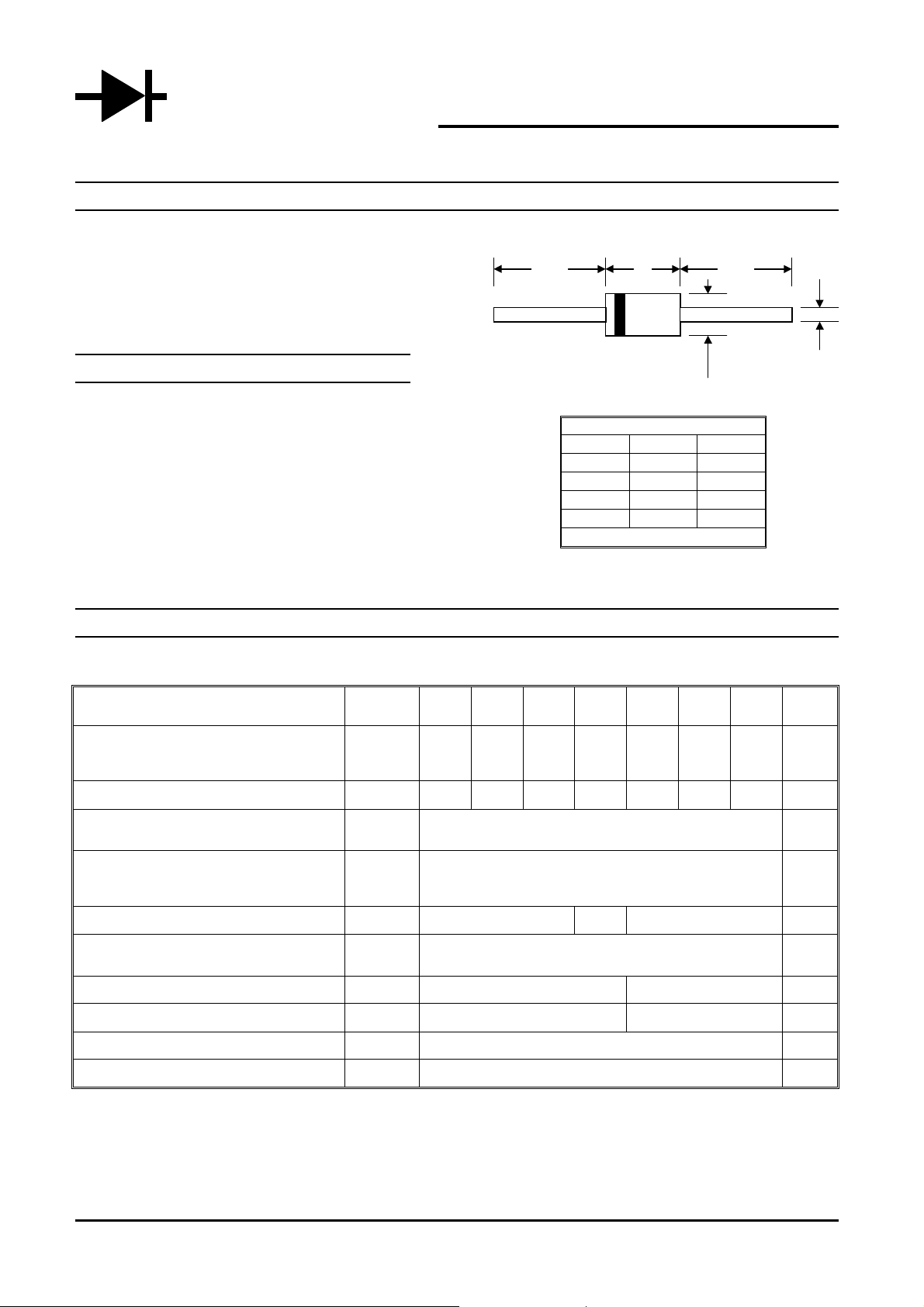
Mechanical Data
C
!
Case: Molded Plastic D
!
Terminals: Plated Leads Solderable per
MIL-STD-202, Method 208
!
Polarity: Cathode Band
!
Weight: 0.34 grams (approx.)
!
Mounting Position: Any
!
Marking: Type Number
Maximum Ratings and Electrical Characteristics
@T
A
=25°C unless otherwise specified
Single Phase, half wave, 60Hz, resistive or inductive load.
For capacitive load, derate current by 20%.
Characteristic Symbol
UF
4001
UF
4002
UF
4003
UF
4004
UF
4005
UF
4006
UF
4007
Unit
Peak Repetitive Reverse Voltage
Working Peak Reverse Voltage
DC Blocking Voltage
V
RRM
V
RWM
V
R
50 100 200 400 600 800 1000 V
RMS Reverse Voltage V
R(RMS)
35 70 140 280 420 560 700 V
Average Rectified Output Current
(Note 1) @T
A
= 55°C
I
O
1.0 A
Non-Repetitive Peak Forward Surge Current
8.3ms Single half sine-wave superimposed on
rated load (JEDEC Method)
I
FSM
30 A
Forward Voltage @I
F
= 1.0A V
FM
1.0 1.3 1.7 V
Peak Reverse Current @T
A
= 25°C
At Rated DC Blocking Voltage @T
A
= 100°C
I
RM
5.0
100
µA
Reverse Recovery Time (Note 2) t
rr
50 75 nS
Typical Junction Capacitance (Note 3) C
j
20 10 pF
Operating Temperature Range T
j
-65 to +125 °C
Storage Temperature Range T
STG
-65 to +150 °C
*Glass passivated forms are available upon request
Note: 1. Leads maintained at ambient temperature at a distance of 9.5mm from the case
2. Measured with IF = 0.5A, IR = 1.0A, IRR = 0.25A. See figure 5.
3. Measured at 1.0 MHz and applied reverse voltage of 4.0V D.C.
WTE
POWER SEMICONDUCTORS
DO-41
Dim Min Max
A
25.4 —
B
4.06 5.21
C
0.71 0.864
D
2.00 2.72
All Dimensions in mm
 Loading...