

White Electronic Designs WEDF1M32B-120HC5A, WEDF1M32B-120HC5, WEDF1M32B-120G2TM5A, WEDF1M32B-120G2TM5, WEDF1M32B-120G2TI5A Datasheet
...
1
White Electronic Designs Corporation • Phoenix, AZ • (602) 437-1520
HI-RELIABILITY PRODUCT
1Mx32 5V FLASH MODULE
ADVANCED*
■ Organized as 1Mx32, user configurable as 2Mx16 or 4Mx8.
■ Commercial, Industrial and Military Temperature Ranges
■ 5V ± 10% for Read and Write Operations.
■ Low Power CMOS
■ Embedded Erase and Program Algorithm
■ Built-in Decoupling Caps and Multiple Ground Pins for Low
Noise Operation
■ Weight
WEDF1M32B-XG2TX5 - 8 grams typical
WEDF1M32B-XHX5 - 13 grams typical
* This data sheet describes a product that may or may not be under
development and is subject to change or cancellation without notice.
FEATURES
■ Access Times of 70, 90, 120ns
■ Packaging:
• 66 pin, PGA Type, 1.185" square, Hermetic Ceramic HIP
(Package 401)
• 68 lead, 22mm Low Profile CQFP, 4.6mm (0.180"),
(Package 509)
■ Sector Architecture
• One 16KByte Sectors
• Two 8KByte Sectors
• One 32KByte Sectors
• Fifteen 64KByte Sectors
■ 1,000,000 Erase/Program Cycles
WEDF1M32B-XXX5
May 1999 Rev. 1
I/O8
I/O9
I/O10
A14
A16
A11
A0
A18
I/O0
I/O1
I/O2
RESET
CS2
GND
I/O
11
A10
A9
A15
VCC
CS1
A19
I/O3
I/O15
I/O14
I/O13
I/O12
OE
A
17
WE
I/O
7
I/O6
I/O5
I/O4
I/O24
I/O25
I/O26
A7
A12
NC
A
13
A8
I/O16
I/O17
I/O18
VCC
CS4
NC
I/O
27
A4
A5
A6
NC
CS
3
GND
I/O
19
I/O31
I/O30
I/O29
I/O28
A1
A2
A3
I/O23
I/O22
I/O21
I/O20
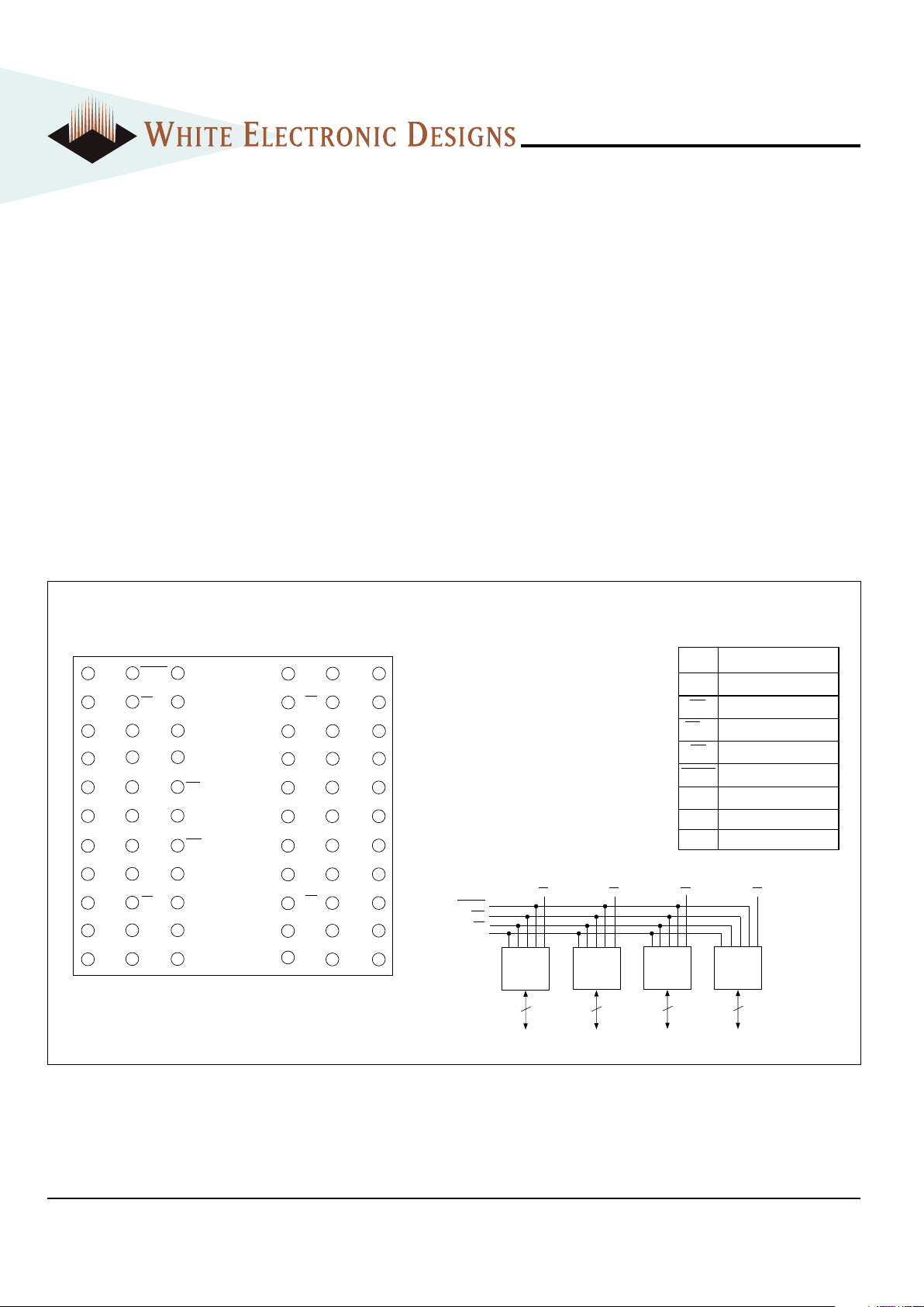
11 22 33 44 55 66
1 12 23 34 45 56
FIG. 1 PIN CONFIGURATION FOR WEDF1M32B-XHX5
PIN DESCRIPTION
TOP VIEW
I/O0-31 Data Inputs/Outputs
A0-19 Address Inputs
WE Write Enable
CS1-4 Chip Selects
OE Output Enable
RESET Reset
VCC Power Supply
GND Ground
NC Not Connected
BLOCK DIAGRAM
1M x 8
8
I/O
0-7
CS
1
1M x 8
8
I/O
8-15
CS
2
1M x 8
8
I/O
16-23
CS
3
1M x 8
8
I/O
24-31
CS
4
A0-
19
OE
WE
RESET
2
White Electronic Designs Corporation • Phoenix, AZ • (602) 437-1520
WEDF1M32B-XXX5
10
11
12
13
14
15
16
17
18
19
20
21
22
23
24
25
26
60
59
58
57
56
55
54
53
52
51
50
49
48
47
46
45
44
9 8 7 6 5 4 3 2 1 68 67 66 65 64 63 62 61
27 28 29 30 31 32 33 34 35 36 37 38 39 40 41 42 43
I/O
0
I/O
1
I/O
2
I/O
3
I/O
4
I/O
5
I/O
6
I/O
7
GND
I/O
8
I/O
9
I/O
10
I/O
11
I/O
12
I/O
13
I/O
14
I/O
15
V
CC
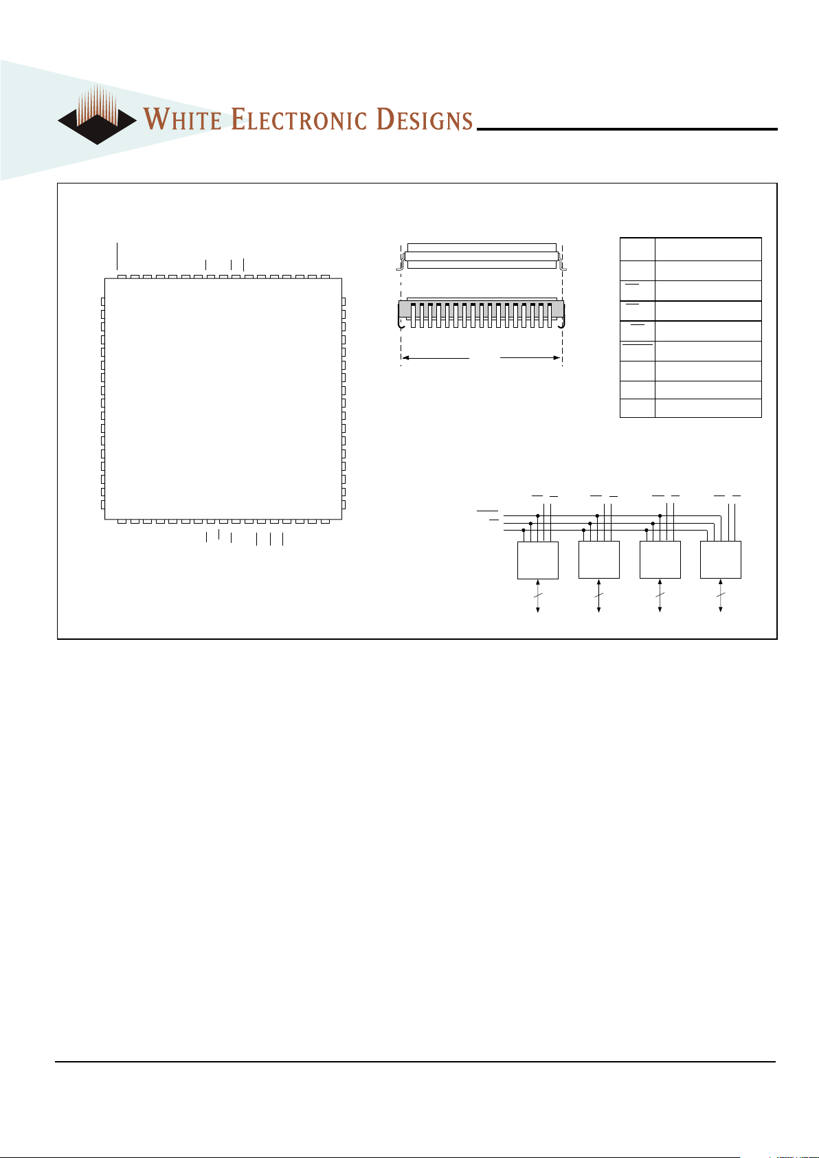
A11A12A13A14A15A
16
CS
1
OE
CS
2
A
17
WE2WE3WE
4
A18A
19
NC
I/O
16
I/O
17
I/O
18
I/O
19
I/O
20
I/O
21
I/O
22
I/O
23
GND
I/O
24
I/O
25
I/O
26
I/O
27
I/O
28
I/O
29
I/O
30
I/O
31
RESET
A0A1A2A3A4A5CS3GND
CS4WE1A6A7A8A9A10V
CC
FIG. 2 PIN CONFIGURATION FOR WEDF1M32B-XG2TX5
TOP VIEW
The White 68 lead G2T CQFP
fills the same fit and function as
the JEDEC 68 lead CQFJ or 68
PLCC. But the G2T has the TCE
and lead inspection advantage
of the CQFP form.
0.940"
1M x 8
8
I/O
0-7
1M x 8
8
I/O
8-15
1M x 8
8
I/O
16-23
1M x 8
8
I/O
24-31
CS
4
A0-
19
OE
RESET
CS
3
CS
2
CS
1
WE
4
WE
3
WE
2
WE
1
BLOCK DIAGRAM
PIN DESCRIPTION
I/O0-31 Data Inputs/Outputs
A0-19 Address Inputs
WE1-4 Write Enables
CS1-4 Chip Selects
OE Output Enable
RESET Reset
VCC Power Supply
GND Ground
NC Not Connected
3
White Electronic Designs Corporation • Phoenix, AZ • (602) 437-1520
WEDF1M32B-XXX5
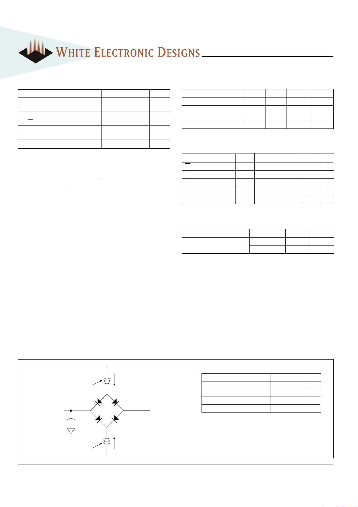
FIG. 3
AC TEST CIRCUIT
NOTES:
V
Z is programmable from -2V to +7V.
I
OL & IOH programmable from 0 to 16mA.
Tester Impedance Z
0 = 75 Ω.
V
Z is typically the midpoint of VOH and VOL.
I
OL & IOH
are adjusted to simulate a typical resistive load circuit.
ATE tester includes jig capacitance.
AC TEST CONDITIONS
I
Current Source
D.U.T.
C = 50 pf
eff
I
OL
V ≈ 1.5V
(Bipolar Supply)
Z
Current Source
OH
RECOMMENDED OPERATING CONDITIONS
Parameter Symbol Min Max Unit
Supply Voltage VCC 4.5 5.5 V
Input High Voltage VIH 2.0 VCC + 0.5 V
Input Low Voltage VIL -0.5 +0.8 V
Operating Temp. (Mil.) T
A -55 +125 °C
Parameter Typ Unit
Input Pulse Levels
VIL = 0, VIH = 3.0
V
Input Rise and Fall 5 ns
Input and Output Reference Level 1.5 V
Output Timing Reference Level 1.5 V
CAPACITANCE
(TA = +25°C)
Parameter
Symbol
Conditions Max Unit
OE capacitance COE
VIN = 0 V, f = 1.0 MHz
50 pF
WE1-4 capacitance CWE
VIN = 0 V, f = 1.0 MHz
20 pF
CS1-4 capacitance CCS
VIN = 0 V, f = 1.0 MHz
20 pF
Data I/O capacitance CI/O
V
I/O
= 0 V, f = 1.0 MHz
20 pF
Address input capacitance C
ADVIN
= 0 V, f = 1.0 MHz
50 pF
This parameter is guaranteed by design but not tested.
ABSOLUTE MAXIMUM RATINGS
NOTES:
1. Minimum DC voltage is -0.5V on input/output pins. During transitions, this
level may undershoot to -2.0V for periods <20ns. Maximum DC voltage on
input/output pins is V
CC + 0.5V which, during transitions, may overshoot to
V
CC + 2.0V for periods <20ns.
2. Minimum DC input voltage on pins A
9, OE, and RESET is -0.5V. During
voltage transitions, A
9, OE, and RESET may undershoot Vss to -2.0V for
periods of up to 20ns. See Figure 6. Maximum DC input voltage on pin A
9 is
+12.5V which may overshoot to +13.5V for periods up to 20ns.
3. Output shorted for no more than one second. No more than one output
shorted at a time.
Stresses above those listed under “Absolute Maximum Ratings” may cause
permanent damage to the device. This is a Stress rating only and functional
operation of the device at these or any other conditions above those indicated in
the operational sections of this specification is not implied. Exposure to absolute
maximum rating conditions for extended periods may affect device reliability.
Parameter Unit
Voltage on Any Pin with Respect to -0.5 to +7.0 V
GND – VCC and VPP)
Voltage with Respect to GND – -2.0 to +12.5 V
A9, OE, and RESET (2)
Voltage with Respect to GND – -2.0 to +7.0 V
All other pins (1)
Output Short Circuit Current 200 mA
DATA RETENTION
Parameter Test Conditions Min Unit
Minimum Pattern Data 150°C 10 Years
Retention Time 125°C 20 Years

4
White Electronic Designs Corporation • Phoenix, AZ • (602) 437-1520
DC CHARACTERISTICS - CMOS COMPATIBLE
(V
CC = 5.0V, GND = 0V, TA = -55°C to +125°C)
NOTES:
1. The Icc current listed is typically less than 2mA/MHz, with OE at V
IH.
2. Maximum Icc specifications are tested with V
CC = VCC max.
3. I
CC active while Embedded Erase or Embedded Program is in progress.
4. Not 100% tested.
5. ICC3 = 20µA max at extended temperature (> +85°C).
Parameter Symbol Conditions Min Max Unit
Input Leakage Current ILI VIN = VCC to GND 10 µA
Output Leakage Current ILO VOUT = VCC to GND 10 µA
VCC Read Current (1,2) ICC1 CS = VIL, OE VIH, f = 5 MHz, IOUT = 0mA 160 mA
VCC Write Current (2,3,4) ICC2 CS = VIL, OE VIH 200 mA
VCC Standby Current (2,5) ICC3 CS = RESET = OE = VIH, f = 5MHz 20.0 mA
Output Low Voltage VOL VCC = 4.5, IOL = 5.8 mA 0.45 V
Output High Voltage VOH VCC = 4.5, IOH = -2.5 mA 2.4 V
Low V
CC Lockout Voltage (4) VLKO 3.2 4.2 V
AC CHARACTERISTICS – WRITE/ERASE/PROGRAM OPERATIONS - WE CONTROLLED
(V
CC = 5.0V, GND = 0V, TA = -55°C to +125°C)
Parameter Symbol -70 -90 -120 Unit
Min Max Min Max Min Max
Write Cycle Time tAVAV tWC 70 90 120 ns
Chip Select Setup Time tELWL tCS 00 0 ns
Write Enable Pulse Width tWLWH tWP 35 45 50 ns
Address Setup Time tAVWH tAS 00 0 ns
Data Setup Time tDVWH tDS 30 45 50 ns
Data Hold Time tWHDX tDH 00 0 ns
Address Hold Time tWHAX tAH 45 45 50 ns
Chip Select Hold Time tWHEH tCH 00 0 ns
Write Enable Pulse Width High tWHWL tWPH 20 20 20 ns
Programming Operation (2) tWHWH1 300 300 300 µs
Sector Erase Operation (3) tWHWH2 888sec
Write Recovery before Read tWHGL 00 0 µs
Chip Programming Time 50 50 50 sec
NOTES:
1. Guaranteed by design, not tested.
2. Typical value for t
WHWH1 is 7µs.
3. Typical value for tWHWH2 is 1sec.
WEDF1M32B-XXX5
5
White Electronic Designs Corporation • Phoenix, AZ • (602) 437-1520
NOTES:
1. Typical value for t
WHWH1 is 7µs.
2. Typical value for tWHWH2 is 1sec.
Parameter Symbol -70 -90 -120 Unit
Min Max Min Max Min Max
Write Enable Cycle Time tAVAV tWC 70 90 120 ns
Write Enable Setup Time tWLEL tWS 00 0ns
Chip Select Pulse Width tELEH tCP 35 45 50 ns
Address Setup Time tAVEH tAS 00 0ns
Data Setup Time tDVEH tDS 30 45 50 ns
Data Hold Time tEHDX tDH 00 5ns
Address Hold Time tEHAX tAH 45 45 50 ns
Write Enable Hold Time tEHWH tWH 00 0ns
Chip Select Pulse Width High tEHEL tEPH 20 20 20 ns
Programming Operation (1) tWHWH1 300 300 300 µs
Sector Erase Operation (2) tWHWH2 8 8 8 sec
Write Recovery before Read t
EHGL 00 0µs
AC CHARACTERISTICS – WRITE OPERATION - CS CONTROLLED
(1)
(VCC = 5.0V, GND = 0V, TA = -55°C to +125°C)
AC CHARACTERISTICS – READ-ONLY OPERATIONS
(VCC = 5.0V, GND = 0V, TA = -55°C to +125°C)
Parameter Symbol -70 -90 -120 Unit
Min Max Min Max Min Max
Read Cycle Time tAVAV tRC 70 90 120 ns
Address Access Time tAVQV tACC 70 90 120 ns
Chip Select to Output Valid (1) tELQV tCE 70 90 120 ns
Output Enable to Output Valid (1) tGLQV tOE 30 35 50 ns
Chip Select to Output Low Z (2) tELQX tLZ 000ns
Chip Select High to Output High Z (2) tEHQZ tHZ 20 20 50 ns
Output Enable to Output Low Z (2) tGLOX tOLZ 000ns
Output Enable High to Output High Z (2) tGHQZ tDF 20 20 30 ns
Output Hold from Addresses, CS or OE t
OH 000ns
Change, Whichever is First (2)
NOTES:
1. OE may be delayed up to t
CE-tOE after the falling edge of CS without impact on tCS.
2. Guaranteed by design, not tested.
WEDF1M32B-XXX5

6
White Electronic Designs Corporation • Phoenix, AZ • (602) 437-1520
PACKAGE 509: 68 LEAD, LOW PROFILE CERAMIC QUAD FLAT PACK, CQFP (G2T)
0.38 (0.015) ± 0.05 (0.002)
0.27 (0.011) ± 0.04 (0.002)
25.15 (0.990) ± 0.26 (0.010) SQ
1.27 (0.050) TYP
24.03 (0.946)
± 0.26 (0.010)
22.36 (0.880) ± 0.26 (0.010) SQ
20.3 (0.800) REF
4.57 (0.180) MAX
0.19 (0.007)
± 0.06 (0.002)
23.87
(0.940) REF
1.0 (0.040)
± 0.127 (0.005)
0.25 (0.010) REF
1° / 7°
R 0.25
(0.010)
DETAIL A
SEE DETAIL "A"
Pin 1
ALL LINEAR DIMENSIONS ARE MILLIMETERS AND PARENTHETICALLY IN INCHES
0.940"
TYP
The White 68 lead G2T CQFP
fills the same fit and function as
the JEDEC 68 lead CQFJ or 68
PLCC. But the G2T has the TCE
and lead inspection advantage
of the CQFP form.
WEDF1M32B-XXX5

7
White Electronic Designs Corporation • Phoenix, AZ • (602) 437-1520
PACKAGE 401: 66 PIN, PGA TYPE, CERAMIC HEX-IN-LINE PACKAGE, HIP (H)
30.1 (1.185) ± 0.38 (0.015) SQ
25.4 (1.0) TYP
15.24 (0.600) TYP
0.76 (0.030) ± 0.1 (0.005)
6.22 (0.245)
MAX
3.81 (0.150)
± 0.1 (0.005)
2.54 (0.100)
TYP
25.4 (1.0) TYP
1.27 (0.050) ± 0.1 (0.005)
1.27 (0.050) TYP DIA
0.46 (0.018) ± 0.05 (0.002) DIA
PIN 1 IDENTIFIER
SQUARE PAD
ON BOTTOM
ALL LINEAR DIMENSIONS ARE MILLIMETERS AND PARENTHETICALLY IN INCHES
WEDF1M32B-XXX5

8
White Electronic Designs Corporation • Phoenix, AZ • (602) 437-1520
LEAD FINISH:
Blank = Gold plated leads
A = Solder dip leads
V
PP PROGRAMMING VOLTAGE
5 = 5V
DEVICE GRADE:
M= Military Screened -55°C to +125°C
I = Industrial -40°C to +85°C
C = Commercial 0°C to +70°C
PACKAGE TYPE:
H = Ceramic Hex-In-Line Package, HIP (Package 401)
G2T = 22mm Ceramic Quad Flat Pack, Low Profile CQFP (Package 509)
ACCESS TIME (ns)
Bottom Boot Block
ORGANIZATION, 1M x 32
User configurable as 2M x 16 or 4M x 8
Flash
WHITE ELECTRONIC DESIGNS CORP.
ORDERING INFORMATION
WED F 1M32 B - XXX X X 5 X
WEDF1M32B-XXX5
 Loading...