

White Electronic Designs EDI8L24128C15BC, EDI8L24128C12BI, EDI8L24128C12BC Datasheet
EDI8L24128C
128Kx24 Asynchronous SR128Kx24 Asynchronous SR
128Kx24 Asynchronous SR
128Kx24 Asynchronous SR128Kx24 Asynchronous SR
FEATURES
n 128Kx24 bit CMOS Static
n Random Access Memory Array
• Fast Access Times: 12 and 15ns
• Master Output Enable and Write Control
• TTL Compatible Inputs and Outputs
• Fully Static, No Clocks
n Surface Mount Package
• 119 Lead BGA (JEDEC MO-163), No. 391
• Small Footprint, 14mm x 22mm
• Multiple Ground Pins for Maximum Noise Immunity
n Single +5V (±10%) Supply Operation
n DSP Memory Solution
• Motorola DSP5600x™
• Analog Devices SHARC™
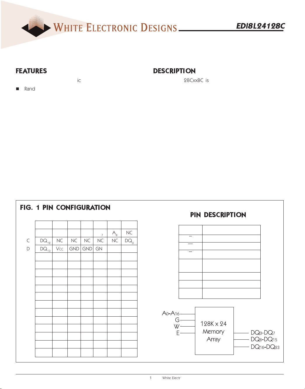
FIG. 1 PIN CONFIGURATION
1234567
ANCA
BNCA
CDQ
12
DDQ13VCC GND GND GND VCC DQ
EDQ14GND VCC GND VCC GND DQ
FDQ15VCC GND GND GND VCC DQ
GDQ16GND VCC GND VCC GND DQ
HDQ17VCC GND GND GND VCC DQ
I NC GND VCC GND VCC GND NC
JDQ
18
KDQ19GND VCC GND VCC GND DQ
LDQ20VCC GND GND GND VCC DQ
MDQ21GND VCC GND VCC GND DQ
NDQ22VCC GND GND GND VCC DQ
ODQ23NC NC NC NC NC DQ
PNCA9A10WA11A12NC
QNCA
A1A2A3A4NC
0
A6EA7A8NC
5
NC NC NC NC NC DQ
VCC GND GND GND VCC DQ
13A14
GA15A16NC
AM, 5VAM, 5V
AM, 5V
AM, 5VAM, 5V
DESCRIPTION
The EDI8L24128CxxBC is a 5V, three megabit SRAM constructed with three 128Kx8 die mounted on a multi-layer
laminate substrate. With 12 to 15ns access times, x24 width
and a 5V operating voltage, the EDI8L2418C is ideal for
creating a single chip memory solution for the Motorola
DSP5600x or a two chip solution for the Analog Devices
SHARC™ DSP.
The single or dual chip memory solutions offer improved
system performance by reducing the length of board traces
and the number of board connections compared to using
multiple monolithic devices. For example, the capacitance
load on the data lines for the BGA package is 58% less than
a monolithic SOJ solution.
The JEDEC Standard 119 lead BGA provides a 44% space
savings over using 128Kx8, 300mm wide SOJs and the BGA
package has a height of 100mm compared to 148mm for
the SOJ packages.
0
1
2
3
4
5
6
7
8
9
10
11
PIN DESCRIPTION
A
0-16
E Chip Enables
W Master Write Enable
G Master Output Enable
DQ
0-23
VCC Power (+5V±10%)
GND Ground
NC No Connection
Address Inputs
Common Data
Input/Output
January 2002 Rev. 1
ECO# 14691
White Electronic Designs Corporation • (508) 366-5151 • www.whiteedc.com
1
EDI8L24128C
ABSOLUTE MAXIMUM RATINGS*
Voltage on any pin relative to VSS -0.5V to 7.0V
Operating Temperature TS (Ambient)
Commercial 0°C to + 70°C
Industrial -40°C to +85°C
Storage Temperature -55°C to +125°C
Power Dissipation 3 Watts
Output Current. 20 mA
Junction Temperature, TJ 175°C
*Stress greater than those listed under "Absolute Maximum Ratings" may
cause permanent damage to the device. This is a stress rating only and
functional operation of the device at these or any other conditions greater
than those indicated in the operational sections of this specification is not
implied. Exposure to absolute maximum rating conditions for extended
periods may affect reliability.
TRUTH TABLE
E W G Mode Output Power
H X X Standby High Z ICC2, ICC
L H H Output Deselect High Z ICC
L H L Read Data Out ICC
L L X Write Data In ICC
1
1
1
DC ELECTRIC AL CHARACTERISTICS
(VCC = 5V, TA = 25°C)
RECOMMENDED OPERATING
CONDITIONS
Parameter Symbol Min Typ Max Units
Supply Voltage VCC 4.5 5.0 5.5 V
Supply Voltage VSS 00 0V
Input High Voltage VIH 2.2 — VCC+0.3 V
Input Low Voltage VIL -0.3 — +0.8 V
CAPACITANCE
(f=1.0MHZ, VIN=VCC OR VSS)
Parameter Symbol Max Unit
Address Lines CL 8pf
Data Lines CD/Q 10 pf
Write & Output Enable Line W, G 8 pf
Chip Enable Lines E 8 pf
3
Parameter Symbol Conditions Min Type Max Units
Operating Power Supply Current ICC
Standby (TTL) Power Supply Current ICC
Full Standby Power CMOS ICC
Supply Current VIN ³ VCC -0.2V or VIN £ 0.2V
Input Leakage Current ILI VIN = 0V to VCC — — ±10 mA
Output Leakage Current ILO VI/O 0V to VCC — — ±10 mA
Output High Voltage VOH IOH = -4.0mA 2.4 — — V
Output Low Voltage VOL IOL = 8.0mA — — 0.4 V
W = VIL, II/O = 0mA, Min Cycle 200 270 mA
1
E ³ VIH, VIN £ VIL or VIN ³ VIH,45mA
2
f = 0MHz
E ³ VCC -0.2V
3
10 mA
AC TEST CONDITIONS
FIG. 1
White Electronic Designs Corporation • Westborough, MA • (508) 366-5151
FIG. 2
2
Input Pulse Levels VSS to 3.0V
Input Rise and Fall Times 5ns
Input and Output Timing Levels 1.5V
Output Load Figure 1
Note: For tEHQZ, tGHQZ and tWLQZ, CL = 5pF Figure 2
 Loading...