

查询BQ2007供应商
Features
Fast charging and conditioning of
➤
NiCd and NiMH batteries
Precise charging independent
-
of battery pack number of cells
Discharge-before-charge on
-
demand
Pulse trickle charge
-
conditioning
Battery undervoltage and
-
overvoltage protection
Built-in 10-step voltage-based
➤
charge status monitoring
Charge status display options
-
include seven-segment
monotonic bargraph and fully
decoded BCD digit
Display interface options for
-
direct drive of LCD or LED
segments
-
Charger state status
indicators for pending,
discharge, charge, completion,
and fault
Audible alarm for charge
-
completion and fault
conditions
Charge control flexibility
➤
Fast or Standard speed
-
charging
Top-off mode for NiMH
-
Charge rates from
-
C
to 2C
8
(30 minutes to 8 hours)
Charge termination by:
➤
Negative delta voltage (-∆V)
-
Peak voltage detect (PVD)
-
Maximum voltage
-
Maximum time
-
Maximum temperature
-
➤ High-efficiency switch-mode de-
sign
Ideal for small heat-sensitive
-
enclosures
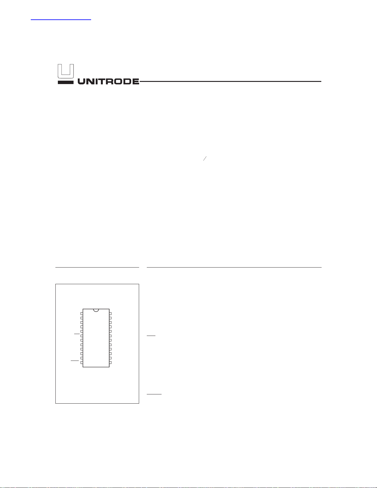
➤ 24-pin,300-mil SOIC or DIP
bq2007
Fast-Charge IC
General Description
The bq2007 is a highly integrated
monolithic CMOS IC designed to pro
vide intelligent battery charging and
charge status monitoring for standalone charge systems.
The bq2007 provides a wide variety of
charge status display formats. The
bq2007 internal charge status moni
tor supports up to a seven-segment
bargraph or a single BCD digit dis
play. The bargraph display indicates
up to seven monotonic steps, whereas
the BCD digit counts in ten steps of
10% increments. The bq2007 output
drivers can direct-drive either an
LCD or LED display.
Charge action begins either by application of the charging supply or by
replacement of the battery pack. For
safety, charging is inhibited until
battery temperature and voltage are
within configured limits.
-
-
-
Pin Connections Pin Names
SEGC/ Display output segment C/
MSEL driver mode select
SEGC/MSEL
9/96 B
SEG
SEG
LED
LED
INH
COM
ALARM
VSEL
FAST
DCMD
TM
1
2
B
3
A
4
1
5
2
6
7
8
9
10
11
12
24-Pin Narrow DIP
or SOIC
24
23
22
21
20
19
18
17
16
15
14
13
PN200701.eps
SEGD/DSEL
SEGE/DSEL
SEGF/MULT
SEGG/QDSEL
MOD
V
CC
V
SS
DIS
TS
BAT
SNS
TCO
SEG
SEG
1
2
LED
LED
INH
COM Common LED/LCD output
ALARM Audio alarm output
TM Timer mode select
VSEL Voltage termination select
FAST Fast charge rate select
DCMD
TCO Temperature cutoff
Display output segment B
B
Display output segment A
A
Charge status output 1
1
Charge status output 2
2
Charge inhibit input
Discharge command
SNS Sense resistor input
BAT Battery voltage
TS Temperature sense
DIS Discharge control
V
SS
V
CC
System ground
5.0V±10% power
MOD Modulation control
SEG
/ Display output segment G/
G
QDSEL charge status display select
SEG
/ Display output segment F/
F
MULT multi-cell pack select
SEG
/ Display output segment E/
E
DSEL
SEG
DSEL
display select 2
2
/ Display output segment D/
D
display select 1
1
1

bq2007
The acceptable battery temperature range is set by an
internal low-temperature threshold and an external
high-temperature cutoff threshold. The absolute tem
perature is monitored as a voltage on the TS pin with
the external thermistor network shown in Figure 2.
The bq2007 provides for undervoltage battery protection
from high-current charging if the battery voltage is less
than the normal end-of-discharge value. In the case of a
deeply discharged battery, the bq2007 enters the
charge-pending state and attempts trickle-current condi
tioning of the battery until the voltage increases. Should
the battery voltage fail to increase above the discharge
value during the undervoltage time-out period, a fault
condition is indicated.
Discharge-before-charge may be selected to automatically
discharge the battery pack on battery insertion or with a
push-button switch. Discharge-before-charge on demand
provides conditioning services that are useful to correct or
prevent the NiCd voltage depression, or “memory” effect,
and also provide a zero capacity reference for accurate
capacity monitoring.
After prequalification and any required dischargebefore-charge operations, charge action begins until one of
the full-charge termination conditions is detected. The
bq2007 terminates charging by any of the following methods:
n Negative delta voltage (-
n
Peak voltage detect (PVD)
n
Maximum absolute temperature
n
Maximum battery voltage
n
Maximum charge time-out
V)
∆
The bq2007 may be programmed for negative delta
voltage (-∆V) or peak voltage detect (PVD) charge
termination algorithms. The VSEL input pin selects -∆V
or PVD termination to match the charge rate and
battery characteristics.
To provide maximum safety for battery and system,
charging terminates based on maximum temperature
cutoff (TCO), maximum cutoff voltage (MCV), and
maximum time-out (MTO). The TCO threshold is the
maximum battery temperature limit for charging. TCO
terminates charge action when the temperature sense
input voltage on the TS pin drops below the TCO pin
voltage threshold. MCV provides battery overvoltage
protection by detecting when the battery cell voltage
(V
CELL=VBAT-VSNS
) exceeds the VMCV value and ter
minates fast charge, standard charge, or top-off charge.
The maximum time-out (MTO) termination occurs when
the charger safety timer has completed during the active
charge state.
The bq2007 indicates charge state status with an audio
alarm output option and two dedicated output pins with pro
grammable display options. The DSEL1–2 inputs can select
-
one of the three display modes for the LED1–2 outputs.
Charger status is indicated for:
Charge pending
n
Charge in progress
n
Charge complete
-
n
Fault condition
n
Pin Descriptions
SEG
MSEL
DSEL
DSEL
MULT
QDSEL
LED
LED
-
INH
Display output segments A–G
A–G
State-of-charge monitoring outputs. QDSEL
input selects the bargraph or BCD digit dis
play mode. See Table 3.
Display driver mode select
Soft-programmed input selects LED or LCD
driver configuration at initialization. When
MSEL is pulled up to V
, outputs SEG
CC
LED interface levels; when MSEL is pulled
down to V
Display mode select 1–2
–
1
2
, outputs SEG
SS
are LCD levels.
A–G
Soft-programmed inputs control the LED
charger status display modes at initialization.
See Table 2.
Fixed-cell pack select
Soft-programmed input is pulled up to V
when charging multi-cell packs and is pulled
down to V
for charging packs with a fixed
SS
number of cells.
State-of-charge display select
The QDSEL input controls the SEG
state-of-charge display modes. See Table 3.
Charger status outputs 1–2
–
1
2
Charger status output drivers for direct
drive of LED displays. Display modes are
selected by the DSEL input. See Table 2.
Charge inhibit input
When low, the bq2007 suspends all charge ac
tions, drives all outputs to high impedance, and
assumes a low-power operational state. When
transitioning from low to high, a charge
cycle is initiated. See page 10 for details.
A–G
-
-
are
1—2
CC
A–G
-
2

bq2007
COM
ALARM
TM
VSEL
FAST
DCMD
TCO
SNS
BAT
Common LCD/LED output
Common output for LCD/LED display
SEG
initialization to allow reading of
soft-programmed inputs DSEL
MSEL, MULT, and QDSEL.
Audio output
Audio alarm output.
Timer mode select
TM is a three-level input that controls the set
tings for charge control functions. See Table 5.
Voltage termination select
This input switches the voltage detect
sensitivity. See Table 5.
Fast charge rate select
The FAST input switches between Fast and
Standard charge rates. See Table 4.
Discharge command
The DCMD
before-charge function. A negative-going
pulse initiates a discharge action. If DCMD
is connected to VSS, automatic dischargebefore-charge is enabled. See Figure 3.
Temperature cut-off threshold input
Minimum allowable battery temperaturesensor voltage. If the potential between TS
and SNS is less than the voltage at the TCO
input, then any fast charging or top-off
charging is terminated.
Sense resistor input
SNS controls the switching of MOD output based
on an external sense resistor. This provides the
lower reference potential for the BAT pin and the
TS pin.
Battery voltage input
Battery voltage sense input referenced to SNS
for the battery pack being charged. This resis
tor divider network is connected between the
positive and the negative terminals of the
battery. See Figure 1.
. Output is high-impedance during
A—G
, DSEL2,
1
input controls the discharge-
TS
DIS
V
SS
-
V
CC
MOD
Temperature sense input
Input referenced to SNS for battery tem
perature monitoring negative temperature
coefficient (NTC) thermistor.
Discharge control
DIS is a push-pull output that controls an
external transistor to discharge the battery
before charging.
Ground
VCCsupply input
Current-switching control output
Push/pull output that controls the charging
current to the battery. MOD switches high to
enable current flow and low to inhibit current
flow.
Functional Description
Figure 1 illustrates charge control and display status
during a bq2007 charge cycle. Table 1 summarizes the
bq2007 operational features. The charge action states
and control outputs are given for possible input
conditions.
Charge Action Control
The bq2007 charge action is controlled by input pins
DCMD
, VSEL, FAST, and TM. When charge action is
initiated, the bq2007 enters the charge-pending state,
checks for acceptable battery voltage and temperature,
and performs any required discharge-before-charge
operations. DCMD
function, and VSEL, FAST, and TM select the charger
configuration. See Tables 4 and 5.
During charging, the bq2007 continuously tests for
charge termination conditions: negative delta voltage,
peak voltage detection, maximum time-out, battery
over-voltage, and high-temperature cutoff. When the
charge state is terminated, a trickle charge continues to
compensate for self-discharge and maintain the fully
charged condition.
Charge Status Indication
-
Table 2 summarizes the bq2007 charge status display
indications. The charge status indicators include the
DIS output, which can be used to indicate the discharge
state, the audio ALARM output, which indicates charge
completion and fault conditions, and the dedicated
status outputs,LED
controls the discharge-before-charge
and LED2.
1
-
3
bq2007
Charge
Pending
(Pulse-Trickle)
Dis-
charge
(Optional)
DIS
MOD
or
MOD
(Switching
Configuration)
(External
Regulation)
Mode 1, LED2 Status Output
Mode 1, LED1 Status Output
Mode 2, LED2 Status Output
Mode 2, LED1 Status Output
Mode 3, LED2 Status Output
Fast Charging
Top-Off
(Optional)
260 s
2080 s
260 s
2080 s
Pulse-Trickle
Note
260 s
Note
260 s
Mode 3, LED1 Status Output
Battery discharged to V
temperature/voltage limits. (Discharge-before-charge not
qualified by temperature.)
Low-voltage fault: Battery voltage less than V
Charge initiated. Battery outside temperature/voltage limits.
Note: See Table 4 for pulse-trickle period.
Figure 1. Example Charging Action Events
4
or battery within
EDV
for under-voltage time-out.
EDV
TD200701.eps

bq2007
Outputs LED
selected at initialization by the input pins DSEL
DSEL
. The DSEL1and DSEL2input pins, when pulled
2
down to V
simple two-LED system. LED
status (i.e., charge pending and discharge) and LED
have three display modes that are
1–2
, are intended for implementation of a
SS
indicates the precharge
2
and
1
indi
1
cates the charge status (i.e., charging and completion).
DSEL
pulled up to VCCand DSEL2pulled down to V
1
mode is for implementation of a single tri-color LED such
that discharge, charging, and completion each have a unique
color. DSEL
V
allows for fault status information to be displayed.
CC
pulled down to VSSand DSEL2pulled up to
1
Audio Output Alarm
The bq2007 audio alarm output generates an audio tone
to indicate a charge completion or fault condition. The
audio alarm output is a symmetrical duty-cycle AC sig
nal that is compatible with standard piezoelectric alarm
elements. A valid battery insertion is indicated by a sin
gle high-tone beep of
charge completion and fault conditions are indicated by
a 9.5- to 15-second high-tone sequence of
cal duration at a 2-second typical repetition rate.
Charge Action
State Conditions MOD Output DIS Output
Battery absent V
Charge initiation
Discharge-beforecharge
Charge pending
Fast charging
Standard charging
Charge complete
Top-off pending
Top-off charging
Trickle charging
Fault
Definitions: V
1
-second typical duration. The
2
1
2
Table 1. bq2007 Operational Summary
applied and V
CC
V
applied or V
CC
from≥V
DCMD
high-to-low transition or to VSSon charge
initiation and V
Charge initiation occurred and V
V
Charge pending complete and FAST = V
Charge pending complete and FAST = V
-∆V termination or V
-3mV/cell or maximum time-out or V
VSEL = V
or V
VSEL = V
time-out not exceeded and V
Charge complete and top-off disabled or
Charge pending state and charge pending
= V
V
CELL
LTF
= 0.5*VCC.
BAT
- V
V
≤
TEMP
CC
TCO
, charge complete and V
V
≤
TEMP
and charge complete and
CC
V
CELL
top-off complete or pending
time-out (t
SNS;VMCV
= 0.8*VCC;V
-second typi-
CELL
CELL
to < V
MCV
< V
EDV
CELL
or V
CELL
< V
TEMP
TCO
PEND
or V
CELL
< V
MCV
) complete
TCO
TEMP
Charge Status Monitoring
The bq2007 charge status monitor may display the bat
tery voltage or charge safety timer as a percentage of
the full-charged condition. These options are selected
-
with the MULT soft-programmed input pin.
When MULT is pulled down to V
SS
status is displayed as a percentage of the battery
voltage, and the single-cell battery voltage at the BAT
pin is compared with internal charge voltage reference
thresholds. When V
thresholds of V
20,V40,V60
is greater than the internal
BAT
,orV80, the respective 20%,
40%, 60%, or 80% display outputs are activated. The
battery voltage directly indicates 20% charge
increments, while the 10% charge increments use a
timer that is a function of the charge safety timer.
When MULT is pulled down to V
exceeds V20during charging, the 20% charge indication
is activated and the timer begins counting for a period
equal to
When the timer count is completed, the 30% charge
1
1
to
64
of the charge safety time-out period.
32
indication is activated. Should V
the timer count completion, the charge status monitor
activates the 30% and 40% indications. This technique
V
≥
MCV
drops
MCV
< V
MCV
≥
TEMP
< V
EDV
or PVD≥0 to
CELL
TEMP
< V
EDV
> V
TCO
V
LTF
> V
≥
Trickle charge per Table 4 Low
- Low
Low High
or
Trickle charge per Table 4 Low
CC
SS
V
and
Low if V
high if V
Low if V
high if V
MCV
LTF
Trickle charge per Table 4 Low
Activated per V
73ms of every 585ms Low
SNS
SNS
SNS
SNS
--
Trickle charge per Table 4 Low
Trickle charge per Table 4 Low
= 0.262*VCCor 0.4*VCC;V
EDV
, the battery charge
SS
SS
exceed V40prior to
BAT
> 250mV;
< 200mV
> 250mV;
< 200mV
for
SNS
= VTS- V
TEMP
and when V
SNS
-
BAT
Low
Low
;
5

bq2007
is used for all the odd percentage charge indications to
assure a monotonic charge status display.
When MULT is pulled up to V
status monitor directly displays
timer as a percentage of full charge. This method is rec
, the bq2007 charge
CC
1
of the charge safety
32
ommended over the voltage-based method when charg
ing fixed-cell packs where the battery terminal voltages
can vary greatly between packs. This method offers an
accurate charge status indication when the battery is
fully discharged. When using the timer-based method,
discharge-before-charge is recommended.
During discharge with MULT pulled down to V
SS
, the
charge status monitor indicates the percentage of the bat
tery voltage by comparing V
to the internal discharge
BAT
voltage reference thresholds. In BCD format, the dis
charge thresholds V
80,V60,V40
, and V20correspond to a
battery charge state indication of 90%, 70%, 50%, and 30%,
respectively. In bargraph format, the same discharge
thresholds correspond to a battery charge state indication
of 90%, 60%, 40%, and 30%, respectively. Differences in
the battery charge state indications are due to the finer
granularity of the BCD versus the bargraph format.
During discharge and when MULT is pulled up to V
CC
the state-of-charge monitor BCD format displays the
discharge condition, letter “d,” whereas the bargraph format has no indication.
Table 2. bq2007 Charge Status Display Summary
The charge status display is blanked during the charge
pending state and when the battery pack is removed.
Charge Status Display Modes
-
The bq2007 charge status monitor can be displayed in
-
two modes summarized in Table 3. The display modes
are a seven-segment monotonic bargraph or a sevensegment BCD single-digit format. When QDSEL is
pulled down to V
segments of a single BCD digit display, and when QDSEL
is pulled up to V
ments of a bargraph display.
-
In the bargraph display mode, outputs SEG
tions for a three-segment to seven-segment bargraph dis
-
play. The three-segment charge status display uses out
puts SEG
B
charge indications, respectively. The four-segment charge
status display uses outputs SEG
SEG
for 20%, 40%, 60%, and 80% indications,
E
respectively. The seven-segment charge status monitor
uses all segments.
The BCD display mode drives pins SEG
,
decoded seven-segment single-digit information. The
display indicates in 10% increments from a BCD zero
count at charge initiation to a BCD nine count indicating 90% charge capacity. Charge completion is indicated
by the letter “F,” a fault condition by the letter “E,” and
the discharge condition by the letter “d.” See Table 3.
, pins SEG
SS
, pins SEG
CC
drive the decoded seven
A–G
drive the seven seg
A–G
A–G
,SEGD, and SEGFfor 30%, 60%, and 90%
, SEGC, SEGD,and
A
A–G
allow op
with the
-
-
-
-
Mode Charge Action State LED
1
Battery absent 0000
Charge pending (temp. limit, low voltage) 0 Flashing 0 0
DSEL
= L
DSEL
(Mode 1)
1
= L
2
Discharge in progress 0110
Charging Flashing 0 0 0
Charge complete 1 0 0 High tone
Fault (low-voltage time-out) 0 0 0 High tone
Battery absent 0000
DSEL
DSEL
(Mode 2)
1
2
= H
= L
Discharge in progress, pending 1110
Charging 1000
Charge complete 0 1 0 High tone
Fault (low-voltage time-out) 0 0 0 High tone
Battery absent 0000
Charge pending (temp. limit, low voltage) 0 Flashing 0 0
DSEL
= L
DSEL
(Mode 3)
1
2
= H
Discharge in progress 0 Flashing 1 0
Charging Flashing 0 0 0
Charge complete 1 0 0 High tone
Fault (low-voltage time-out) 0 1 0 High tone
Note: 1 = on; 0 = off; L = pulled down to VSS; H = pulled up to VCC.
6
LED
2
DIS ALARM

bq2007
Display Driver Modes
The bq2007 is designed to interface with LCD or LED
type displays. The LED signal levels are driven when
the MSEL soft-programmed input is pulled to V
tialization. The output pin COM is the common anode
connection for LED SEG
A–G
.
The LCD interface mode is enabled when the MSEL
soft-programmed input pin is pulled to V
SS
tion. An internal oscillator generates all the timing sig
nals required for the LCD interface. The output pin
COM is the common connection for static direct-driving
of the LCD display backplane and is driven with an AC
signal at the frame period. When enabled, each of the
SEG
pins is driven with the correct-phase AC signal
A–G
to activate the LCD segment. In bargraph or BCD mode,
output pins SEG
interface to LED or LCD segments.
A–G
Table 3. bq2007 Charge Status Display Summary
Mode Display Indication SEG
20% charge 1000000
30% charge 1100000
40% charge 1110000
QDSEL = H
QDSEL = L
60% charge 1111000
80% charge 1111100
90% charge 1111110
Charge complete 1111111
0% charge—digit 0 1111110
10% charge—digit 1 0110000
20% charge—digit 2 1101101
30% charge—digit 3 1111001
40% charge—digit 4 0110011
50% charge—digit 5 1011011
60% charge—digit 6 1011111
70% charge—digit 7 1110010
80% charge—digit 8 1111111
90% charge—digit 9 1111011
Charge complete—letter F 1000111
Fault condition—letter E 1001111
Discharge—letter d 0111101
at ini
CC
at initializa
A
Battery Voltage and Temperature
Measurement
The battery voltage and temperature are monitored
-
within set minimum and maximum limits. When MULT is
pulled up to V
by a resistive voltage divider that divides the terminal
voltage between 0.262 ∗ V
The bq2007 charges multi-cell battery packs from a mini
mum of N cells, to a maximum of 1.5 ∗ N cells. The battery
voltage divider is set to the minimum cell battery pack (N)
by the BAT pin voltage divider ratio equation:
When MULT is pulled down to V
voltage limits and voltage-based charge status display
are selected. This is recommended for charging packs
with a fixed number of cells where the battery voltage
divider range is between 0.4 ∗ V
SEG
SEG
B
, battery voltage is sensed at the BAT pin
CC
) and 0.8 ∗ VCC(V
1=−(
)
.
SS
CC(VEDV
SEG
E
, tighter charge
) and 0.8 ∗ V
SEG
F
R1 N
R2133
SEG
C
CC(VEDV
D
SEG
MCV
G
).
-
CC
Note: 1 = on; 0 = off; L = pulled down to VSS; H = pulled up to VCC.
7

bq2007
V
CC
bq2007
BAT
SNS
V
SS
R1
R2
R
SNS
BAT Voltage Connection Thermistor Connection
NTC = negative temperature coefficient thermistor.
Figure 2. Voltage and Temperature Limit Measurement
(V
). The bq2007 charges fixed-cell battery packs of N
MCV
cells. The battery voltage divider is set by the divider ratio equation:
R1 N
R22
1=−()
Note: The resistor-divider network impedance
should be above 200KΩto protect the bq2007.
When battery temperature is monitored for maximum
and minimum allowable limits, the bq2007 requires that
the thermistor used for temperature measurement have
a negative temperature coefficient. See Figure 2.
Temperature and Voltage
Prequalifications
For charging to be initiated, the battery temperature
must fall within predetermined acceptable limits. The
voltage on the TS pin (V
temperature fault threshold (V
temperature cutoff voltage (V
ing to be initiated, V
than V
. Since VTSdecreases as temperature increases, the
TCO
TCO threshold should be selected to be lower than 0.5 ∗ V
for proper operation. If the battery temperature is outside
these limits, the bq2007 holds the charge-pending state with a
pulse trickle current until the temperature is within limits.
Temperature prequalification and termination is disabled if
V
is greater than 0.8 ∗ VCC. See Figure 2.
TS
The bq2007 provides undervoltage battery protection by
trickle-current conditioning of a battery that is below
the low-voltage threshold (V
) is compared to an internal low-
TS
) of (0.5 ∗ VCC) and the high
LTF
) on the TCO pin. For charg
TCO
must be less than V
TS
). The battery voltage
EDV
and greater
LTF
CC
V
CC
TS
bq2007
SNS
V
SS
) is compared to the low-voltage threshold (V
(V
CELL
and charge will be inhibited if V
N
T
C
R
SNS
FG200701.eps
CELL<VEDV
. The condition trickle current and fault time-out are a percentage
of the fast charge rate and maximum time-out (MTO).
Initiating Charge Action and
Discharge-Before-Charge
A charge action is initiated under control of: (1) battery
insertion or (2) power applied. Battery insertion is
detected when the voltage at the BAT pin falls from
above V
by the rising edge of V
Discharge-before-charge (see Figure 3) is initiated auto
matically on application of power or battery insertion
when DCMD
is initiated by a negative-going pulse on the DCMD
-
MCV
to below V
. Power applied is detected
MCV
when a battery is inserted.
CC
is connected to VSS. Discharge-on-demand
DCMD
bq2007
Always Discharge Discharge on
DCMD
bq2007
Command
Figure 3. Discharge-Before-Charge
EDV
pin
)
-
8

Table 4. bq2007 Charge Action Control Summary
bq2007
FAST
Input
State
V
SS
V
SS
V
SS
V
CC
V
CC
V
CC
TM
Input
State
Float 640 (
V
SS
V
CC
Float 160 (
V
SS
V
CC
Time-out
Period
(min)
C
) 25% 2400 219Hz 109Hz
8
C
320 (
) 25% 1200 109Hz 55Hz
4
C
160 (
) 25% 600 55Hz 27Hz
2
C
) 100% 600 219Hz 109Hz
2
80 (C) 100% 300 109Hz 55Hz
40 (2C) 100% 150 55Hz 27Hz
regardless of charging activity. The DCMD pin is inter
nally pulled up to V
; therefore, not connecting this pin
CC
results in disabling the discharge-before-charge func
tion. When the discharge begins, the DIS output goes
high to activate an external transistor that connects a
load to the battery. The bq2007 terminates dischargebefore-charge by detecting when the battery cell voltage
is less than or equal to the end-of-discharge voltage
(V
).
EDV
Charge State Actions
Once the required discharge is completed and temperature
and voltage prequalifications are met, the charge state is
initiated. The charge state is configured by the VSEL,
FAST, and TM input pins. The FAST input selects between
Fast and Standard charge rates. The Standard charge rate
1
is
of the Fast charge rate, which is accomplished by dis
4
abling the regulator for a period of 286µs of every 1144µs
(25% duty cycle). In addition to throttling back the charge
current, time-out and hold-off safety time are increased ac
cordingly. See Table 4.
The VSEL input selects the voltage termination method.
The termination mode sets the top-off state and trickle
charge current rates. The TM input selects the Fast
charge rate, the Standard rate, and the corresponding
charge times. Once charging begins at the Fast or Stan
dard rate, it continues until terminated by any of the fol
lowing conditions:
n
Negative delta voltage (-∆V)
n
Peak voltage detect (PVD)
n
Maximum temperature cutoff (TCO)
n
Maximum time-out (MTO)
n
Maximum cutoff voltage (MCV)
MOD
Duty
Cycle
-
Voltage Termination Hold-off
-
To prevent early termination due to an initial false peak
Hold-off
period
(sec)
Trickle
Rep Rate
C
-∆V
32
Trickle
Rep Rate
PVD
battery voltage, the -∆V and PVD terminations are
disabled during a short “hold-off” period at the start of
charge. During the hold-off period when fast charge is
selected (FAST = 1), the bq2007 will top off charge to
prevent excessive overcharging of a fully charged
battery. Once past the initial charge hold-off time, the
termination is enabled. TCO and MCV terminations are
not affected by the hold-off time.
-∆V or PVD Termination
Table 5 summarizes the two modes for full-charge
voltage termination detection. When V
negative delta voltage detection occurs when the voltage
-
seen on the BAT pin falls 12mV (typical) below the
maximum sampled value. V
voltage detect termination and the top-off charge state.
-
PVD termination occurs when the BAT pin voltage falls
SEL=VCC
6mV per cell below the maximum sampled value. When
charging a battery pack with a fixed number of cells, the
-∆V and PVD termination thresholds are -6mV and 0 to
-3mV per cell, respectively. The valid battery voltage
range on V
∗ V
-
to 0.8 ∗ VCC.
CC
for -∆V or PVD termination is from 0.262
BAT
-
Table 5. VSEL Configuration
VSEL
V
SS
V
CC
Detection
Method Top-Off
-∆V Disabled
PVD Enabled
SEL=VSS
selects peak
Pulse Trickle
Rate
C
32
C
64
C
64
,
9

bq2007
Maximum Temperature, Maximum
Voltage, and Maximum Time Safety
Terminations
The bq2007 also terminates charge action for maximum
temperature cutoff (TCO), maximum cutoff voltage
(MCV), and maximum time-out (MTO). Temperature is
monitored as a voltage on the TS pin (V
), which is
TS
compared to an internal high-temperature cutoff
threshold of V
. The TCO reference level provides the
TCO
maximum limit for battery temperature during
charging. MCV termination occurs when V
CELL>VMCV
The maximum time-out (MTO) termination is when the
charger safety timer countdown has completed during
the active charge state. If the MTO, MCV, or TCO limit
is exceeded during Fast charge, Standard charge, or
top-off states,charge action is terminated.
Top-Off and Pulse Trickle Charging
The bq2007 provides a post-detection timed charge
capability called top-off to accommodate battery chemistries that may have a tendency to terminate charge
prior to achieving full capacity. When V
SEL=VCC
top-off state is selected; charging continues after Fast
charge termination for a period equal to the time-out
value. In top-off mode, the Fast charge control cycle is
modified so that MOD is activated for a pulse output of
73ms of every 585ms. This results in a rate
Fast charge rate. Top-off charge is terminated by maximum temperature cutoff (TCO), maximum cutoff voltage
(MCV), or maximum time-out termination.
Pulse trickle is used to compensate for self-discharge
while the battery is idle and to condition a depleted
low-voltage battery to a valid voltage prior to highcurrent charging. The battery is pulse trickle charged
when Fast, Standard, or top-off charge is not active. The
MOD output is active for a period of 286µs of a period
specified in Table 4. This results in a trickle rate of
for PVD and
C
when -∆V is enabled.
32
1
that of the
8
, the
C
DC
Source
bq2007
MOD
SNS
Switch
Battery
Under Charge
R
SNS
.
Figure 4. Constant-Current Switching
Regulation
Charge Inhibit
Fast charge, top-off, and pulse trickle may be inhibited
by using the INH
input pin. When low, the bq2007 suspends all charge activity, drives all outputs to high
impedance, and assumes a low-power operational state.
When INH
returns high, a fast-charge cycle is qualified
and begins as soon as conditions allow.
Charge Current Control
The bq2007 controls charge current through the MOD
output pin. In a frequency-modulated buck regulator
configuration, the control loop senses the voltage at the
SNS pin and regulates to maintain it between 0.04 ∗
V
and 0.05 ∗ VCC. The nominal regulated current is
CC
I
= 0.225V/R
REG
MOD pin is switched high or low depending on the
voltage input to the SNS pin. If the voltage at the SNS
64
pin is less than V
output is switched high to gate charge current through
the inductor to the battery. When the SNS voltage is
greater than V
put is switched low-shutting off charge current from the
supply. The MOD pin can be used to gate an external
charging current source. When an external current
source is used, no sense resistor is required, and the
SNS pin is connected to V
. See Figure 4.
SNS
(0.04 ∗ VCCnominal), the MOD
SNSLO
(0.05 ∗ VCCnominal), the MOD out
SNSHI
.
SS
-
10

bq2007
Absolute Maximum Ratings
Symbol Parameter Minimum Maximum Unit Notes
V
CC
V
T
T
OPR
T
STG
T
SOLDER
Note: Permanent device damage may occur if Absolute Maximum Ratings are exceeded. Functional opera
VCCrelative to V
SS
DC voltage applied on any pin ex
cluding V
relative to V
CC
SS
-
-0.3 +7.0 V
-0.3 +7.0 V
Operating ambient temperature -20 +70 °C Commercial
Storage temperature -40 +85 °C
Soldering temperature - +260 °C
tion should be limited to the Recommended DC Operating Conditions detailed in this data sheet. Expo
sure to conditions beyond the operational limits for extended periods of time may affect device reliability.
-
-
DC Thresholds (T
= T
A
; VCC= 5V±10%)
OPR
Symbol Parameter Rating Tolerance Unit Notes
V
SNSHI
V
SNSLO
V
LTF
V
HTF
V
EDV
V
MCV
V
20
V
40
V
60
V
80
V
20
V
40
V
60
V
80
High threshold at SNS resulting in MOD = Low
Low threshold at SNS resulting in MOD = High
TS pin low-temperature
threshold
TS pin high-temperature
threshold
End-of-discharge voltage
MULT is pulled up to V
CC
End-of-discharge voltage
MULT is pulled down to V
SS
BAT pin maximum cell
voltage threshold
20% state-of-charge voltage
threshold at the BAT pin
40% state-of-charge voltage
threshold at the BAT pin
60% state-of-charge voltage
threshold at the BAT pin
80% state-of-charge voltage
threshold at the BAT pin
20% state-of-charge voltage
threshold at the BAT pin
40% state-of-charge voltage
threshold at the BAT pin
60% state-of-charge voltage
threshold at the BAT pin
80% state-of-charge voltage
threshold at the BAT pin
0.05*V
0.04*V
0.5*V
V
TCO
0.262*V
0.4*V
0.8*V
187
320
*
191
320
*
195
320
*
203
320
*
158
320
*
163
320
*
167
320
*
171
320
*
CC
CC
CC
CC
CC
CC
V
CC
V
CC
V
CC
V
CC
V
CC
V
CC
V
CC
V
CC
25
±
10
±
30
±
30
±
30
±
30
±
30
±
30
±
30
±
30
±
30
±
30
±
30
±
30
±
30
±
mV
mV
mV SNS = 0V
mV SNS = 0V
mV SNS = 0V
mV SNS = 0V
mV SNS = 0V
Fast or standard charge state;
mV
MULT pulled to V
Fast or standard charge state;
mV
MULT pulled to V
Fast or standard charge state;
mV
MULT pulled to V
Fast or standard charge state;
mV
MULT pulled to V
Discharge-before-charge state;
mV
MULT pulled to V
Discharge-before-charge state;
mV
MULT pulled to V
Discharge-before-charge state;
mV
MULT pulled to V
Discharge-before-charge state;
mV
MULT pulled to V
SS
SS
SS
SS
; DIS = 1
SS
; DIS = 1
SS
; DIS = 1
SS
; DIS = 1
SS
11

bq2007
Recommended DC Operating Conditions (T
= 0 to +70°C)
A
Symbol Parameter inimum Typical Maximum Unit Notes
V
CC
V
BAT
V
TS
V
TCO
V
CELL
V
TEMP
V
IH
V
IL
V
OH
V
OL
V
OHCOM
I
OHCOM
I
CC
I
OH
I
OH
I
OL
I
OL
I
IZ
I
L
I
IL
I
IH
Supply voltage 4.5 5.0 5.5 V 10%
Voltage on BAT pin 0 - V
Voltage on TS pin 0 - V
CC
CC
Temperature cutoff on TCO 0 - 0.5*V
Battery voltage potential 0 - V
Voltage potential on TS 0 - V
CC
CC
V
V Thermistor input
V Note 2
CC
VV
BAT
VVTS- V
- V
SNS
SNS
Logic input high 2.0 - - V DCMD, FAST, VSEL, INH
Tri-level input high VCC- 0.3 - - V TM
Logic input low - - 0.8 V DCMD, FAST, VSEL, INH
Tri-level input low - - 0.3 V TM
V
Logic output high
CC
- 0.8
--V
Logic output low - - 0.8 V
DIS, LED
-10mA; MOD @ I
DIS, LED
10mA; MOD @ I
COM output VCC- 0.8 - - V @ I
COM source -40 - - mA @ V
OHCOM
OHCOM
, SEG
1–2
, SEG
1–2
OL
= -40mA
= VCC- 0.8V
Supply current - 1 2.5 mA No output load
DIS, LED
1–2
, SEG
source -10 - - mA @VOH= VCC- 0.8V
A–G
MOD -5 - - mA @VOH= VCC- 0.8V
DIS, LED
1–2
, SEG
sink 10 - - mA @VOL= VSS+ 0.8V
A–G
MOD 5 - - mA @VOL= VSS+ 0.8V
Tri-state inputs floating
for Z state
Input leakage - -
-2.0 - 2.0
±
Input leakage 50 - 400
Logic input low current - - 70
Logic input high current -70 - -
1
A
µ
TM
A INH, VSEL, V = VSSto V
µ
A DCMD, FAST, V = VSSto V
µ
A TM, V = VSSto VSS+ 0.3V
µ
A TM, V = VCC- 0.3V to V
µ
A–G
OH
A–G
= 5mA
@ IOH=
= -5mA
@ IOL=
CC
CC
CC
12

Impedance
Symbol Parameter Minimum Typical Maximum Unit Notes
R
R
R
I
PROG
FLT
DC input impedance: pins
TS, BAT, SNS, TCO
Soft-programmed pull-up
resistor
Float state external
resistor
50 - -
150 - 200
-5-
M
Ω
MSEL, DSEL
K
QDSEL; resistor value±10% tol
Ω
, DSEL2, MULT,
1
erance
M
TM
Ω
bq2007
-
Timing (T
= 0 to +70°C; V
A
CC
±
10%)
Symbol Parameter Minimum Typical Maximum Unit Notes
d
FCV
t
REG
t
PEND
F
COM
F
ALARM
t
PW
t
MCV
Deviation of fast charge
safety time-out
MOD output regulation
frequency
0.84 1.0 1.16 -
- - 300 kHz
Charge pending time-out - 25 - %
Common LCD backplane frequency
- 73 - Hz LCD segment frame rate
Alarm frequency output - 3500 - kHz High tone
Pulse width for DCMD and
INH
pulse command
Valid period for V
V
MCV
CELL
>
1- -
0.5 - 1 sec
At VCC=±10%, TA= 0 to 60°C;
see Table 3
Typical regulation range;
V
= 5.0V
CC
Ratio of fast charge time-out;
see Table 4.
s
µ
Signal valid time
CELL
V
≥
MCV
If V
charge or top-off, then a transition
is recognized as
a battery replacement.
Note: Typical is at TA= 25°C, VCC= 5.0V.
for t
MCV
during
13

bq2007
24-Pin DIP Narrow (PN)
S: 24-Pin S(0.300" SOIC
e
E
H
C
24-Pin PN(0.300" DIP
Inches Millimeters
Dimension
A 0.160 0.180 4.06 4.57
A1 0.015 0.040 0.38 1.02
B 0.015 0.022 0.38 0.56
B1 0.045 0.055 1.14 1.40
C 0.008 0.013 0.20 0.33
D 1.240 1.280 31.50 32.51
E 0.300 0.325 7.62 8.26
E1 0.250 0.300 6.35 7.62
e 0.300 0.370 7.62 9.40
G 0.090 0.110 2.29 2.79
L 0.115 0.150 2.92 3.81
S 0.070 0.090 1.78 2.29
Min. Max. Min. Max.
)
)
24-Pin S(0.300" SOIC
Inches Millimeters
B
D
A
Dimension
A 0.095 0.105 2.41 2.67
A1 0.004 0.012 0.10 0.30
B 0.013 0.020 0.33 0.51
C 0.008 0.013 0.20 0.33
D 0.600 0.615 15.24 15.62
E 0.290 0.305 7.37 7.75
e 0.045 0.055 1.14 1.40
H 0.395 0.415 10.03 10.54
L 0.020 0.040 0.51 1.02
Min. Max. Min. Max.
)
L
A1
.004
14

Data Sheet Revision History
Change No. Page No. Description Nature of Change
bq2007
111V
Note: Change 1 = Sept. 1996 B changes from Dec. 1995.
SNSLO
Rating
Ordering Information
bq2007 -
Temperature:
blank = Commercial (-20 to +70°C)
N = Industrial (-40 to +85°C)*
Package Option:
PN = 24-pin narrow plastic DIP
S = 24-pin SOIC
Device:
bq2007 Fast-Charge IC
Was V
SNSHI
is 0.04 * V
- (0.01 * VCC);
CC
* Contact factory for availability.
15

IMPORTANT NOTICE
T exas Instruments and its subsidiaries (TI) reserve the right to make changes to their products or to discontinue
any product or service without notice, and advise customers to obtain the latest version of relevant information
to verify, before placing orders, that information being relied on is current and complete. All products are sold
subject to the terms and conditions of sale supplied at the time of order acknowledgement, including those
pertaining to warranty, patent infringement, and limitation of liability.
TI warrants performance of its semiconductor products to the specifications applicable at the time of sale in
accordance with TI’s standard warranty. Testing and other quality control techniques are utilized to the extent
TI deems necessary to support this warranty . Specific testing of all parameters of each device is not necessarily
performed, except those mandated by government requirements.
CERTAIN APPLICATIONS USING SEMICONDUCTOR PRODUCTS MAY INVOLVE POTENTIAL RISKS OF
DEATH, PERSONAL INJURY, OR SEVERE PROPERTY OR ENVIRONMENTAL DAMAGE (“CRITICAL
APPLICATIONS”). TI SEMICONDUCTOR PRODUCTS ARE NOT DESIGNED, AUTHORIZED, OR
WARRANTED TO BE SUITABLE FOR USE IN LIFE-SUPPORT DEVICES OR SYSTEMS OR OTHER
CRITICAL APPLICA TIONS. INCLUSION OF TI PRODUCTS IN SUCH APPLICATIONS IS UNDERST OOD TO
BE FULLY AT THE CUSTOMER’S RISK.
In order to minimize risks associated with the customer’s applications, adequate design and operating
safeguards must be provided by the customer to minimize inherent or procedural hazards.
TI assumes no liability for applications assistance or customer product design. TI does not warrant or represent
that any license, either express or implied, is granted under any patent right, copyright, mask work right, or other
intellectual property right of TI covering or relating to any combination, machine, or process in which such
semiconductor products or services might be or are used. TI’s publication of information regarding any third
party’s products or services does not constitute TI’s approval, warranty or endorsement thereof.
Copyright 1999, Texas Instruments Incorporated
 Loading...