

Page 1
SERVICE MANUAL
FILE NO. 810-200836GR
HDD & DVD
/
Video Cassette Recorder
RD-XV48DTKB
VCR
REC
The above model is classified as a green product (*1), as indicated by the underlined serial
number. This Service Manual describes replacement parts for the green product. When
repairing this green product, use the part(s) described in this manual and lead-free solder (*2).
For (*1) and (*2), see the next page.
TOSHIBA CORPORATION 2008
Published in Japan, Jun. 2008 GREEN
Page 2

(*1) GREEN PRODUCT PROCUREMENT
The EC is actively promoting the WEEE & RoHS Directives that define standards for recycling
and reuse of Waste Electrical and Electronic Equipment and for the Restriction of the use of
certain Hazardous Substances. From July 1, 2006, the RoHS Directive will prohibit any
marketing of new products containing the restricted substances.
Increasing attention is given to issues related to the global environmental. Toshiba Corporation
recognizes environmental protection as a key management tasks, and is doing its utmost to
enhance and improve the quality and scope of its environmental activities. In line with this,
Toshiba proactively promotes Green Procurement, and seeks to purchase and use products,
parts and materials that have low environmental impacts.
Green procurement of parts is not only confined to manufacture. The same green parts used in
manufacture must also be used as replacement parts.
(*2) LEAD-FREE SOLDER
This product is manufactured using lead-free solder as a part of a movement within the consumer
products industry at large to be environmentally responsible. Lead-free solder must be used in the
servicing and repair of this product.
WARNING
This product is manufactured using lead free solder.
DO NOT USE LEAD BASED SOLDER TO REPAIR THIS PRODUCT !
The melting temperature of lead-free solder is higher than that of leaded solder by 86°F to 104°F
(30°C to 40°C). Use of a soldering iron designed for lead-based solders to repair product made
with lead-free solder may result in damage to the component and or BOARD being soldered.
Great care should be made to ensure high-quality soldering when servicing this product —
especially when soldering large components, through-hole pins, and on BOARDs — as the level
of heat required to melt lead-free solder is high.
Page 3

MAIN SECTION
HDD & DVD
/ Video Cassette Recorder
RD-XV48DTKB
Main Section
I Specifications
I Preparation for Servicing
Adjustment Procedures
Schematic Diagrams
BOARD’s
Exploded Views
Parts List
TABLE OF CONTENTS
Specifications . . . . . . . . . . . . . . . . . . . . . . . . . . . . . . . . . . . . . . . . . . . . . . . . . . . . . . . . . . . . . . . . . . . . . . . . . . 1-1-1
Laser Beam Safety Precautions. . . . . . . . . . . . . . . . . . . . . . . . . . . . . . . . . . . . . . . . . . . . . . . . . . . . . . . . . . . . 1-2-1
Important Safety Precautions. . . . . . . . . . . . . . . . . . . . . . . . . . . . . . . . . . . . . . . . . . . . . . . . . . . . . . . . . . . . . . 1-3-1
Standard Notes for Servicing . . . . . . . . . . . . . . . . . . . . . . . . . . . . . . . . . . . . . . . . . . . . . . . . . . . . . . . . . . . . . . 1-4-1
Handling Precautions for HDD . . . . . . . . . . . . . . . . . . . . . . . . . . . . . . . . . . . . . . . . . . . . . . . . . . . . . . . . . . . . . 1-5-1
Preparation for Servicing . . . . . . . . . . . . . . . . . . . . . . . . . . . . . . . . . . . . . . . . . . . . . . . . . . . . . . . . . . . . . . . . . 1-6-1
Cabinet Disassembly Instructions . . . . . . . . . . . . . . . . . . . . . . . . . . . . . . . . . . . . . . . . . . . . . . . . . . . . . . . . . . 1-7-1
Electrical Adjustment Instructions . . . . . . . . . . . . . . . . . . . . . . . . . . . . . . . . . . . . . . . . . . . . . . . . . . . . . . . . . . 1-8-1
How to Self-Check and Initialize the HDD & DVD/VCR . . . . . . . . . . . . . . . . . . . . . . . . . . . . . . . . . . . . . . . . . . 1-9-1
Firmware Renewal Mode . . . . . . . . . . . . . . . . . . . . . . . . . . . . . . . . . . . . . . . . . . . . . . . . . . . . . . . . . . . . . . . . 1-10-1
Remote Control Key Code . . . . . . . . . . . . . . . . . . . . . . . . . . . . . . . . . . . . . . . . . . . . . . . . . . . . . . . . . . . . . . . 1-10-3
Troubleshooting . . . . . . . . . . . . . . . . . . . . . . . . . . . . . . . . . . . . . . . . . . . . . . . . . . . . . . . . . . . . . . . . . . . . . . . 1-11-1
Function Indicator Symbols . . . . . . . . . . . . . . . . . . . . . . . . . . . . . . . . . . . . . . . . . . . . . . . . . . . . . . . . . . . . . . 1-12-1
Block Diagrams . . . . . . . . . . . . . . . . . . . . . . . . . . . . . . . . . . . . . . . . . . . . . . . . . . . . . . . . . . . . . . . . . . . . . . . 1-13-1
Schematic Diagrams / BOARD’s and Test Points . . . . . . . . . . . . . . . . . . . . . . . . . . . . . . . . . . . . . . . . . . . . . 1-14-1
Waveforms . . . . . . . . . . . . . . . . . . . . . . . . . . . . . . . . . . . . . . . . . . . . . . . . . . . . . . . . . . . . . . . . . . . . . . . . . . . 1-15-1
Wiring Diagram . . . . . . . . . . . . . . . . . . . . . . . . . . . . . . . . . . . . . . . . . . . . . . . . . . . . . . . . . . . . . . . . . . . . . . . 1-16-1
IC Pin Function Descriptions . . . . . . . . . . . . . . . . . . . . . . . . . . . . . . . . . . . . . . . . . . . . . . . . . . . . . . . . . . . . . 1-17-1
Lead Identifications . . . . . . . . . . . . . . . . . . . . . . . . . . . . . . . . . . . . . . . . . . . . . . . . . . . . . . . . . . . . . . . . . . . . 1-18-1
Exploded Views . . . . . . . . . . . . . . . . . . . . . . . . . . . . . . . . . . . . . . . . . . . . . . . . . . . . . . . . . . . . . . . . . . . . . . . 1-19-1
Mechanical Parts List . . . . . . . . . . . . . . . . . . . . . . . . . . . . . . . . . . . . . . . . . . . . . . . . . . . . . . . . . . . . . . . . . . . 1-20-1
Electrical Parts List . . . . . . . . . . . . . . . . . . . . . . . . . . . . . . . . . . . . . . . . . . . . . . . . . . . . . . . . . . . . . . . . . . . . 1-21-1
Manufactured under license from Dolby Laboratories.
Dolby and the double-D symbol are trademarks of Dolby Laboratories.
Page 4
SPECIFICATIONS
1-1-1 E3NG1SP
Page 5
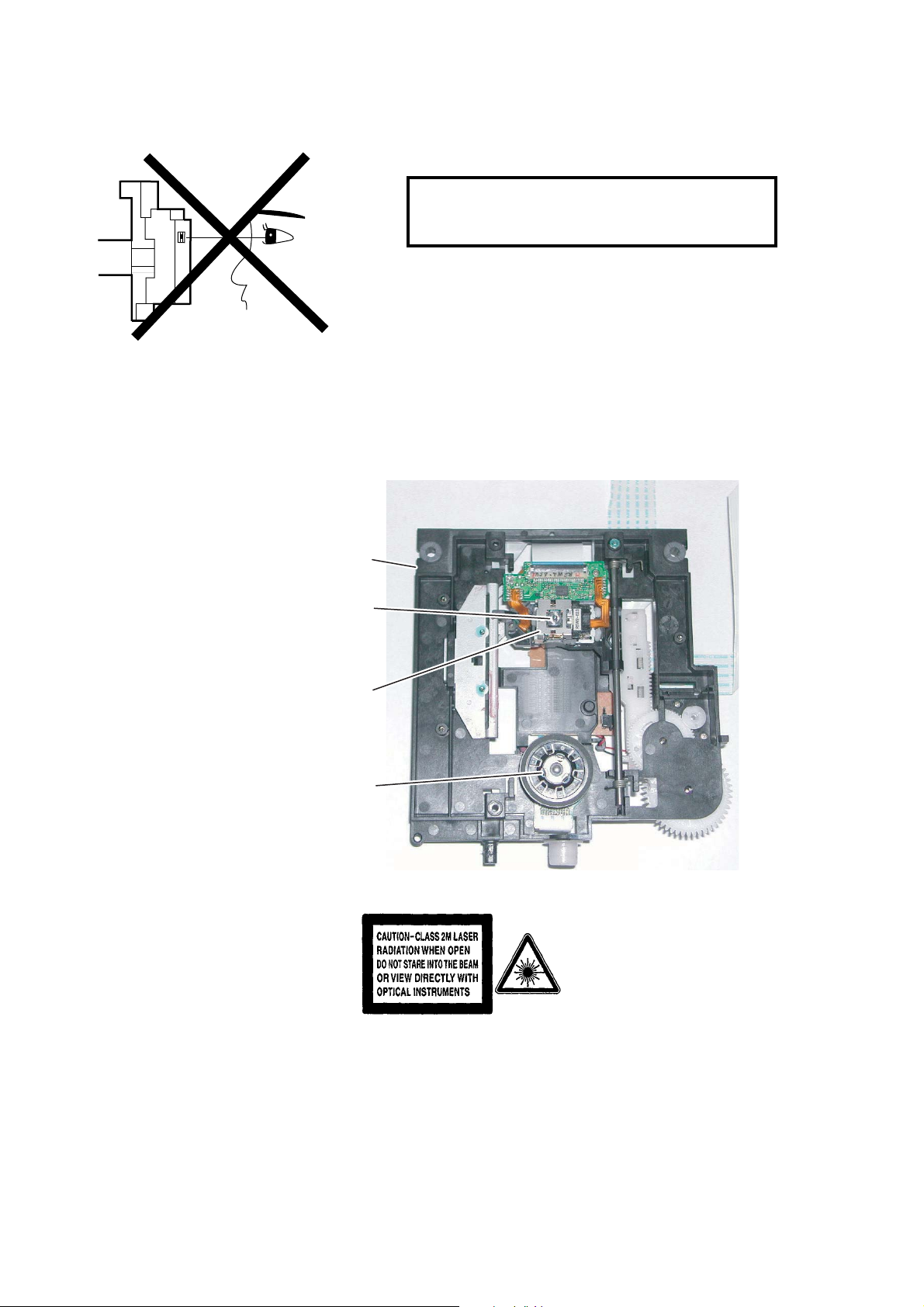
LASER BEAM SAFETY PRECAUTIONS
This DVD player uses a pickup that emits a laser beam.
Do not look directly at the laser beam coming
from the pickup or allow it to strike against your
skin.
The laser beam is emitted from the location shown in the figure. When checking the laser diode, be sure to keep
your eyes at least 30 cm away from the pickup lens when the diode is turned on. Do not look directly at the laser
beam.
CAUTION: Use of controls and adjustments, or doing procedures other than those specified herein, may result in
hazardous radiation exposure.
Drive Mechanism Assembly
Laser Beam Radiation
Laser Pickup
Turntable
Location: Inside Top of DVD mechanism.
1-2-1 TD5PLSP
Page 6

IMPORTANT SAFETY PRECAUTIONS
Product Safety Notice
Some electrical and mechanical parts have special
safety-related characteristics which are often not evident from visual inspection, nor can the protection
they give necessarily be obtained by replacing them
with components rated for higher voltage, wattage,
etc. Parts that have special safety characteristics are
identified by a ! on schematics and in parts lists. Use
of a substitute replacement that does not have the
same safety characteristics as the recommended
replacement part might create shock, fire, and/or other
hazards. The Product’s Safety is under review continuously and new instructions are issued whenever
appropriate. Prior to shipment from the factory, our
products are carefully inspected to confirm with the
recognized product safety and electrical codes of the
countries in which they are to be sold. However, in
order to maintain such compliance, it is equally important to implement the following precautions when a set
is being serviced.
Precautions during Servicing
A. Parts identified by the symbol are critical for
safety. Replace only with part number specified.
B. In addition to safety, other parts and assemblies
are specified for conformance with regulations
applying to spurious radiation. These must also be
replaced only with specified replacements.
Examples: RF converters, RF cables, noise blocking capacitors, and noise blocking filters, etc.
C. Use specified internal wiring. Note especially:
1)Wires covered with PVC tubing
2)Double insulated wires
3)High voltage leads
D. Use specified insulating materials for hazardous
live parts. Note especially:
1)Insulation tape
2)PVC tubing
3)Spacers
4)Insulators for transistors
E. When replacing AC primary side components
(transformers, power cord, etc.), wrap ends of
wires securely about the terminals before soldering.
F. Observe that the wires do not contact heat produc-
ing parts (heatsinks, oxide metal film resistors, fusible resistors, etc.).
G. Check that replaced wires do not contact sharp
edges or pointed parts.
H. When a power cord has been replaced, check that
5 - 6 kg of force in any direction will not loosen it.
I. Also check areas surrounding repaired locations.
J. Be careful that foreign objects (screws, solder
droplets, etc.) do not remain inside the set.
K. When connecting or disconnecting the internal
connectors, first, disconnect the AC plug from the
AC outlet.
L. Be sure to confirm the FAN motor has completely
stopped when disconnecting the AC cord for termination processing is activated during inner P-on
immediately after turning Power off.
1-3-1 DVDP_ISPT
Page 7
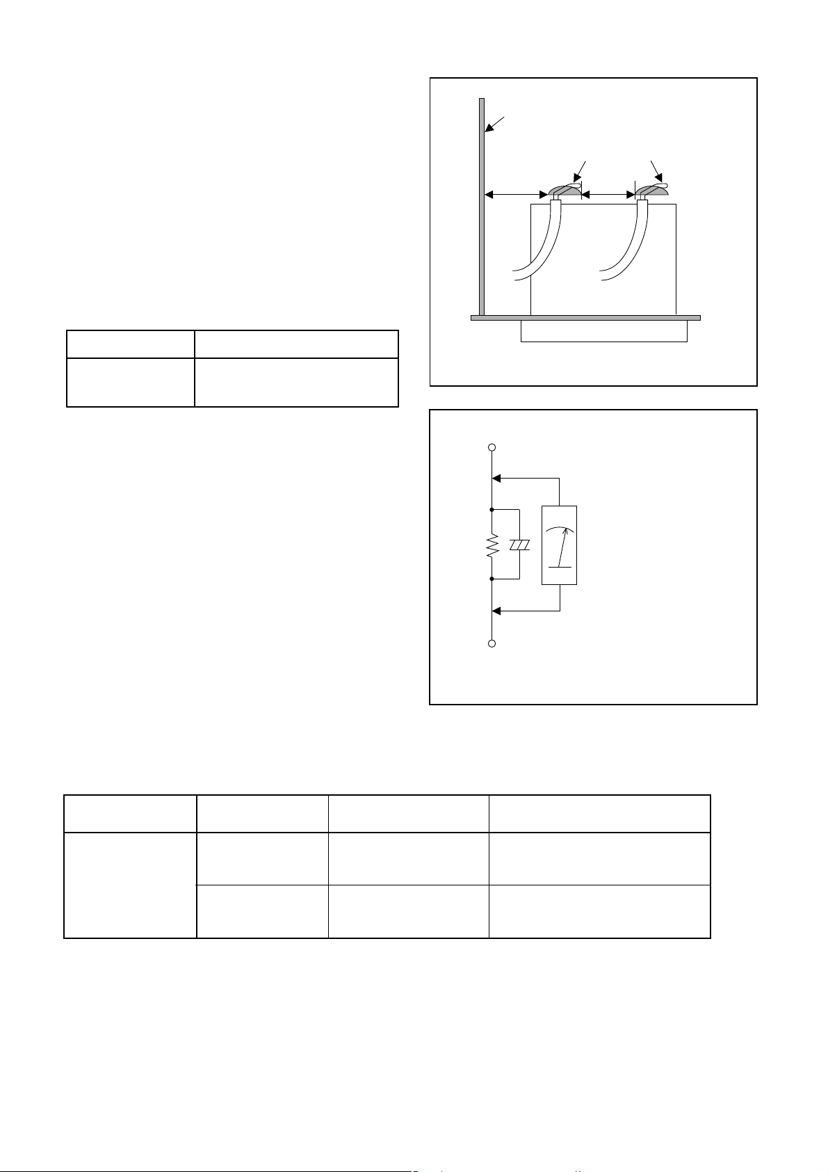
Safety Check after Servicing
Examine the area surrounding the repaired location
for damage or deterioration. Observe that screws,
parts, and wires have been returned to their original
positions. Afterwards, do the following tests and confirm the specified values to verify compliance with
safety standards.
1. Clearance Distance
When replacing primary circuit components, confirm
specified clearance distance (d) and (d’) between soldered terminals, and between terminals and surrounding metallic parts. (See Fig. 1)
Table 1 : Ratings for selected area
AC Line Voltage Clearance Distance (d), (d’)
230 V
Note: This table is unofficial and for reference only.
Be sure to confirm the precise values.
2. Leakage Current Test
≥ 3.2 mm(d)
≥ 6.0 mm(d’)
Chassis or Secondary Conductor
Primary Circuit
d' d
Fig. 1
Exposed Accessible Part
Confirm the specified (or lower) leakage current
between B (earth ground, power cord plug prongs)
and externally exposed accessible parts (RF terminals, antenna terminals, video and audio input and
output terminals, microphone jacks, earphone jacks,
etc.) is lower than or equal to the specified value in the
table below.
Measuring Method (Power ON) :
Insert load Z between B (earth ground, power cord
plug prongs) and exposed accessible parts. Use an
AC voltmeter to measure across the terminals of load
Z. See Fig. 2 and the following table.
Table 2: Leakage current ratings for selected areas
AC Line Voltage Load Z Leakage Current (i)
230 V
2kΩ RES.
Connected in
parallel
50kΩ RES.
Connected in
parallel
i≤0.7mA AC Peak
i≤2mA DC
i≤0.7mA AC Peak
i≤2mA DC
Z
One side of
B
Power Cord Plug Prongs
One side of power cord plug
AC Voltmeter
(High Impedance)
prongs (B) to:
RF or
Antenna terminals
A/V Input, Output
Fig. 2
Note: This table is unofficial and for reference only. Be sure to confirm the precise values.
1-3-2 DVDP_ISPT
Page 8

STANDARD NOTES FOR SERVICING
NOTE: BOARD MEANS PRINTED CIRCUIT BOARD.
Circuit Board Indications
1. The output pin of the 3 pin Regulator ICs is
indicated as shown.
Top View
Out
2. For other ICs, pin 1 and every fifth pin are
indicated as shown.
Pin 1
3. The 1st pin of every male connector is indicated as
shown.
Pin 1
Input
In
Bottom View
5
10
Pb (Lead) Free Solder
When soldering, be sure to use the Pb free solder.
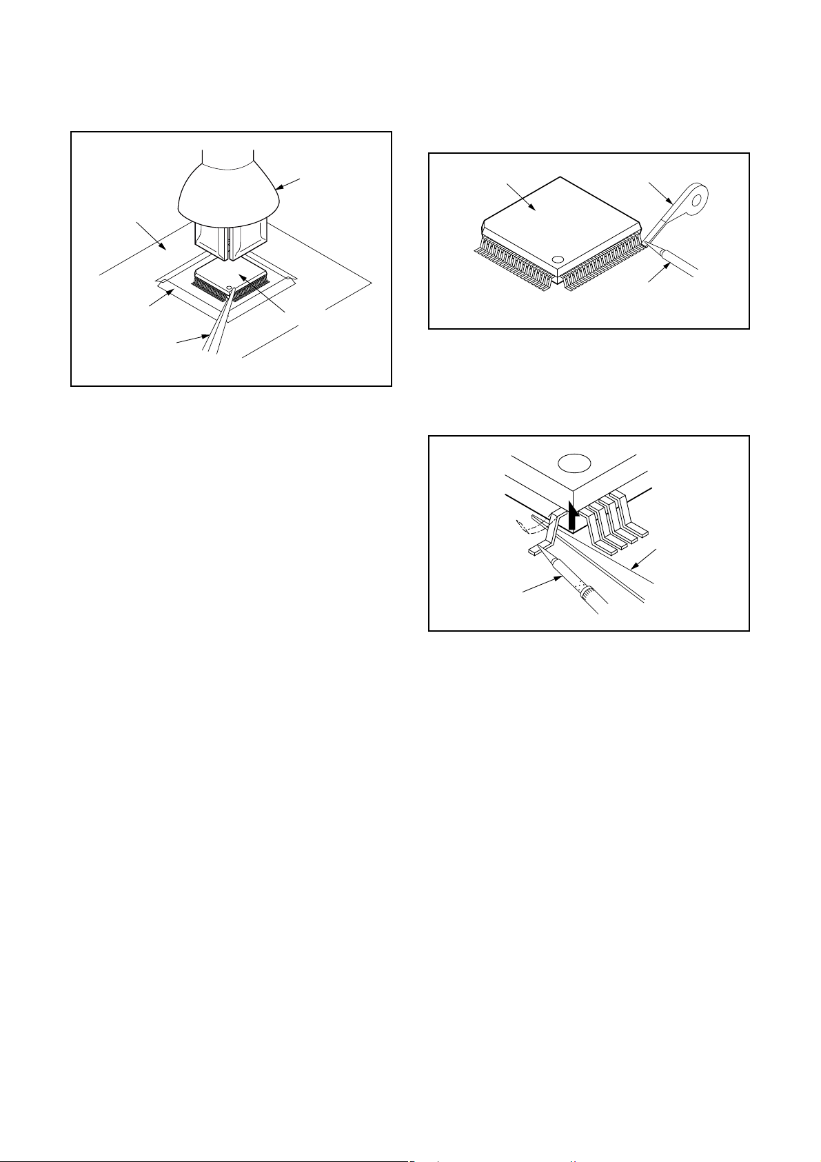
How to Remove / Install Flat Pack-IC
1. Removal
With Hot-Air Flat Pack-IC Desoldering Machine:
1. Prepare the hot-air flat pack-IC desoldering
machine, then apply hot air to the Flat Pack-IC
(about 5 to 6 seconds). (Fig. S-1-1)
Fig. S-1-1
Instructions for Connectors
1. When you connect or disconnect the FFC (Flexible
Foil Connector) cable, be sure to first disconnect
the AC cord.
2. FFC (Flexible Foil Connector) cable should be
inserted parallel into the connector, not at an
angle.
FFC Cable
Connector
BOARD
* Be careful to avoid a short circuit.
2. Remove the flat pack-IC with tweezers while
applying the hot air.
3. Bottom of the flat pack-IC is fixed with glue to the
BOARD; when removing entire flat pack-IC, first
apply soldering iron to center of the flat pack-IC
and heat up. Then remove (glue will be melted).
(Fig. S-1-6)
4. Release the flat pack-IC from the BOARD using
tweezers. (Fig. S-1-6)
CAUTION:
1. The Flat Pack-IC shape may differ by models. Use
an appropriate hot-air flat pack-IC desoldering
machine, whose shape matches that of the Flat
Pack-IC.
2. Do not supply hot air to the chip parts around the
flat pack-IC for over 6 seconds because damage
to the chip parts may occur. Put masking tape
around the flat pack-IC to protect other parts from
damage. (Fig. S-1-2)
1-4-1 DVDN_SN
Page 9
3. The flat pack-IC on the BOARD is affixed with
glue, so be careful not to break or damage the foil
of each pin or the solder lands under the IC when
removing it.
With Soldering Iron:
1. Using desoldering braid, remove the solder from
all pins of the flat pack-IC. When you use solder
flux which is applied to all pins of the flat pack-IC,
you can remove it easily. (Fig. S-1-3)
BOARD
Masking
Tape
Tweezers
Hot-air
Flat Pack-IC
Desoldering
Machine
Flat Pack-IC
Fig. S-1-2
Flat Pack-IC
Desoldering Braid
Soldering Iron
Fig. S-1-3
2. Lift each lead of the flat pack-IC upward one by
one, using a sharp pin or wire to which solder will
not adhere (iron wire). When heating the pins, use
a fine tip soldering iron or a hot air desoldering
machine. (Fig. S-1-4)
Sharp
Pin
Fine Tip
Soldering Iron
3. Bottom of the flat pack-IC is fixed with glue to the
BOARD; when removing entire flat pack-IC, first
apply soldering iron to center of the flat pack-IC
and heat up. Then remove (glue will be melted).
(Fig. S-1-6)
4. Release the flat pack-IC from the BOARD using
tweezers. (Fig. S-1-6)
Fig. S-1-4
1-4-2 DVDN_SN
Page 10
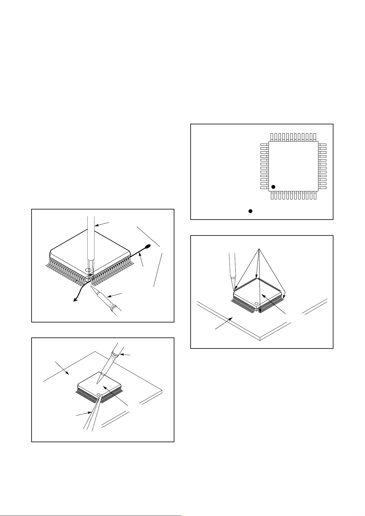
With Iron Wire:
1. Using desoldering braid, remove the solder from
all pins of the flat pack-IC. When you use solder
flux which is applied to all pins of the flat pack-IC,
you can remove it easily. (Fig. S-1-3)
2. Affix the wire to a workbench or solid mounting
point, as shown in Fig. S-1-5.
3. While heating the pins using a fine tip soldering
iron or hot air blower, pull up the wire as the solder
melts so as to lift the IC leads from the BOARD
contact pads as shown in Fig. S-1-5.
4. Bottom of the flat pack-IC is fixed with glue to the
BOARD; when removing entire flat pack-IC, first
apply soldering iron to center of the flat pack-IC
and heat up. Then remove (glue will be melted).
(Fig. S-1-6)
5. Release the flat pack-IC from the BOARD using
tweezers. (Fig. S-1-6)
Note: When using a soldering iron, care must be
taken to ensure that the flat pack-IC is not
being held by glue. When the flat pack-IC is
removed from the BOARD, handle it gently
because it may be damaged if force is applied.
Hot Air Blower
2. Installation
1. Using desoldering braid, remove the solder from
the foil of each pin of the flat pack-IC on the
BOARD so you can install a replacement flat packIC more easily.
2. The “●” mark on the flat pack-IC indicates pin 1.
(See Fig. S-1-7.) Be sure this mark matches the 1
on the BOARD when positioning for installation.
Then presolder the four corners of the flat pack-IC.
(See Fig. S-1-8.)
3. Solder all pins of the flat pack-IC. Be sure that
none of the pins have solder bridges.
Example :
Pin 1 of the Flat Pack-IC
is indicated by a " " mark.
Fig. S-1-7
To Solid
Mounting Point
BOARD
Tweezers
Iron Wire
Soldering Iron
Fig. S-1-5
Fine Tip
Soldering Iron
Flat Pack-IC
or
Presolder
Flat Pack-IC
BOARD
Fig. S-1-8
Fig. S-1-6
1-4-3 DVDN_SN
Page 11
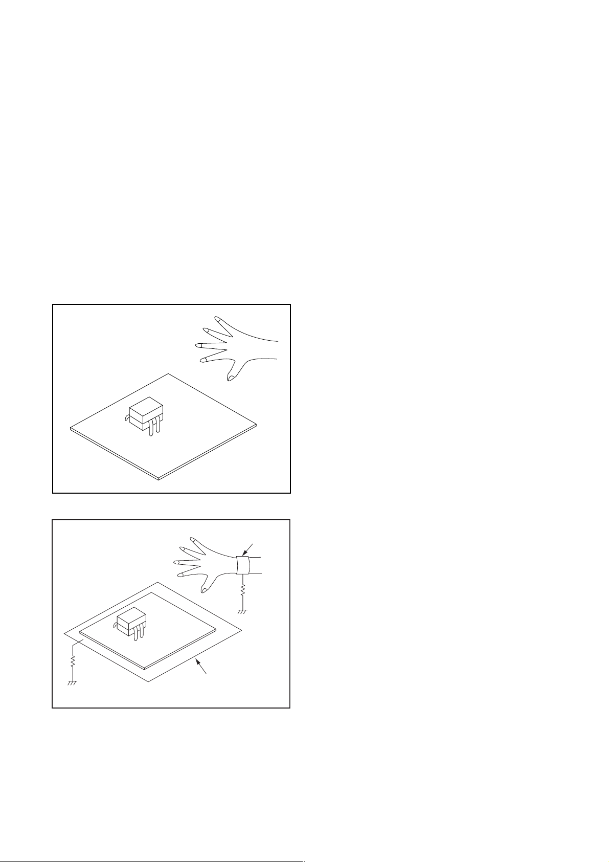
Instructions for Handling Semiconductors
Electrostatic breakdown of the semi-conductors may
occur due to a potential difference caused by
electrostatic charge during unpacking or repair work.
1. Ground for Human Body
Be sure to wear a grounding band (1 MΩ) that is
properly grounded to remove any static electricity that
may be charged on the body.
2. Ground for Workbench
Be sure to place a conductive sheet or copper plate
with proper grounding (1 MΩ) on the workbench or
other surface, where the semi-conductors are to be
placed. Because the static electricity charge on
clothing will not escape through the body grounding
band, be careful to avoid contacting semi-conductors
with your clothing.
<Incorrect>
<Correct>
1MΩ
BOARD
Grounding Band
1MΩ
BOARD
Conductive Sheet or
Copper Plate
1-4-4 DVDN_SN
Page 12
HANDLING PRECAUTIONS FOR HDD
CAUTION:
1. SHOCK
a. Exposing HDD to shock may be the biggest
damaging factor. Please note that HDD is easily
damaged even if dropped from any height. Be sure
to place HDD on a shock-absorbent mat. Also, be
careful when transporting HDD.
b. Be careful not to subject HDD to any shock when
tightening screws for HDD replacement.
(Tighten screws manually, not with an electric
driver.)
2. MOISTURE
a. Moisture may also be a damaging factor. HDD is
semiclosed style. Sudden changes in ambient
temperature may cause moisture to form. Monitor
temperature and do not allow moisture to form on
the media surface. Also, when opening HDD
package, do so only after package is at ambient
temperature.
b. After replacing HDD, leave it to reach room
temperature (about 2 hours) for preventing dew
internal condensation, and then work necessary
task such as operation check.
4. OTHERS
a. Be careful so as not to do the followings.
Otherwise, HDD might be damaged.
- DO NOT disassemble HDD.
- When handling HDD, be sure to hold both sides
securely.
b. HDD should be stored, packed in the protective
bag, in suitable surroundings (i.e., no extreme
changes in temperature to avoid condensation).
c. When transporting HDD, be sure to use the
exclusive packing case (the replacement HDD
carton).
d. Do not stack HDDs.
e. Do not place vertically because HDD is unstable
and easy to fall.
3. STATIC ELECTRICITY
a. After removing HDD or taking replacement HDD
out of the protective bag (the replacement HDD is
packed in a protective bag), place HDD on a
conductive surface. A grounding band should be
worn when handling.
Grounding Band
Both the conductive surface and grounding band
should be grounded.
b. Make sure that HDD is placed on main unit
completely and then let go of it, when assembling.
c. Do not put HDD on a packing bag. (for preventing
electrostatic damage)
1-5-1 DHD_SN
Page 13
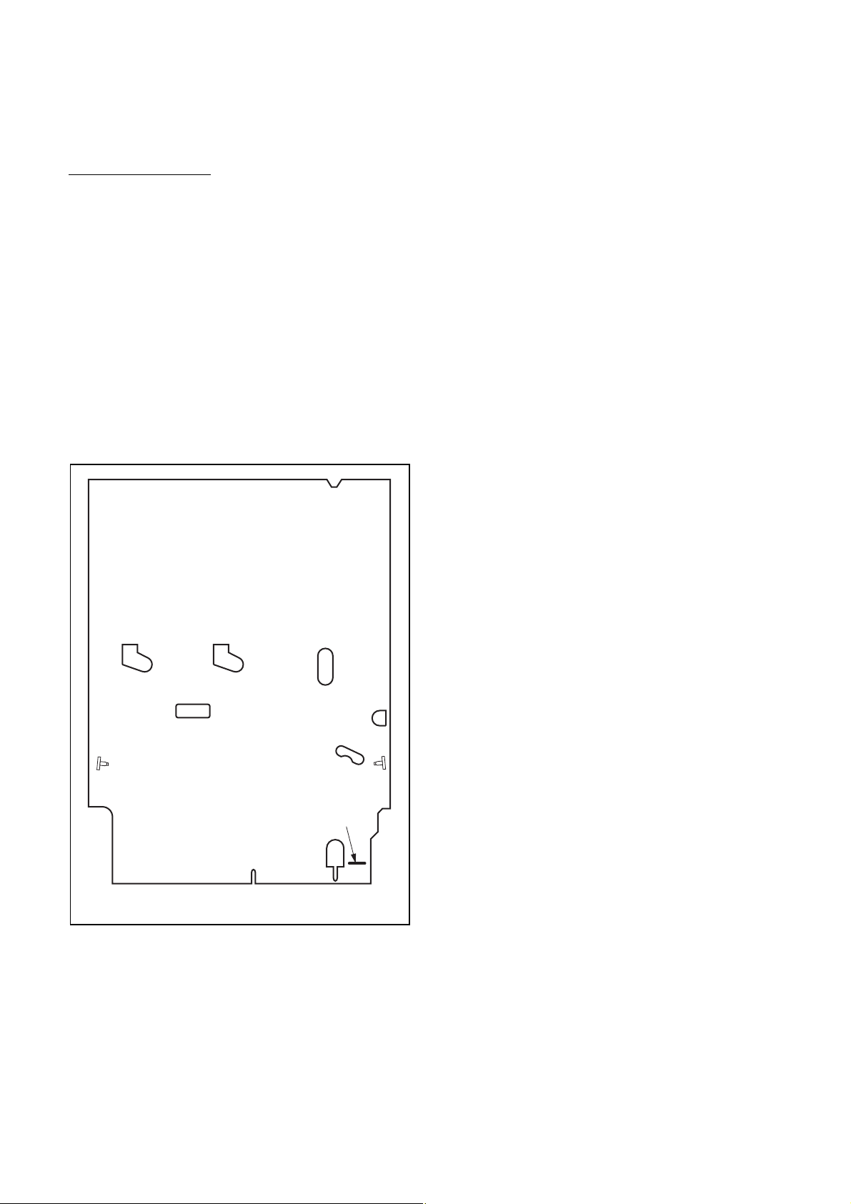
PREPARATION FOR SERVICING
How to Enter the Service Mode
About Optical Sensors
Caution:
An optical sensor system is used for the Tape Start
and End Sensors on this equipment. Carefully read
and follow the instructions below. Otherwise the unit
may operate erratically.
What to do for preparation
Insert a tape into the Deck Mechanism Assembly and
press [VCR PLAY] button. The tape will be loaded into
the Deck Mechanism Assembly. Make sure the power
is on, connect J917 (S-INH) to GND. This will stop the
function of Tape Start Sensor, Tape End Sensor and
Reel Sensors. (If these TPs are connected before
plugging in the unit, the function of the sensors will
stay valid.) See Fig. 1.
Q503
J917 (S-INH)
Note: Because the Tape End Sensors are inactive, do
not run a tape all the way to the start or the end of the
tape to avoid tape damage.
Q504
Fig. 1
1-6-1 E3NG0PFS
Page 14
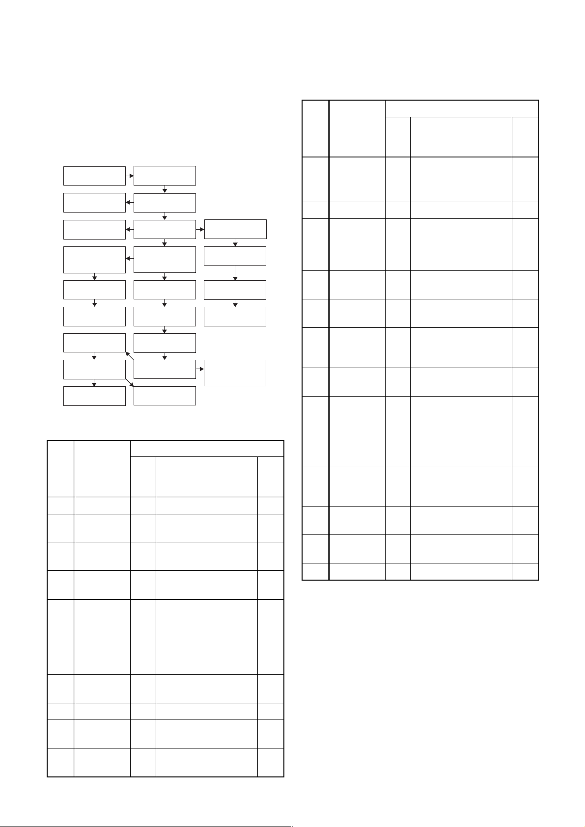
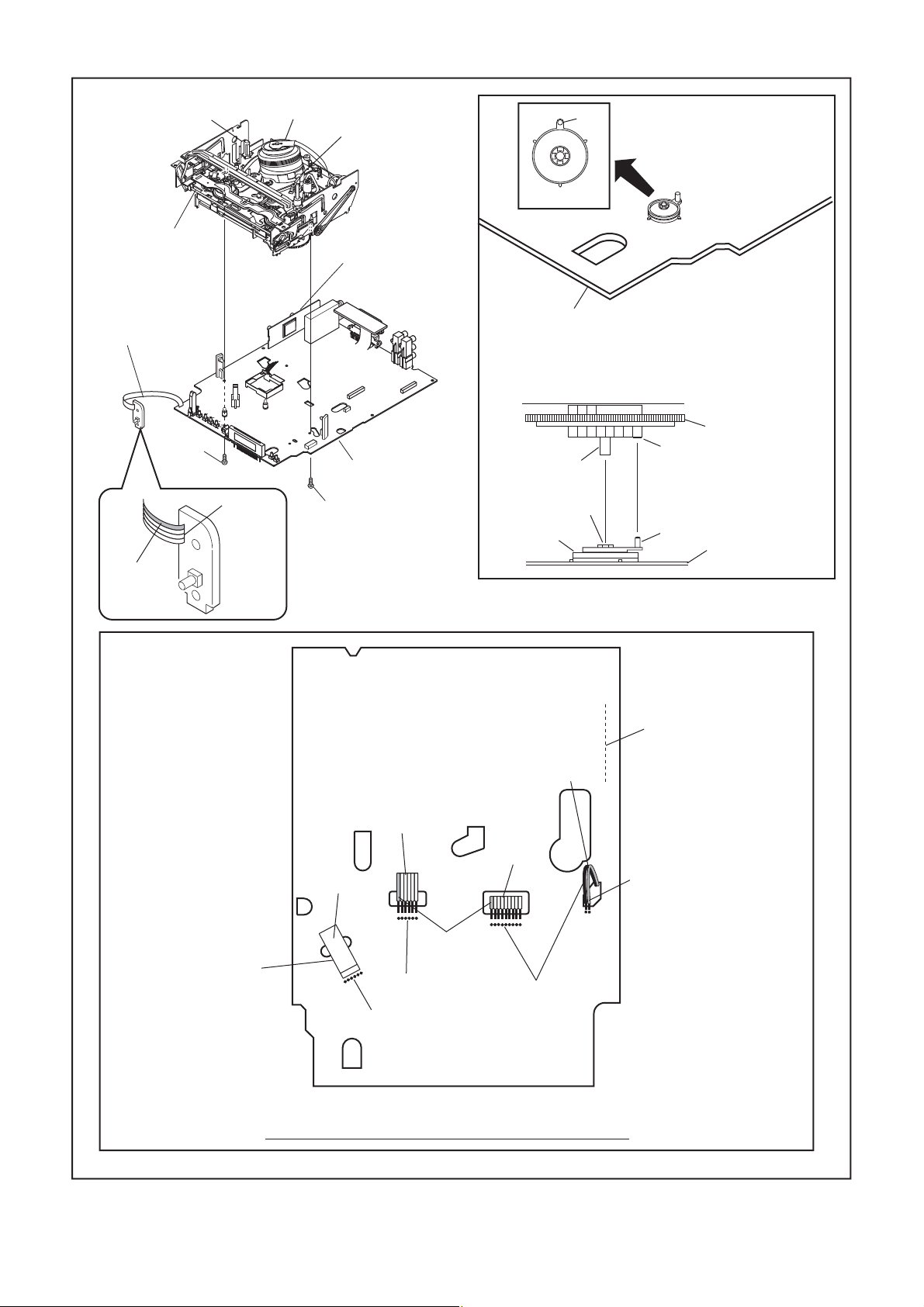
CABINET DISASSEMBLY INSTRUCTIONS
NOTE: BOARD MEANS PRINTED CIRCUIT BOARD.
1. Disassembly Flowchart
This flowchart indicates the disassembly steps to gain
access to item(s) to be serviced. When reassembling,
follow the steps in reverse order. Bend, route, and
dress the cables as they were originally.
[1] Cover Top
[22] Front
Bracket R
[23] Bracket R
[13] BOARD
Power
Supply
[14] BOARD
Switch
[15] BOARD
Front Jack
[17] Deck
Assembly
[18] BOARD
AV
[19] BOARD
DTV Module Unit
[2] Front
Assembly
[3] Front
Bracket
[4] HDD
Assembly
[5] DVD Mechanism
& DVD/HDD MAIN
BOARD Assembly
[10] Fan Holder
[11] Motor DC
Fan
[12] Panel Rear
[16] VCR
Chassis Unit
[21] Deck
Pedestal
[6] HDD
Bracket
[7] HDD Unit
[8] HDD
Support
[9] BOARD ATA
[20] BOARD
Power
Switch
ID/
LOC.
No.
PART
REMOVE/*UNHOOK/
Fig.
UNLOCK/RELEASE/
No.
UNPLUG/DESOLDER
Note
[10] Fan Holder D5 2(S-14), *CN1002 ---
REMOVAL
Motor DC
[11]
Fan
D5 2(S-15) ---
[12] Panel Rear D5 (S-16), 3(S-17) ---
(S-18), 3(S-19),
(S-20), *CN1503, FFC
D6
Guide, Chassis Earth
Plate
D6 (S-21), Desolder ---
D6 2(S-22), *CN3011 ---
5(S-23), 4(S-24),
D7
(S-25)
(S-26), (S-27),
D8
Desolder
[13]
[14]
[15]
[16]
[17]
BOARD
Power
Supply
BOARD
Switch
BOARD
Front Jack
VCR
Chassis
Unit
Deck
Assembly
[18] BOARD AV D8 ---------- ---
---
---
3
4
2. Disassembly Method
ID/
LOC.
No.
PART
Fig.
No.
[1] Cover Top D1 7(S-1) ---
Front
[2]
[3]
[4]
Assembly
Front
Bracket
HDD
Assembly
D2 (S-2), *5(L-1), *3(L-2) 1
D2
D3
DVD
Mechanism
[5]
& DVD/
HDD MAIN
D3
BOARD
Assembly
HDD
[6]
Bracket
D4 4(S-12) ---
[7] HDD Unit D4 4(S-13), HDD Rubber 2
HDD
[8]
[9]
Support
BOARD
ATA
D4 ---------- ---
D4 *CN3001, *CN3002 ---
REMOVAL
REMOVE/*UNHOOK/
UNLOCK/RELEASE/
UNPLUG/DESOLDER
(S-3), 3(S-4), Front
Support
(S-5), 3(S-6), *CN652,
Connector
(S-7), 2(S-8), 2(S-9),
2(S-10), *CN101,
*CN502-D, *CN701,
*CN901, Dust Cover,
Hook, Mecha Plate
Earth
Note
---
---
2
BOARD
DTV
[19]
Module
D8 Desolder ---
Unit
BOARD
[20]
Power
D8 Desolder ---
Switch
Deck
[21]
[22]
Pedestal
Front
Bracket R
D9 7(S-28) ---
(S-29), 2(S-30), DV
D9
Cable, DV Plate Earth
---
[23] Bracket R D9 2(S-31) ---
↓
(1)
↓
(2)
↓
(3)
↓
(4)
(5)
Note:
(1): Identification (location) No. of parts in the figures
(2): Name of the part
(3): Figure Number for reference
(4): Identification of parts to be removed, unhooked,
unlocked, released, unplugged, unclamped, or
desoldered.
P=Spring, L=Locking Tab, S=Screw,
CN=Connector
*=Unhook, Unlock, Release, Unplug, or Desolder
e.g. 6(S-1) = six Screws (S-1),
5(L-1) = five Locking Tabs (L-1)
(5): Refer to “Reference Notes.”
↓
1-7-1 E3NG1DC
Page 15
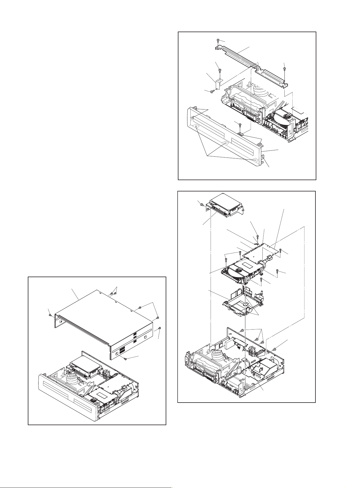
Reference Notes
1. Locking Tabs (L-1) and (L-2) are fragile. Be careful
not to break them.
1-1. Remove Screw (S-2).
1-2. Release five Locking Tabs (L-1).
1-3. Release three Locking Tabs (L-2) and
remove the Front Assembly.
2. Do not replace the DVD Mechanism or the DVD/
HDD MAIN BOARD Assembly separately, when
replacing the DVD Mechanism & DVD/HDD MAIN
BOARD Assembly. Order the new DVD
Mechanism & DVD/HDD MAIN BOARD Assembly.
2-1. Whenever you have replaced the HDD unit,
initialize the HDD unit. To initialize the HDD
unit, perform the following.To put the HDD &
DVD/VCR into the HDD mode, press the
[HDD] button on the remote control unit.
2-2. To put the HDD & DVD/VCR into the self-
check mode, after pressing [VARIABLE
SKIP] button, press the [3], [6], and [9]
buttons on the remote control in that order
within three seconds.
2-3. Press [ENTER] button. The HDD & DVD/
VCR is initialized and the power is turned off
automatically after two seconds.
3. When reassembling, solder wire jumpers as
shown in Fig. D8.
4. Before installing the Deck Assembly, be sure to
place the pin of LD-SW on the BOARD AV as
shown in Fig. D8. Then, install the Deck Assembly
while aligning the hole of Cam Gear with the pin of
LD-SW, the shaft of Cam Gear with the hole of LDSW as shown in Fig. D8.
Front
Support
(S-4)
(L-2)
(S-5)
[4] HDD
Assembly
CN901
(S-4)
(L-1)
(S-2)
Mecha Plate
Earth
CN101
(S-10)
(S-4)
[3] Front Bracket
(S-3)
(L-1)
[2] Front
Assembly
(L-1)
Fig. D2
[5] DVD Mechanism &
DVD/HDD MAIN BOARD
Assembly
(S-8)
CN502-D
CN652
CN701
(S-8)
(S-9)
[1] Cover Top
(S-1)
(S-1)
(S-1)
Fig. D1
(S-1)
(S-1)
Dust Cover
(S-9)
Hook
(S-6)
Connector
(S-7)
Fig. D3
1-7-2 E3NG1DC
Page 16
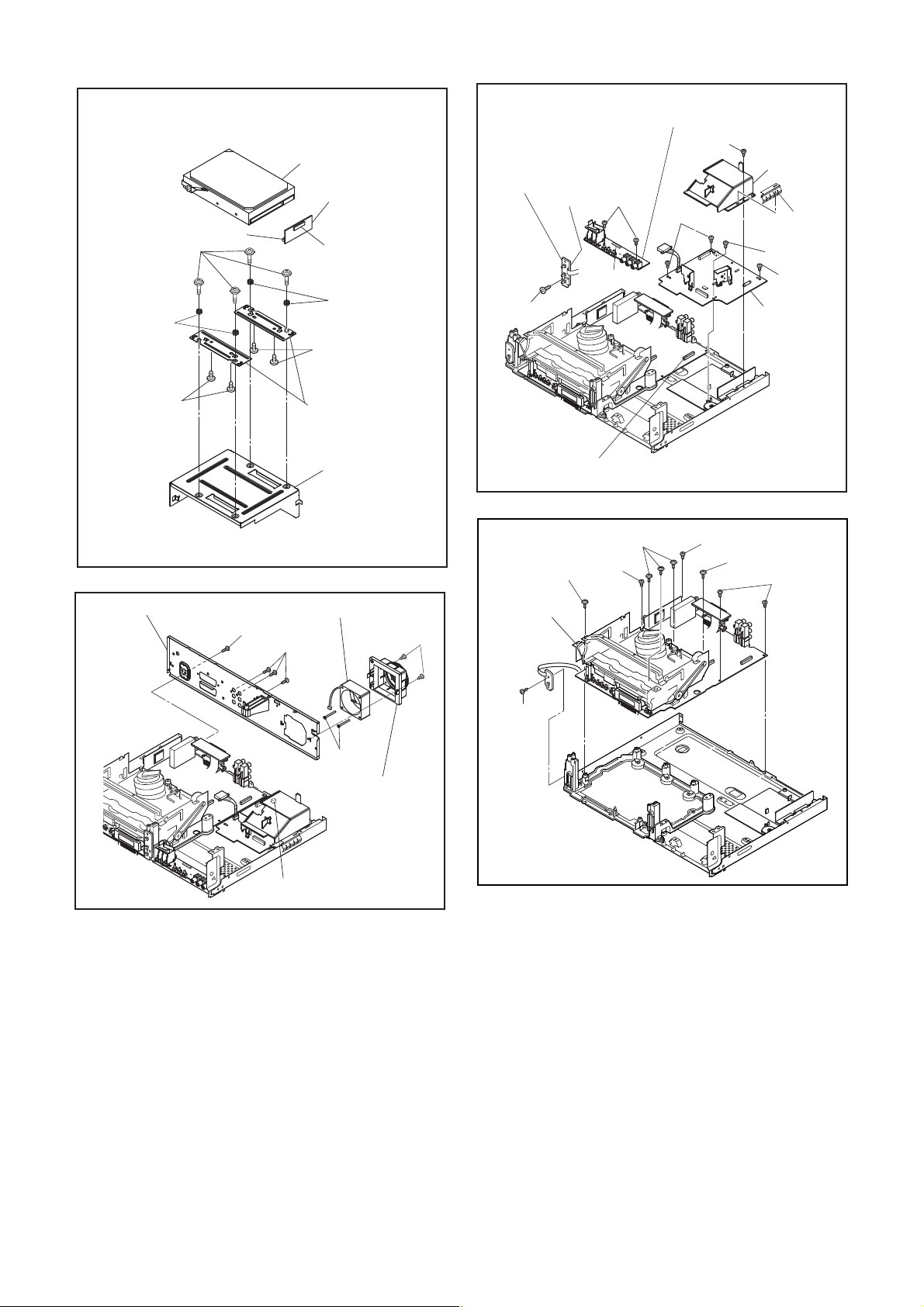
HDD Rubber
(S-12)
CN3001
[7] HDD Unit
[9] BOARD ATA
CN3002
HDD Rubber
(S-13)
[14] BOARD
Switch
Desolder
(S-21)
[15] BOARD Front Jack
(S-18)
(S-22)
(S-19)
CN3011
FFC Guide
Chassis
Earth Plate
(S-20)
(S-19)
[13] BOARD
Power
Supply
(S-13)
[12] Rear Panel
[8] HDD Support
[6] HDD Bracket
[11] Motor DC Fan
(S-16)
(S-17)
Fig. D4
(S-14)
(S-15)
[10] Fan Holder
(S-23)
[16] VCR
Chassis
Unit
(S-25)
CN1503
(S-23)
(S-24)
Fig. D6
(S-24)
(S-23)
(S-24)
CN1002
Fig. D7
Fig. D5
1-7-3 E3NG1DC
Page 17
FE Head
[17] Deck
Assembly
Cylinder
Assembly
ACE Head
Assembly
[19]
BOARD DTV
Module Unit
Pin
Pin
SW507
LD-SW
[20] BOARD
Power Switch
(S-26)
Lead with
blue stripe
Desolder
[18] BOARD AV
(S-27)
From
ACE Head
Assembly
Printing side
[18] BOARD AV
[17] Deck Assembly
Shaft
Hole
LD-SW
From
FE Head
From
Cylinder
Assembly
Cam Gear
Hole
Pin
[18] BOARD AV
Desolder
Lead with
gray stripe
From
Capstan
Motor
Assembly
Lead with
blue stripe
Desolder
Desolder
Desolder
BOTTOM VIEW
Lead connections of Deck Assembly and BOARD AV
1-7-4 E3NG1DC
Fig. D8
Page 18
(S-28)
DV PlateEarth
(S-28)
[21] Deck Pedestal
[22] Front Bracket R
[23] Bracket R
(S-31)
(S-30)
DV Cable
(S-29)
Fig. D9
3. How to Eject Manually
Note: When rotating the gear, be careful not to damage the gear.
1. Remove the Cover Top, Front Assembly, Front Bracket, DVD Mechanism & DVD/HDD MAIN BOARD
Assembly.
2. Remove the Dust Cover.
3. Rotate the gear in the direction of the arrow manually as shown below.
View for A
A
Rotate this gear in
Hook
the direction of the arrow
1-7-5 E3NG1DC
Page 19
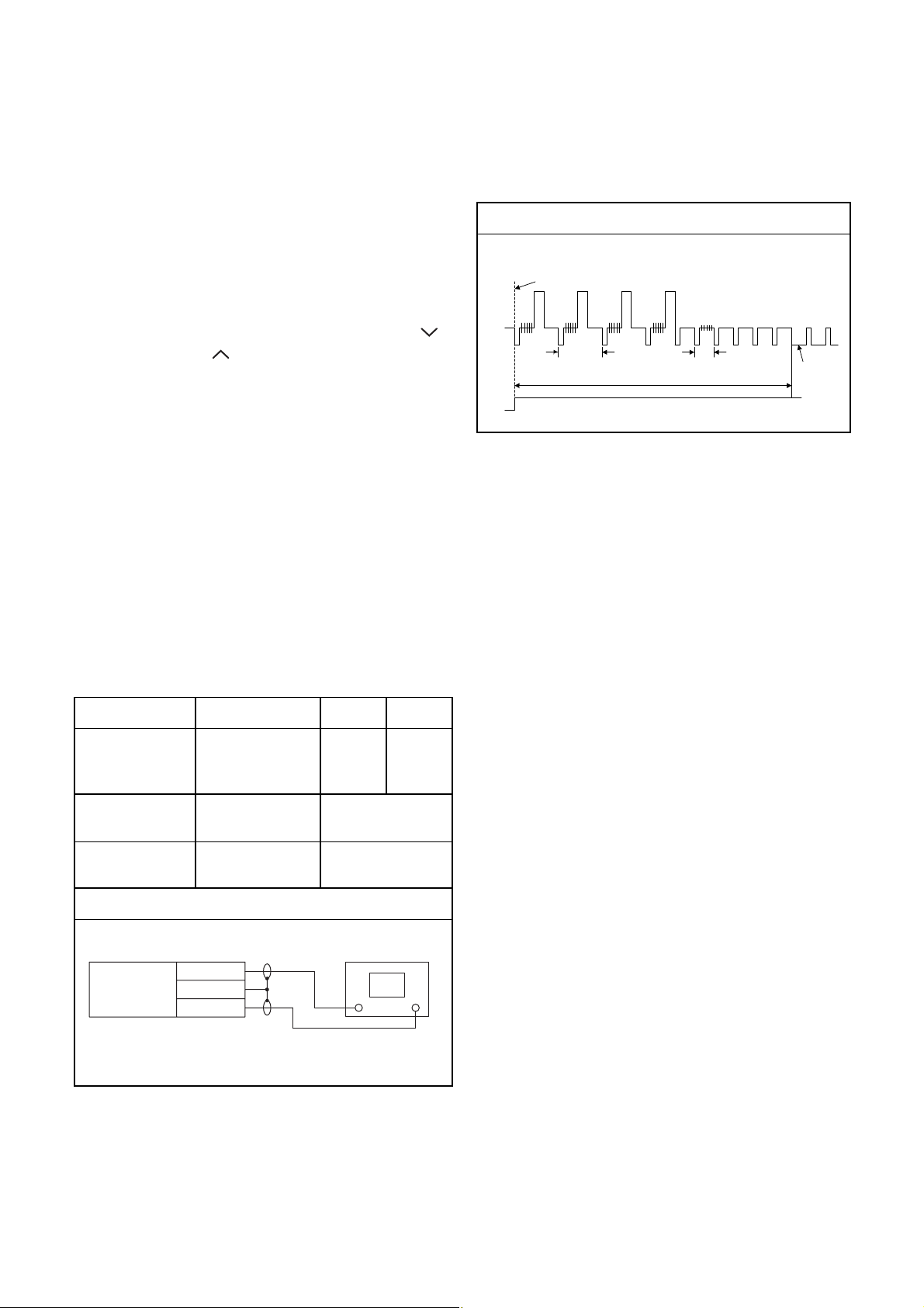
ELECTRICAL ADJUSTMENT INSTRUCTIONS
NOTE: BOARD MEANS PRINTED CIRCUIT BOARD.
NOTE:
1.Electrical adjustments are required after replacing
circuit components and certain mechanical parts.
It is important to do these adjustments only after
all repairs and replacements have been completed. Also, do not attempt these adjustments
unless the proper equipment is available.
2.To perform these alignment / confirmation procedures, make sure that the tracking control is set in
the center position: Press either [PROGRAM 5??]
or [PROGRAM ] button on the front panel first,
then the [ O ] (VCR) button on the front panel.
CH1
CH2
Figure 1
EXT. Syncronize Trigger Point
1.0H
6.5H±1H (416 μs ± 64 μs)
0.5H
V-Sync
Test Equipment Required
1.Oscilloscope: Dual-trace with 10:1 probe,
V-Range: 0.001~50V/Div.,
F-Range: DC~AC-20MHz
2.Alignment Tape (FL6A)
Head Switching Position Adjustment
Purpose:
To determine the Head Switching position during
playback.
Symptom of Misadjustment:
May cause Head Switching noise or vertical jitter
in the picture.
Test point Adj.Point Mode Input
J184(
AV1-V-OUT1
TP504(RF-SW)
GND
Tape
FL6A Oscilloscope
)
VR501
(Switching Point)
(BOARD AV)
Measurement
Equipment
PLAY
(SP)
6.5H±1H
(416μs±64μs)
-----
Spec.
Switching Pulse
Reference Notes:
Playback the Alignment tape and adjust VR501 so that
the V-sync front edge of the CH1 video output waveform is at the 6.5H±1H (416μs±64μs) delayed position
from the rising edge of the CH2 head switching pulse
waveform.
Connections of Measurement Equipment
Oscilloscope
BOARD
AV
J184
GND
TP504
CH1 CH2
Trig. (+)
1-8-1 E3NG0EA
Page 20
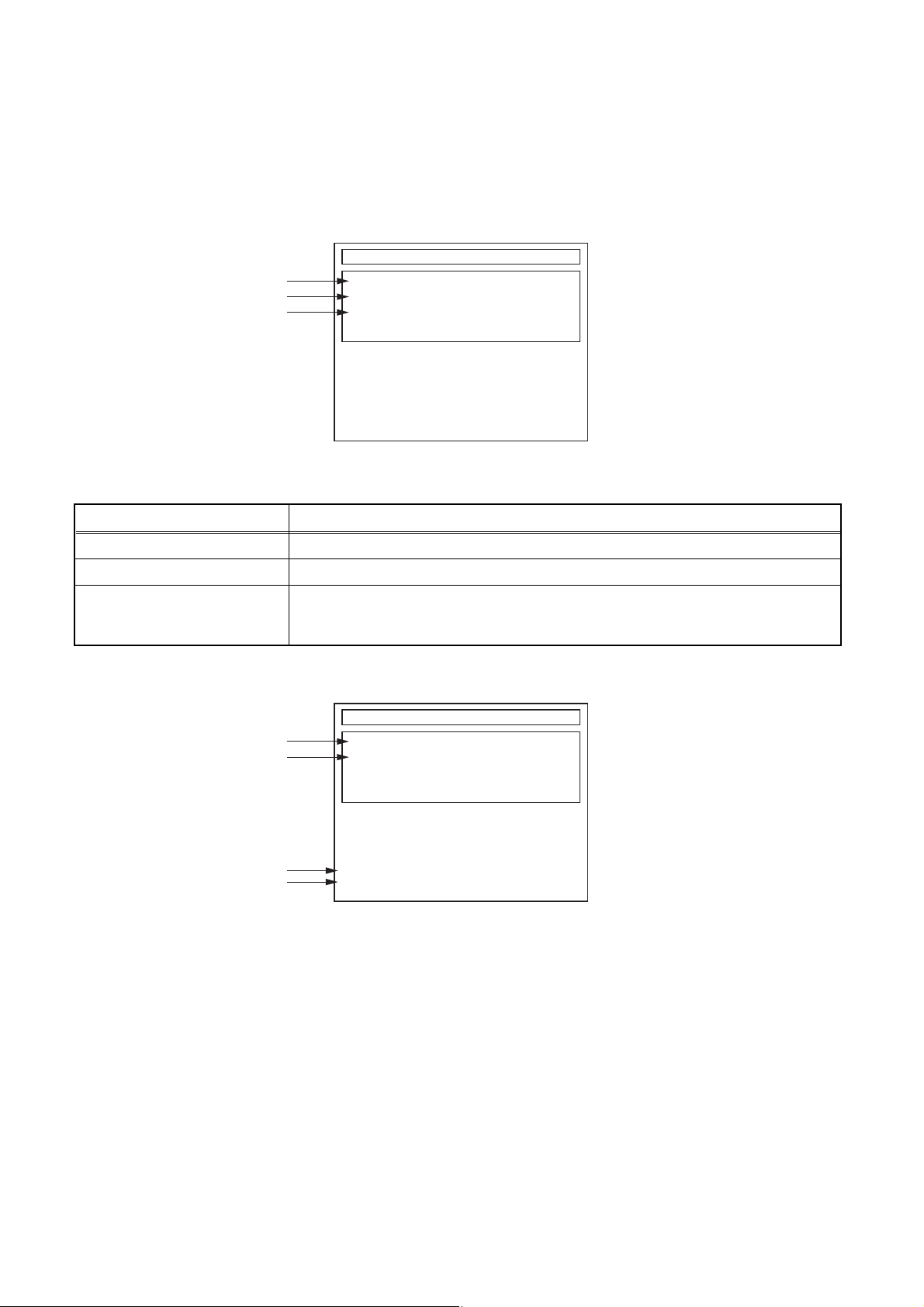
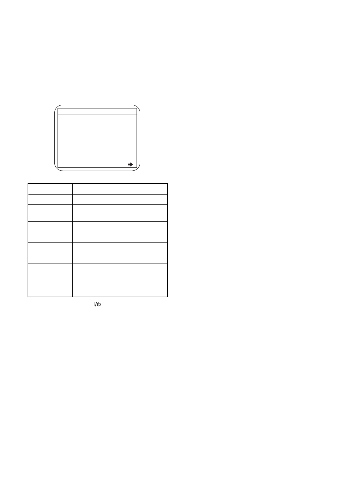
HOW TO SELF-CHECK AND INITIALIZE THE HDD & DVD/VCR
1. Turn on the HDD & DVD/VCR.
2. To put the HDD & DVD/VCR into the HDD mode, press [HDD] on the remote control unit.
3. To put the HDD & DVD/VCR into the self-check mode, after pressing [VARIABLE SKIP] button, press the [0],
[7], and [9] buttons on the remote control in that order within three seconds.
Fig. a appears on the screen and all LEDs light.
SELF CHECK
*1
*2
*3
DVD CONNECT STATUS :
HDD CONNECT STATUS :
HDD POWER ON HOURS :
HDD FORMAT START :
POWER OFF :
ENTER
POWER
Fig. a: Self-Check Mode Screen
Table 1: Description of Fig. a
INDICATION DESCRIPTION
DVD CONNECT STATUS (*1) Connecting Condition of DVD(F/E)
HDD CONNECT STATUS (*2) Connecting Condition of HDD
Value of HDD power on hours obtained from S.M.A.R.T. command. (If not obtainable,
HDD POWER ON HOURS (*3)
value of HDD power on hours is “0”.)
Value in parentheses is the factory setting value. (If no setting, the value is “0”.)
4. Upon the self-check completion, Fig. b appears on the screen.
SELF CHECK
*4
*5
DVD CONNECT STATUS : OK
HDD CONNECT STATUS : OK
HDD POWER ON HOURS : 70
*6
*7
HDD FORMAT START :
POWER OFF :
ENTER
POWER
Fig. b: Screen of Finishing Self-Check Mode
1-9-1 E3NG0INT
Page 21
Table 2: Indication of DVD self-check (*4)
INDICATION DESCRIPTION
OK Connection of DVD is normal.
NOT FOUND DVD drive cannot be found.
CABLE ERROR
FFC cable (connecting to CN652) between the DVD drive and the DVD/HDD MAIN BOARD
is not connected correctly.
Table 3: Indication of HDD self-check (*5)
INDICATION DESCRIPTION
OK Connection of HDD is normal.
NOT FOUND HDD drive cannot be found.
CABLE ERROR FFC cable between the BOARD ATA and the HDD drive is not connected correctly.
Table 4: Available button in self-check mode
BUTTON DESCRIPTION
ENTER (*6) Initialize (only when the self-check mode is complete)
ON / STANDBY (*7) Turn the power off
OTHER Not available
5. When the self-check mode is complete, press [ ] button to turn the power off.
When initializing the HDD & DVD/VCR, press [ENTER] button.After two seconds, the power is turned off
automatically.
NOTE: When initializing, “Current Clock” and “HDD Contents” are initialized.
1-9-2 E3NG0INT
Page 22

HOW TO INITIALIZE THE HDD & DVD/VCR
To put the program back at the factory-default, initialize the DVD recorder & VCR as the following procedure.
< HDD/DVD Section >
1. Turn on the HDD & DVD/VCR.
2. To put the HDD & DVD/VCR into the HDD mode, press [HDD] on the remote control unit.
3. To put the HDD & DVD/VCR into the Version display mode, press [VARIABLE SKIP], [1], [2], and [3] buttons
on the remote control unit in that order within three seconds.
Fig. a appears on the screen.
*1: "
*2: Firmware Version differs depending on the
models, and this indication is one example.
Fig. a Version Display Mode Screen
" differs depending on the models.
*******
F/W VERSION DISP
MODEL NAME :
DVB-T VERSION :
FE VERSION :
BE VERSION :
TT VERSION :
DV UNIQUE ID :
LD ADJUSTMENT :
DISC ADJUSTMENT :
DEFAULT SETTING : ENTER
EXIT : RETURN
*******
*.**
***_***_***
************
*********
******** ********
OK
OK
4. Press [ENTER] button, then the HDD & DVD/VCR starts initializing. When the initializing is completed, the
HDD & DVD/VCR exits the Version display mode and turns off the power automatically.
* To move into the Normal mode from the Version display mode, press [RETURN] button on the remote
control unit instead of [ENTER] button.
* When [ ] button is pressed before [ENTER] button is pressed, the HDD & DVD/VCR exits the Version
display mode, then the power turns off.
NOTE: When initializing, “Current Clock”, “Setup Changing Item”, “Channel Setup”, “Area Setup” and “Program”
are initialized.
1-9-3 E3NG0INT
Page 23
FIRMWARE RENEWAL MODE
1. Turn the power on and remove the disc in the tray.
2. To switch the HDD & DVD into the HDD mode,
press [HDD] on the remote control unit.
3. To put the HDD & DVD into version up mode,
press [VARIABLE SKIP] and [6], [5], [4] buttons on
the remote control unit in that order within 3
seconds. The tray will open automatically.
Fig. a appears on the TV screen and Fig. b
appears on the VFD.
*FIRMWARE version will differ depending on the
model. Fig. a is an example.
Firm Update Mode ver.TD5******X2G
Please insert a disc.
Fig. a: Update Mode TV Screen
5. Select the firmware version pressing arrow
buttons, then press [ENTER].
Fig. d appears on the screen and Fig. e appears
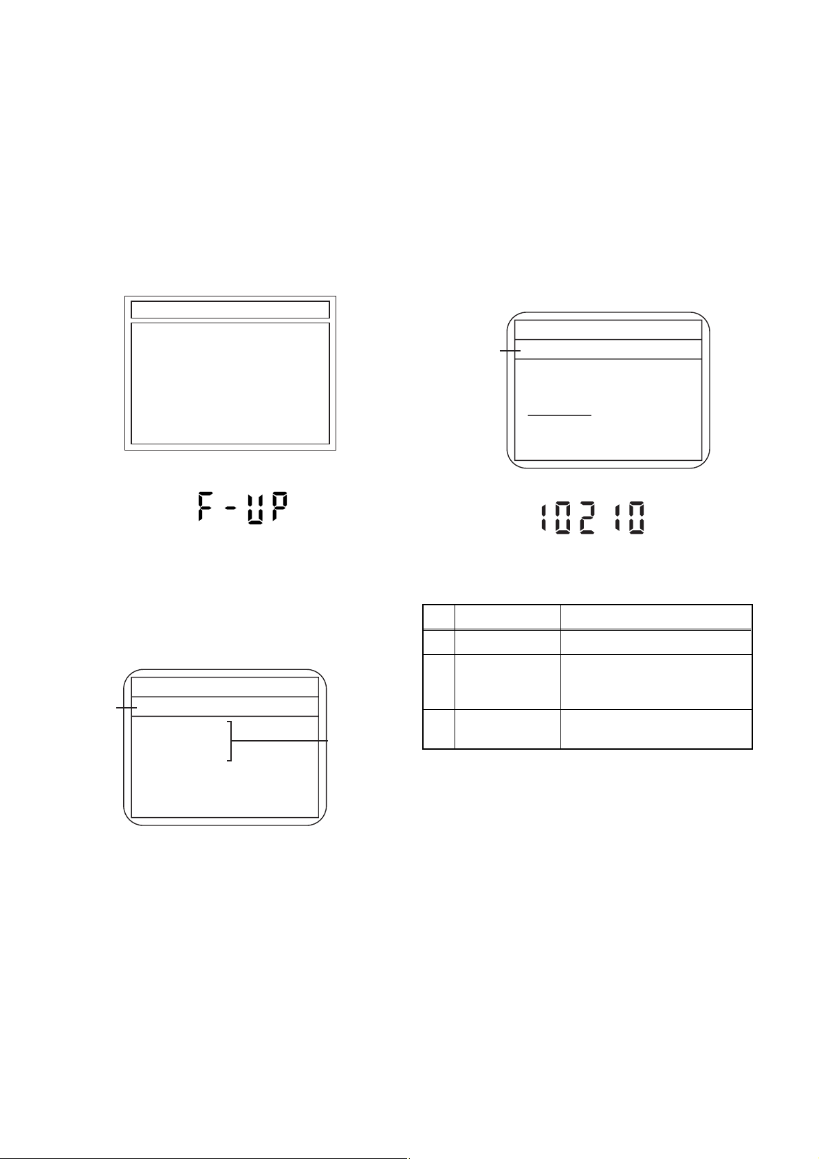
on the VFD. The DVD recorder starts updating.
About VFD indication of Fig. e:
1) When Fig. d is displayed on the screen, “F-UP”
is displayed on the VFD.
2) When “Firmware Updating... XX% Complete.”
is displayed on the screen, “10210” is displayed
on the VFD.
* Firmware Version differs depending on the
models, and this indication is one example.
Firm Update Mode ver.TD5******X2G
Selected
F/W version
is displayed.
TD5T10210X2G
File Loading...
(*1)
Fig. d Programming Mode Screen
Fig. b: VFD Display in Update Mode
4. Load the disc for version up.
Fig. c appears on the screen. The file on the top is
highlighted as the default.
When there is only one file to exist, Step 5 will
start automatically.
* Firmware Version differs depending on the
models, and this indication is one example.
Firm Update Mode ver.TD5******X2G
Disc name
is displayed.
VOL_200703250934
1 TD5T10210X2G
2 TD5T10211X2G
3 TD5T10212X2G
4 TD5T10213X2G
1 / 1
Files included
in the disc are
displayed.
Fig. c: Update Disc TV Screen
Fig. e VFD in Programming Mode (Example)
The appearance shown in (*1) of Fig. d is
described as follows.
No. Appearance State
1 File Loading... Sending files into the memory
Firmware
2
Updating...
Writing new version data
XX% Complete.
Firmware
--Update Failure
Failed in updating
6. After updating is finished, the tray opens
automatically.
At this time, no button is available.
7. Pull out the AC code once, then insert it again.
1-10-1 E3NG1FW
Page 24
How to Verify the Firmware Version
1. Turn the power on and remove the disc in the tray.
2. To switch the HDD & DVD into HDD mode, press
[HDD] on the remote control unit.
3. To put the HDD & DVD into version display mode,
press [VARIABLE SKIP] and [1], [2], [3] buttons on
the remote control unit in that order within 3
seconds. Fig. i appears on the TV screen.
*1: "
*2: Firmware Version differs depending on the
models, and this indication is one example.
Display Contents
" differs depending on the models.
*******
F/W VERSION DISP
MODEL NAME :
DVB-T VERSION :
FE VERSION :
BE VERSION :
TT VERSION :
DV UNIQUE ID :
LD ADJUSTMENT :
DISC ADJUSTMENT :
DEFAULT SETTING : ENTER
EXIT : RETURN
*******
*.**
***_***_***
************
*********
******** ********
OK
OK
Fig. i: Firmware version display
MODEL NAME Model Name
DVB-T
VERSION
DVB-T Module version
FE VERSION Firmware F/E version
BE VERSION Firmware B/E version
TT VERSION Firmware T/T version
DV UNIQUE ID DV Unique ID
LD
ADJUSTMENT
DISC
ADJUSTMENT
LD adjustment progress (done: OK/
not done: --)
Factory adjustment progress (done:
OK/not done: --)
4. Press [RETURN] or [ ] button to turn off.
Note: Be sure to verify the firmware version.
1-10-2 E3NG1FW
Page 25
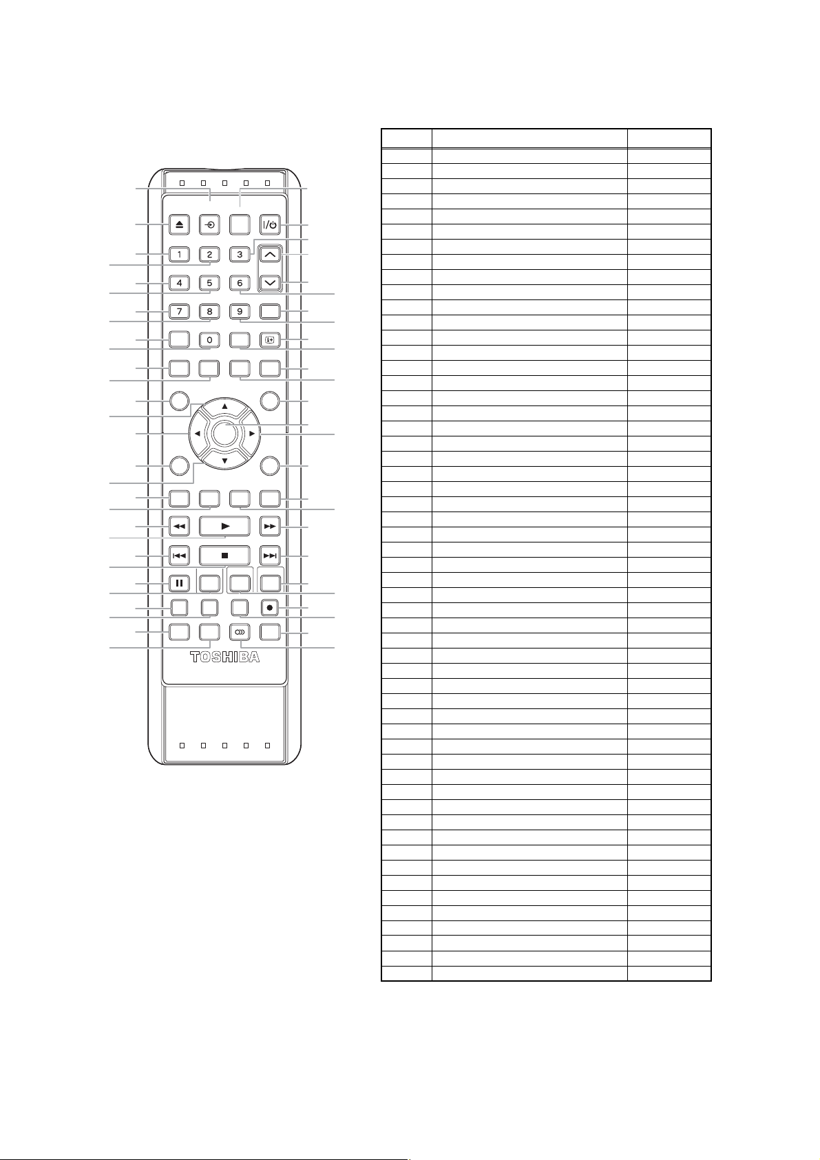
REMOTE CONTROL KEY CODE
NEC Format
10
14
18
22
26
32
35
39
42
45
49
53
Key No.
1 OPEN/CLOSE 45BC-11
2 INPUT SELECT 45BC-0F
2
OPEN/
INPUT
CLOSE HDMI
SELECT
1
.@/:
ABC DEF
5
6
GHI JKL MNO
9
PQRS TUV WXYZ
PROG.
TIMER
PROG.
13
SETUP
17
TEXT
SPACE
VARIABLE
REPLAY
CLEAR INFO
VARIABLE
SKIP
GUIDE
21
TOP MENU
DISC MENU
25
28
DISPLAY
ENTER
/OK
RETURN
/BACK
31
SEARCH
34
REV
PLAY
FWD
38
SKIPSKIP STOP
41
HDD DVD
VCR
PAUSE
44
48
TIME SLIP
SUBTITLE
DUBBING
1.3x/0.8xPLAY
REC MODE
AUDIO
REC
SAT.LINK
52
3
4
7
8
12
16
20
24
27
29
33
37
40
43
47
51
55
11
15
19
23
30
36
46
50
54
SE-R0298
3 HDMI 45BC-B0
4 ON/STANDBY 45BC-12
51 45BC-01
62 45BC-02
73 45BC-03
8 PROG. UP 45BC-1E
94 45BC-04
10 5 45BC-05
11 6 45BC-06
12 PROG. DOWN 45BC-1F
13 7 45BC-07
14 8 45BC-08
15 9 45BC-09
16 TIMER PROG. 45BC-40
17 SETUP 45BC-52
18 0 45BC-00
19 CLEAR 45BC-53
20 INFO 45BC-3F
21 TEXT 45BC-23
22 VARIABLE REPLAY 45BC-55
23 VARIABLE SKIP 45BC-5B
24 GUIDE 45BC-6D
25 TOP MENU 45BC-D0
26 CURSOR UP 45BC-C0
27 DISC MENU 45BC-D1
28 CURSOR LEFT 45BC-CC
29 ENTER/OK 45BC-44
30 CURSOR RIGHT 45BC-C4
31 DISPLAY 45BC-5A
32 CURSOR DOWN 45BC-C8
33 RETURN/BACK 45BC-D2
34 RED 45BC-2A
35 GREEN 45BC-2B
36 YELLOW 45BC-2C
37 BLUE(SEARCH) 45BC-29
38 REV 45BC-98
39 PLAY 45BC-13
40 FWD 45BC-9A
41 SKIP DOWN 45BC-84
42 STOP 45BC-16
43 SKIP UP 45BC-80
44 PAUSE 45BC-17
45 VCR 45BC-1B
46 HDD 45BC-19
47 DVD 45BC-18
48 TIME SLIP 45BC-1A
49 DUBBING 45BC-56
50 REC MODE 45BC-A7
51 REC 45BC-15
52 SUBTITLE 45BC-D5
53 1.3x/0.8x PLAY 45BC-AA
54 AUDIO 45BC-D3
55 SAT.LINK 45BC-1D
Name Code
1-10-3 E3NG1FW
Page 26
NOTE: BOARD MEANS PRINTED CIRCUIT BOARD.
1 Power Supply Section
FLOW CHART NO.1
The power cannot be turned on.
TROUBLESHOOTING
Is the fuse normal?
Ye s
Is normal state restored when once unplugged power
cord is plugged again after several seconds.
Ye s
Is the AL+5V line voltage normal?
Ye s
Check each rectifying circuit of secondary circuit and
replace P1(AV ASSEMBLY) or P3(PW/SW ASSEMBLY)
if defective.
FLOW CHART NO.2
The fuse blows out.
Check the presence that the primary component is
leaking or shorted and replace P3(PW/SW ASSEMBLY)
if defective.
After servicing, replace the fuse.
FLOW CHART NO.3
When the output voltage fluctuates.
No
No
No
See FLOW CHART No.2 <The fuse blows out.>
Check for lead or short-circuiting of primary circuit
component and replace P3(PW/SW ASSEMBLY)
if defective.
(Q1001, Q1003, T1001, D1001, D1002, D1003,
D1004, D1011, R1003)
Check the presence that the rectifying diode or circuit
is shorted in each rectifying circuit of secondary side
and replace P3(PW/SW ASSEMBLY) if defective.
Does the secondary side photo coupler circuit operate
normally?
Ye s
Check the circuit and replace P3(PW/SW ASSEMBLY)
if defective. (IC1001, D1025, D1022, D1023)
FLOW CHART NO.4
When buzz sound can be heard in the vicinity of power circuit.
Check if there is short circuit on the rectifying diode and the circuit in each rectifying circuit of secondary side, and
replace P1(AV ASSEMBLY) if defective. (D013, D014, D016, D018, D019, D1031, D1032, D1033, D1034, D1035,
D1101, D1103, IC1103, IC1104, IC1105, IC1800, Q1100, Q1102, Q1105, Q1106, Q1108, Q1114, Q1502, Q1508,
Q1511, Q1513, Q1516, Q1517, Q1520, Q1521, Q1527, Q1548, Q1550, Q1551)
FLOW CHART NO.5
-FL is not outputted.
Is the supply voltage of -24V fed to the anode of D018?
Ye s
Check Q1550, Q1552, Q1553 and their periphery, and
replace P1(AV ASSEMBLY) if defective.
No
No
Check the circuit and replace P3(PW/SW ASSEMBLY)
if defective. (IC1001, IC1101, D1102)
Check D018 and their periphery, and replace
P3(PW/SW ASSEMBLY) if defective.
1-11-1 E3NG1TR
Page 27
FLOW CHART NO.6
AL+15V is not outputted.
Is the supply voltage 44V fed to the cathode of D013?
Ye s
Check for load circuit short-circuiting or leak, and
replace P1(AV ASSEMBLY) if defective.
FLOW CHART NO.7
TU+30V is not outputted.
Is 44V voltage supplied to emitter of Q1511?
Ye s
Is the "H" pulse (approximately 5V) inputted to
the base of Q1512?
Ye s
Check Q1511, Q1512 and their periphery, and
replace P1(AV ASSEMBLY) if defective.
FLOW CHART NO.8
No
No
No
Check D013 and their periphery, and replace
P3(PW/SW ASSEMBLY) if defective.
Refer to "FLOW CHART NO.6"<AL+15V is not
outputted>.
Check the P-ON-H siganal line, and replace
P1(AV ASSEMBLY) if defective.
AL+12V is not outputted.
Is the supply voltage 12V fed to the cathode of D014?
Ye s
Check for load circuit short-circuiting or leak, and
replace P1(AV ASSEMBLY) if defective.
FLOW CHART NO.9
P-ON+9V is not outputted.
Is 12V voltage supplied to collector of Q1513?
Ye s
Is the "H" pulse (approximately 10V) inputted to
the base of Q1513?
Ye s
Check Q1513 and their periphery, and replace
P1(AV ASSEMBLY) if defective.
No
No
No
Check D014 and their periphery, and replace
P3(PW/SW ASSEMBLY) if defective.
Refer to "FLOW CHART NO.8"<AL+12V is not
outputted>.
Refer to "FLOW CHART NO.7"<TU+30V is not
outputted>.
1-11-2 E3NG1TR
Page 28
FLOW CHART NO.10
P-ON+5V(DECK) is not outputted.
Is 12V voltage supplied to collector of Q1516?
Ye s
Is the "H" pulse (approximately 6V) inputted to
the base of Q1516?
Ye s
Check Q1516 and their periphery, and replace
P1(AV ASSEMBLY) if defective.
FLOW CHART NO.11
AL+5V is not outputted.
Is the supply voltage 5V fed to the cathode of D016?
Ye s
Is the "H" pulse (approximately 5V) inputted to
the base of Q1502?
Ye s
Check Q1502 and their periphery, and replace
P1(AV ASSEMBLY) if defective.
No
No
No
No
Refer to "FLOW CHART NO.8"<AL+12V is not
outputted>.
Refer to "FLOW CHART NO.9"<P-ON+9V is not
outputted>.
Check D016 and their periphery, and replace
P3(PW/SW ASSEMBLY) if defective.
Refer to "FLOW CHART NO.8"<AL+12V is not
outputted>.
FLOW CHART NO.12
P-ON+5V is not outputted.
Is 5V voltage supplied to collector of Q1517?
Ye s
Is the "H" pulse (approximately 5V) inputted to
the base of Q1517?
Ye s
Check Q1517 and their periphery, and replace
P1(AV ASSEMBLY) if defective.
FLOW CHART NO.13
ECO+5V is not outputted.
Is 5V voltage supplied to collector of Q1520?
Ye s
Is the "H" pulse (approximately 6V) inputted to
the base of Q1520?
Ye s
No
No
No
No
Refer to "FLOW CHART NO.11"<AL+5V is not
outputted>.
Refer to "FLOW CHART NO.9"<P-ON+9V is not
outputted>.
Refer to "FLOW CHART NO.11"<AL+5V is not
outputted>.
Refer to "FLOW CHART NO.14"<ECO+9V is not
outputted>.
Check Q1520 and their periphery, and replace
P1(AV ASSEMBLY) if defective.
1-11-3 E3NG1TR
Page 29
FLOW CHART NO.14
ECO+9V is not outputted.
Is 10V voltage supplied to collector of Q1521?
Ye s
Check Q1521 and their periphery, and replace
P1(AV ASSEMBLY) if defective.
FLOW CHART NO.15
ECO+12V is not outputted.
Is 12V voltage supplied to emitter of Q1548?
Ye s
Check Q1548, Q1549 and their periphery, and replace
P1(AV ASSEMBLY) if defective.
FLOW CHART NO.16
P-ON+5V(2) is not outputted.
Is the supply voltage 5V fed to the cathode of D016?
Ye s
No
No
No
Refer to "FLOW CHART NO.15"<ECO+12V is not
outputted>.
Refer to "FLOW CHART NO.8"<AL+12V(2) is not
outputted>.
Check D016 and their periphery, and replace
P3(PW/SW ASSEMBLY) if defective.
Is the "H" pulse (approximately 6V) inputted to
the base of Q1106?
Ye s
Check Q1106 and their periphery, and replace
P3(PW/SW ASSEMBLY) if defective.
FLOW CHART NO.17
P-ON+10V is not outputted.
Is the supply voltage 14V fed to the cathode of D1031?
Ye s
Check IC1102,Q1100,Q1101,Q1105 and their
periphery, and replace P3(PW/SW ASSEMBLY)
if defective.
No
No
Refer to "FLOW CHART NO.17"<P-ON+10V is not
outputted>.
Check D1031 and their periphery, and replace
P3(PW/SW ASSEMBLY) if defective.
1-11-4 E3NG1TR
Page 30
FLOW CHART NO.18
P-ON+3.3V is not outputted.
Is the supply voltage 5V fed to the cathode of D1101?
Ye s
Is the "H" pulse (approximately 5V) inputted to
the base of Q1107?
Ye s
Is 3.3V voltage outputted to pin 2 of IC1104?
Ye s
Check for load circuit short-circuiting or leak, and
replace P1(AV ASSEMBLY) if defective.
FLOW CHART NO.19
SYS+5V is not outputted.
Is 5V voltage outputted to pin 26 of CL1001?
Ye s
Check for load circuit short-circuiting or leak, and
replace P1(AV ASSEMBLY) if defective.
No
No
No
No
Check D1101 and their periphery, and replace
P3(PW/SW ASSEMBLY) if defective.
Check the 1V2CONT signal line, and replace
P1(AV ASSEMBLY) if defective.
Check IC1104 and their periphery, and replace
P3(PW/SW ASSEMBLY) if defective.
Check IC1105 and their periohery, and replace
P3(PW/SW ASSEMBLY) if defective.
FLOW CHART NO.20
P-ON+1.8V is not outputted.
Is 2.5V voltage supplied to pin(1) of IC1800?
Ye s
Check IC1800 and their periohery, and replace
P1(AV ASSEMBLY) if defective.
FLOW CHART NO.21
The fluorescent display tube does not light up.
Is 5V voltage supplied to Pin(13,43) of IC612?
Ye s
Is approximately -24V to -28V voltage supplied to
Pin(30) of IC612?
Ye s
Is there approximately 500kHz oscillation to
Pin(5) of IC612?
Ye s
Are the filament voltage applied between Pin(1)
and Pin(24) of the fluorescent display tube?
Also negative voltage applied between these pins
and GND?
Ye s
Replace P1(AV ASSEMBLY).
No
No
No
No
No
Check D1033 and their periohery, and replace
P3(PW/SW ASSEMBLY) if defective.
Check the ECO+5V line and replace
P1(AV ASSEMBLY) if defective.
Check the -FL line and replace P1(AV ASSEMBLY)
or P3(PW/SW ASSEMBLY) if defective.
Check R618, IC612 and their periphery, and replace
P1(AV ASSEMBLY) if defective.
Check the power circuit, D1103, D1108, R1106, C1110
and their periphery, and replace P3(PW/SW ASSEMBLY)
if defective.
1-11-5 E3NG1TR
Page 31

2 HDD/DVD Section
FLOW CHART NO.1
The key operation is not functioning.
Are the contact point and the installation state of
the key switches normal?
Ye s
Is the control voltage normally inputted into Pin(8) of
IC501?
Ye s
Replace P1(AV ASSEMBLY) or P2(DVD MECHANISM
& DVD/HDD MAIN BOARD ASSEMBLY).
No
No
Re-install the key switches correctly or replace
P3(PW/SW ASSEMBLY).
Check the key switches and their periphery, and replace
P3(PW/SW ASSEMBLY) if defective.
Terminal voltage of IC501-8
4.30
3.60
2.90
2.39
1.98
1.61
1.27
0.92
0.51
(V)
FLOW CHART NO.2
No HDD/DVD operation is possible from the remote control. (Operation is possible from the unit.)
KEY-1
IC501-8
HDD>DVD
VCR>DVD
OPEN
/CLOSE
VCR
HDD
DVD
HDD/DVD
-STOP
HDD/DVD
-PLAY
HDD/DVD
-REC
Is 5V voltage supplied to Pin(3) terminal of the RS1501
(remote control receiver)?
Ye s
Is the "L" pulse sent out from Pin(1) terminal of the
RS1501 (remote control receiver) when the remote
control is activated?
Ye s
Is the "L" pulse signal supplied to Pin(14) of IC501?
Ye s
Replace P1(AV ASSEMBLY) or P2(DVD MECHANISM
& DVD/HDD MAIN BOARD ASSEMBLY).
FLOW CHART NO.3
The [No Disc] indication.
Both picture and sound do not operate normally.
Replace the P2(DVD MECHANISM & DVD/HDD MAIN
BOARD ASSEMBLY).
No
No
No
Check AL+5V line, and replace P1(AV ASSEMBLY) if
defective.
Replace P1(AV ASSEMBLY) or remote control(X1).
Check the line between the RS1501 (remote
control receiver) and Pin(14) of IC501, and replace
P1(AV ASSEMBLY) if defective.
1-11-6 E3NG1TR
Page 32

FLOW CHART NO.4
VIDEO E-E does not appear normally.
Are the video signals inputted to each pin of IC1509? Check the line between video input terminal and
IC1509 VIDEO-IN 1 (AV1)18PIN
IC1509 VIDEO-IN (FRONT)14PIN
IC1509 DTV-Y3PIN
IC1509 DTV-C5PIN
IC1509 VIDEO-IN 2 (AV2)12PIN
IC1509 TUNER-VIDEO
Are the video signals outputted to each pin of IC1509?
IC1509 VIDEO-Y/CVBS-IN61PIN
IC1509 VIDEO-C-IN59PIN
Are the video signals outputted to each pin of CN1502?
CN1502 VIDEO-Y/CVBS-IN20PIN
CN1502 VIDEO-C-IN22PIN
Continued to A on the next page.
20PIN
Ye s
Ye s
Ye s
No
No
No
each pin of IC1509, and replace P1(AV ASSEMBLY),
P6(BOARD DTV MODULE UNIT) or TU1800.
IC1509 → JK150418PIN
IC1509 → CN1800 26PIN3PIN
IC1509 → CN1800 28PIN5PIN
IC1509 → JK200112PIN
Is 5V voltage supplied to Pin(27,29,47,63) of IC1509?
Is 9V voltage supplied to Pin(75) of IC1509?
Ye s N o
Replace P1(AV
ASSEMBLY).
Check the line between each pin of IC1509 and
each pin of CN1502 and replace P1(AV ASSEMBLY)
if defective.
IC1509
IC1509
Check the ECO+5V, ECO+9V
line and replace P1(AV
ASSEMBLY) or P3(PW/SW
ASSEMBLY) if defective.
→ CN150261PIN
→ CN1502 59PIN
VIDEO-IN 1 (AV1)
VIDEO-IN (FRONT)IC1509 → JK300114PIN
DTV-Y
DTV-C
VIDEO-IN 2 (AV2)
TUNER-VIDEOIC1509 → TU1800 17PIN20PIN
20PIN
22PIN
VIDEO-Y/CVBS-IN
VIDEO-C-IN
1-11-7 E3NG1TR
Page 33

A
Are the video signals outputted to each pin of CN1502?
CN1502 VIDEO-Y(I/P)-OUT7PIN
CN1502 VIDEO-Y(I)-OUT1PIN
CN1502 VIDEO-Pr/Cr-OUT5PIN
CN1502 VIDEO-Pb/Cb-OUT3PIN
CN1502 VIDEO-C-OUT
Are the video signals shown above inputted into each
pin of IC1509?
IC1509 VIDEO-Y(I/P)-OUT51PIN
IC1509 VIDEO-Y(I)-OUT55PIN
IC1509 VIDEO-Pr/Cr-OUT52PIN
IC1509 VIDEO-Pb/Cb-OUT53PIN
IC1509 VIDEO-C-OUT57PIN
Are the video signals outputted to each pin of IC1509?
IC1509 VIDEO-OUT 1 (AV1)30PIN
IC1509 VIDEO-OUT 2 (AV2)22PIN
IC1509 VIDEO-Y40PIN
IC1509 VIDEO-Pr/Cr39PIN
IC1509 VIDEO-Pb/Cb38PIN
9PIN
Ye s
Ye s
Ye s
No
No
No
Replace the P2(DVD MECHANISM & DVD/HDD
MAIN BOARD ASSEMBLY).
Check the line between each pin of CN1502 and
each pin of IC1509, and replace P1(AV ASSEMBLY)
if defective.
CN1502 → IC15097PIN
CN1502 → IC15095PIN
CN1502 → IC15093PIN
→ IC1509
9PIN
Is 5V voltage supplied to Pin(27,29,47,63) of IC1509?
Is 9V voltage supplied to Pin(75) of IC1509?
Ye s N o
Replace P1(AV
ASSEMBLY).
51PIN
52PIN
53PIN
57PINCN1502
Check the ECO+5V, ECO+9V
l
ine and replace P1(AV
ASSEMBLY) or P3(PW/SW
ASSEMBLY) if defective.
VIDEO-Y(I/P)-OUT
VIDEO-Y(I)-OUTCN1502 → IC15091PIN 55PIN
VIDEO-Pr/Cr-OUT
VIDEO-Pb/Cb-OUT
VIDEO-C-OUT
Are the video signals outputted to the specific
output terminal?
Are the composite video signals outputted to
the VIDEO OUT (AV1) terminal (JK1504)?
Are the composite video signals outputted to
the VIDEO OUT (AV2) terminal (JK2001)?
Are the component video signals outputted to
the VIDEO OUT terminal (JK1505)?
No
No
No
Check the periphery of JK1504 from Pin (30) of IC1509
and replace P1(AV ASSEMBLY) if defective.
Check the periphery of JK2001 from Pin (22) of IC1509
and replace P1(AV ASSEMBLY) if defective.
Check the periphery of JK1505 from Pin (38, 39, 40) of
IC1509 and replace P1(AV ASSEMBLY) if defective.
1-11-8 E3NG1TR
Page 34

FLOW CHART NO.5
Picture does not appear normally.
Set the disc on the disc tray, and playback it.
(DVD MODE)
Or, playback by selecting the picture in HDD top menu.
(HDD MODE)
Are the video signals outputted to each pin of CN1502?
CN1502 VIDEO-Y(I/P)-OUT7PIN
CN1502 VIDEO-Y(I)-OUT1PIN
CN1502 VIDEO-Pr/Cr-OUT5PIN
CN1502 VIDEO-Pb/Cb-OUT3PIN
CN1502 VIDEO-C-OUT
Are the video signals shown above inputted into each
pin of IC1509?
IC1509 VIDEO-Y(I/P)-OUT51PIN
IC1509 VIDEO-Y(I)-OUT55PIN
IC1509 VIDEO-Pr/Cr-OUT52PIN
IC1509 VIDEO-Pb/Cb-OUT53PIN
IC1509 VIDEO-C-OUT57PIN
Are the video signals outputted to each pin of IC1509?
IC1509 VIDEO-OUT 1 (AV1)30PIN
IC1509 VIDEO-OUT 2 (AV2)22PIN
IC1509 VIDEO-Y40PIN
IC1509 VIDEO-Pr/Cr39PIN
IC1509 VIDEO-Pb/Cb38PIN
Are the video signals outputted to the specific
output terminal?
Are the composite video signals outputted to
the VIDEO OUT (AV1) terminal (JK1504)?
Are the composite video signals outputted to
the VIDEO OUT (AV2) terminal (JK2001)?
Are the component video signals outputted to
the VIDEO OUT terminal (JK1505)?
9PIN
Ye s
Ye s
Ye s
No
No
No
No
No
No
Replace the P2(DVD MECHANISM & DVD/HDD MAIN
BOARD ASSEMBLY).
Check the line between each pin of CN1502 and each
pin of IC1509, and replace P1(AV ASSEMBLY) if
defective.
CN1502
CN1502
CN1502
Is 5V voltage supplied to Pin(27,29,47,63) of IC1509?
Is 9V voltage supplied to Pin(75) of IC1509?
Replace P1(AV
ASSEMBLY).
Check the periphery of JK1504 from Pin (30) of IC1509
and replace P1(AV ASSEMBLY) if defective.
Check the periphery of JK2001 from Pin (22) of IC1509
and replace P1(AV ASSEMBLY) if defective.
Check the periphery of JK1505 from Pin (38, 39, 40) of
IC1509 and replace P1(AV ASSEMBLY) if defective.
→
IC15097PIN
→
IC15091PIN 55PIN
→
→
IC15093PIN
→
9PIN
Ye s N o
IC1509
51PIN
IC15095PIN
52PIN
53PIN
57PINCN1502
Check the ECO+5V, ECO+9V
line and replace P1(AV
ASSEMBLY) or P3(PW/SW
ASSEMBLY) if defective.
VIDEO-Y(I/P)-OUT
VIDEO-Y(I)-OUTCN1502
VIDEO-Pr/Cr-OUT
VIDEO-Pb/Cb-OUT
VIDEO-C-OUT
1-11-9 E3NG1TR
Page 35

FLOW CHART NO.6
Audio E-E does not appear normally.
Check the line between audio input terminal and
each pin of IC1509, and replace P1(AV ASSEMBLY),
P6(BOARD DTV MODULE UNIT) or TU1800 if defective.
Are the audio signals inputted to each pin of IC1509?
IC1509 AUDIO-IN1 (AV1)86,87PIN
IC1509 AUDIO-IN (FRONT)91,92PIN
IC1509 AUDIO-IN2 (AV2)89,90PIN
IC1509 TUNER-AUDIO84,85PIN
IC1509 DTV-AUDIO93,94PIN
Ye s
Are the audio signals outputted to Pin(79,80) of IC1509?
Ye s
Are the audio signals outputted to Pin(11,13) of CN1502?
Ye s
Continued to B on the next page.
No
No
No
→
IC1509
IC1509
IC1509
IC1509
IC1509
Is 5V voltage supplied to Pin(27,29,47,63) of IC1509?
Is 9V voltage supplied to Pin(75) of IC1509?
Replace P1(AV
ASSEMBLY).
Check the line between each pin of IC1509 and
each pin of CN1502, and replace P1(AV ASSEMBLY),
if defective.
IC1509
IC1509 80PIN
91,92PIN
Ye s N o
79PIN
JK150486,87PIN
→
JK3002,
JK3003
→
JK200189,90PIN
→
TU1800 6PIN 84,85PIN
→
CN1800 29,30PIN93,94PIN
Check the ECO+5V, ECO+9V
line and replace P1(AV
ASSEMBLY) or P3(PW/SW
ASSEMBLY) if defective.
→
CN1502 13PIN
→
CN1502 11PIN
AUDIO-IN1 (AV1)
AUDIO-IN (FRONT)
AUDIO-IN2 (AV2)
TUNER-AUDIO
DTV-AUDIO
AUDIO(R)-IN
AUDIO(L)-IN
1-11-10 E3NG1TR
Page 36

B
Are the analog audio signals outputted to each pin of
CN1502?
CN1502 17PIN AUDIO (L)-OUT
CN1502 15PIN AUDIO (R)-OUT
Ye s
Are the analog audio signals inputted to each pin of
IC1509?
IC1509 77PIN AUDIO (L)-OUT
IC1509 76PIN AUDIO (R)-OUT
Ye s
Are the analog audio signals outputted to each pin of
IC1509?
IC1509 73,74PIN AUDIO-OUT 1 (AV1)
IC1509 71,72PIN AUDIO-OUT 2 (AV2)
IC1509 67,68PIN AUDIO-OUT (REAR)
Ye s
Are the audio signals outputted to the specific output
terminal?
Are the audio signals outputted to the audio terminal
(JK1504)?
Are the audio signals outputted to the audio terminal
(JK2001)?
Are the audio signals outputted to the audio terminal
(JK1502)?
No
No
No
No
No
No
Replace the P2(DVD MECHANISM & DVD/HDD MAIN
BOARD ASSEMBLY).
Check each line between each pin of CN1502 and each
pin of IC1509, and replace P1(AV ASSEMBLY) if
defective.
CN1502 17PIN
CN1502 15PIN
Is 5V voltage supplied to Pin(27, 29, 47 ,63) of IC1509?
Is 9V voltage supplied to Pin(75) of IC1509?
Replace P1(AV
ASSEMBLY).
Check the periphery between Pin(73,74) of IC1509
and the audio terminal (JK1504), and replace
P1(AV ASSEMBLY) if defective.
Check the periphery between Pin(71,72) of IC1509
and the audio terminal (JK2001), and replace
P1(AV ASSEMBLY) if defective.
Check the periphery between Pin(67,68) of IC1509
and the audio terminal (JK1502), and replace
P1(AV ASSEMBLY) if defective.
→
IC1509 77PIN AUDIO(L)-OUT
→
IC1509 76PIN AUDIO(R)-OUT
Ye s N o
Check the ECO+5V, ECO+9V
line and replace P1(AV
ASSEMBLY) or P3(PW/SW
ASSEMBLY) if defective.
1-11-11 E3NG1TR
Page 37

FLOW CHART NO.7
Audio is not outputted during playback.
Set the disc on the disc tray, and playback it.
(DVD MODE)
Or, playback by selecting the picture in HDD top menu.
(HDD MODE)
Are the analog audio signals outputted to each pin of
CN1502?
CN1502 17PIN AUDIO (L)-OUT
CN1502 15PIN AUDIO (R)-OUT
Ye s
Are the analog audio signals inputted to each pin of
IC1509?
IC1509 77PIN AUDIO (L)-OUT
IC1509 76PIN AUDIO (R)-OUT
Ye s
Are the analog audio signals outputted to each pin of
IC1509?
IC1509 73,74PIN AUDIO-OUT 1 (AV1)
IC1509 71,72PIN AUDIO-OUT 2 (AV2)
IC1509 67,68PIN AUDIO-OUT (REAR)
Ye s
Are the audio signals outputted to the specific output
terminal?
Are the audio signals outputted to the audio terminal
(JK1504)?
Are the audio signals outputted to the audio terminal
(JK2001)?
Are the audio signals outputted to the audio terminal
(JK1502)?
No
No
No
No
No
No
Replace the P2(DVD MECHANISM & DVD/HDD MAIN
BOARD ASSEMBLY).
Check each line between each pin of CN1502 and each
pin of IC1509, and replace P1(AV ASSEMBLY) if
defective.
CN1502 17PIN
CN1502 15PIN
Is 5V voltage supplied to Pin(27, 29, 47 ,63) of IC1509?
Is 9V voltage supplied to Pin(75) of IC1509?
Replace P1(AV
ASSEMBLY).
Check the periphery between Pin(73,74) of IC1509
and the audio terminal (JK1504), and replace
P1(AV ASSEMBLY) if defective.
Check the periphery between Pin(71,72) of IC1509
and the audio terminal (JK2001), and replace
P1(AV ASSEMBLY) if defective.
Check the periphery between Pin(67,68) of IC1509
and the audio terminal (JK1502), and replace
P1(AV ASSEMBLY) if defective.
→
IC1509 77PIN AUDIO(L)-OUT
→
IC1509 76PIN AUDIO(R)-OUT
Ye s N o
Check the ECO+5V, ECO+9V
line and replace P1(AV
ASSEMBLY) or P3(PW/SW
ASSEMBLY) if defective.
1-11-12 E3NG1TR
Page 38

3 VCR Section
FLOW CHART NO.1
The key operation is not functioning.
Are the contact point and the installation state of the
key switches normal?
Ye s
Is the control voltage normally inputted into Pin(7) of
IC501?
Ye s
Replace P1(AV ASSEMBLY).
No
No
Re-install some key switches correctly or replace
P1(AV ASSEMBLY).
Check the key switches and their periphery, and replace
P1(AV ASSEMBLY) if defective.
Terminal voltage of IC501-7
4.30
3.60
2.90
2.39
1.98
1.61
1.27
0.92
0.51
(V)
KEY-1
IC501-7
S-INH
CH-UP
CH
-DOWN
REC
PLAY
FF
REW
STOP
/EJECT
POWER
FLOW CHART NO.2
No VCR operation is possible from the remote control. (Operation is possible from the unit.)
Is 5V voltage supplied to the Pin(3) terminal of the
RS1501 (remote control receiver)?
Ye s
Is the "L" pulse sent out from Pin(1) terminal of the
RS1501 (remote control receiver) when the remote
control is activated?
Ye s
Is the "L" pulse signal supplied to Pin(14) of IC501?
Ye s
Replace P1(AV ASSEMBLY).
No
No
No
Check AL+5V line and replace P1(AV ASSEMBLY)
if defective.
Replace the RS1501 (remote control receiver).
Replace P1(AV ASSEMBLY) or remote control (X1).
Check the line between the RS1501 (remote control
receiver) and Pin(14) of IC501, and replace P1(AV
ASSEMBLY) if defective.
1-11-13 E3NG1TR
Page 39

FLOW CHART NO.3
Cassette tape can not be loaded.
When loading a cassette tape, on Pin(100) of IC501,
does the "L" pulse switch to the "H" pulse?
Ye s
When loading a cassette tape, is the specified voltage
(approximately 13V) outputted to the terminal of the
Loading Motor Unit?
Ye s
Replace DECK ASSEMBLY (1B1).
FLOW CHART NO.4
Cassette tape is ejected right after the loading.
When loading a cassette tape, on Pin(100) of IC501,
does the "L" pulse switch to the "H" pulse?
Ye s
When loading a cassette tape, on Pin(4) of IC501,
does the "L" pulse switch to the "H" pulse?
Ye s
When loading a cassette tape, does the LD-SW
operate normally?
Ye s
Replace P1(AV ASSEMBLY).
No
No
No
No
No
Check the line between the start sensor and Pin(100)
of IC501, and replace P1(AV ASSEMBLY) if defective.
Replace DECK ASSEMBLY (1B1).
Check the line between the start sensor and Pin(100)
of IC501, and replace P1(AV ASSEMBLY) if defective.
Check the line between the end sensor and Pin(4)
of IC501, and replace P1(AV ASSEMBLY) if defective.
Check the line between the LD-SW(SW507) and Pin(9)
of IC501, and replace P1(AV ASSEMBLY) if defective.
FLOW CHART NO.5
Cassette tape can not be ejected.
When pressing the eject button, does the Capstan
Motor start rotating?
Ye s
While the Capstan Motor is rotating, is the Takeup
Reel rotating?
Ye s
While the Takeup Reel is rotating, is the reel pulse
signal inputted to Pin(80) of IC501?
Ye s
While the reel pulse signal is inputting, is "L" pulse
outputted to Pin(81) of IC501?
Ye s
Is the specified vo ltage (approximately 13V)
outputted to the terminal of the Lading Motor Unit?
Ye s
Is the Loading Motor rotating?
Ye s
Check the Cam Gear or Rack Assembly, etc.,
and replace DECK ASSEMBLY (1B1) if defective.
No
No
No
No
No
No
Refer to "FLOW CHART NO.6 " <The Capstan Motor
does not rotate>.
Check the Reel Disc or Clutch Assembly, and replace
DECK ASSEMBLY (1B1). it if defective.
Check the line between the Takeup Reel sensor and
Pin(80) of IC501, and replace P1(AV ASSEMBLY) if
defective.
Replace P1(AV ASSEMBLY).
Replace DECK ASSEMBLY (1B1).
Replace DECK ASSEMBLY (1B1).
1-11-14 E3NG1TR
Page 40

FLOW CHART NO.6
Capstan Motor does not rotate.
Is 5V voltage supplied to Pin(2) of CN502?
Ye s
Is over approximately 2.6V voltage supplied to Pin(5)
of CN502?
Ye s
Is 12V voltage supplied to Pin(1) of CN502?
Ye s
Replace DECK ASSEMBLY (1B1).
FLOW CHART NO.7
Drum Motor does not rotate.
Is 5V voltage supplied to Pin(2) of CN502?
Ye s
Is over approximately 2.6V voltage supplied to
Pin(8) of CN502?
Ye s
Is 12V voltage supplied at Pin(11) of CN502?
Ye s
Replace DECK ASSEMBLY (1B1).
No
No
No
No
No
No
Check the P-ON+5V line and replace P1(AV ASSEMBLY)
if defective.
Check the line between Pin(5) of CN502 and Pin(76) of
IC501, and replace P1(AV ASSEMBLY) if defective.
Check AL+16V/+12V line, and replace P1(AV ASSEMBLY)
if defective.
Check the P-ON+5V line and replace P1(AV ASSEMBLY)
if defective.
Check the line between Pin(8) of CN502 and Pin(77) of
IC501, and replace P1(AV ASSEMBLY) if defective.
Check the AL+12V line, and replace P1(AV ASSEMBLY)
if defective.
FLOW CHART NO.8
Drum Motor rotates only for a few seconds.
Is the D-PFG signal inputted to Pin(90) of IC501?
Ye s
Is the RF-SW signal outputted to Pin(18) of IC501?
Ye s
Is 12V voltage supplied Pin(11) of CN 502?
Ye s
Replace DECK ASSEMBLY (1B1).
FLOW CHART NO.9
RF-SW signal is not outputted.
Is the Drum Motor rotating?
Ye s
Is the D-PFG signal inputted to Pin(90) of IC501?
Ye s
Replace P1(AV ASSEMBLY).
No
No
No
No
No
Replace DECK ASSEMBLY (1B1).
Replace P1(AV ASSEMBLY).
Check the AL+12V line, and replace P1(AV ASSEMBLY)
if defective.
D-PG
D-FG
5Vp-p
Refer to "FLOW CHART NO.7" <Drum Motor does
not rotate> and "FLOW CHART NO.8" <Drum Motor
rotates only for a few seconds>.
Replace DECK ASSEMBLY (1B1).
D-FG
2.5Vp-p
1-11-15 E3NG1TR
Page 41

FLOW CHART NO.10
Video E-E does not appear normally.
Are the video signals inputted to each pin of IC1509? Check the line between video input terminal and each
IC1509 VIDEO-IN 1 (AV1)18PIN
IC1509 VIDEO-IN (FRONT)14PIN
IC1509 VIDEO-IN 2 (AV2)12PIN
IC1509 TUNER-VIDEO
IC1509 DTV-Y3PIN
IC1509 DTV-C5PIN
Are the video signals outputted to Pin(24) of IC1509?
Is the video signal inputted to Pin(48) of IC301?
20PIN
Ye s
Ye s
Ye s
No
No
No
pin of IC1509, and replace P1(AV ASSEMBLY), P6
(BOARD DTV MODULE UNIT) or TU1800 if defective.
→
IC1509
IC1509
IC1509
Is 5V voltage supplied to Pin(27,29,47,63) of IC1509?
Is 9V voltage supplied to Pin(75) of IC1509?
Ye s N o
Replace P1(AV
ASSEMBLY).
Check the line between Pin(24) of IC1509 and Pin(48)
of IC301, and replace P1(AV ASSEMBLY) if defective.
JK150418PIN
→
JK300114PIN
→
JK200112PIN
→
TU180020PIN 17PIN
→
CN18003PIN
→
CN18005PIN
Check the ECO+5V, ECO+9V
line and replace P1(AV
ASSEMBLY) if defective.
VIDEO-IN 1 (AV1)
VIDEO-IN (FRONT)IC1509
VIDEO-IN 2 (AV2)
TUNER-VIDEOIC1509
26PIN
28PIN
DTV-Y
DTV-CIC1509
Is the C-SYNC signal outputted to Pin(67) of IC301?
Ye s N o
Is the C-SYNC signal inputted to Pin(58) of IC501? Is 5V voltage supplied to Pin(18,24,42,55,72,91) of
Ye s
Check the line between Pin(67)
of IC301 and Pin(58) of IC501,
and replace P1(AV ASSEMBLY)
if defective.
Is the video signal inputted into Pin(100) of IC1509?
Ye s
Are the video signals outputted to each pin of IC1509?
IC1509 30PIN VIDEO-OUT 1 (AV1)
IC1509 22PIN VIDEO-OUT 2 (AV2)
Ye s
Are the video signals outputted to the specific output
terminal?
Are the composite video signals outputted to the
VIDEO-OUT terminal (JK1504)?
No
Replace P1(AV
ASSEMBLY).
No
No
No
IC301?
Ye s
Check the P-ON+5V line and AL+5V line,
and replace P1(AV ASSEMBLY) if
defective.
Ye s
Is the serial data and clock signal supplied to Pin(68,69)
of IC301?
No
Check the line between Pin(68,69) of IC301 and Pin
(71, 72) of IC501, and replace P1(AV ASSEMBLY) if
defective.
Check the line between Pin(61) of IC301 and Pin(100)
of IC1509, and replace P1(AV ASSEMBLY) if defective.
Is 5V voltage supplied to Pin(27,29,47,63) of IC1509?
Is 9V voltage supplied to Pin(75) of IC1509?
Ye s N o
Replace P1(AV
ASSEMBLY).
Check the periphery of JK1504 from Pin(30) of IC1509
and replace P1(AV ASSEMBLY) if defective.
Check the ECO+5V, ECO+9V
line and replace P1(AV
ASSEMBLY) if defective.
No
Are the composite video signals outputted to the
VIDEO-OUT terminal (JK2001)?
No
Check the periphery of JK2001 from Pin(22) of IC1509
and replace P1(AV ASSEMBLY) if defective.
1-11-16 E3NG1TR
Page 42

FLOW CHART NO.11
Hi-Fi E-E audio does not operate normally.
Are the audio signals inputted to each pin of IC1509?
IC1509 AUDIO-IN1 (AV1)86,87PIN
IC1509 AUDIO-IN (FRONT)91,92PIN
IC1509 AUDIO-IN2 (AV2)89,90PIN
IC1509 TUNER-AUDIO84,85PIN
IC1509 DTV-AUDIO93,94PIN
Ye s
No
Check the line between audio input terminal and each
pin of IC1509, and replace P1(AV ASSEMBLY), P6
(BOARD DTV MODUDLE UNIT) or TU1800 if defective.
IC1509
IC1509 JK3002,
IC1509
IC1509
IC1509
91,92PIN
→
JK150486,87PIN
→
JK3003
→
JK200189,90PIN
→
TU1800 6PIN84,85PIN
→
CN1800 29,30PIN 93,99PIN
AUDIO-IN1 (AV1)
AUDIO-IN (FRONT)
AUDIO-IN2 (AV2)
TUNER-AUDIO
DTV-AUDIO
Are the audio signals outputted to Pin(69,70) of IC1509?
Ye s
Is the audio signal inputted to Pin(4,50) of IC451?
Ye s
Is the 5V voltage supplied to Pin(16,32,35,36,46,55) of
I
C451, and the 9V voltage supplied to Pin(69) of IC451?
Ye s
Is the serial data and the clock signal supplied to
Pin(37,38) of IC451?
Ye s
Is the audio signal outputted to Pin(74,76) of IC451?
Ye s
Is the audio signal inputted into Pin(81,82) of IC1509?
Ye s
No
No
No
No
No
No
Is 5V voltage supplied to Pin(27,29,47,63) of IC1509?
Is 9V voltage supplied to Pin(75) of IC1509?
Ye s N o
Replace P1(AV
ASSEMBLY).
Check the line between Pin(69,70) of IC1509 and
Pin(4,50) of IC451, and replace P1(AV ASSEMBLY)
if defective.
Check the circuit of AL+5V, P-ON+5V and P-ON+9V,
and replace P1(AV ASSEMBLY) if defective.
Check the line between Pin(37,38) of IC451 and
Pin(71,72) of IC501, and replace P1(AV ASSEMBLY)
if defective.
Replace P1(AV ASSEMBLY).
Check the line between Pin(74,76) of IC451 and
Pin(81,82) of IC1509, and replace P1(AV ASSEMBLY)
if defective.
Check the ECO+5V, ECO+9V
line and replace P1(AV
ASSEMBLY) if defective.
Are the audio signals outputted to each pin of IC1509?
IC1509 73,74PIN AUDIO-OUT 1 (AV1)
IC1509 71,72PIN AUDIO-OUT 2 (AV2)
Ye s
Are the audio signals outputted to the specific output
terminal?
Are the audio signals outputted to the audio terminal
(JK1504)?
Are the audio signals outputted to the audio terminal
(JK2001)?
No
No
No
Is 5V voltage supplied to Pin(27,29,47,63) of IC1509?
Is 9V voltage supplied to Pin(75) of IC1509?
Ye s N o
Replace P1(AV
ASSEMBLY).
Check the line between Pin(73,74) of IC1509 and audio
terminal (JK1504), and replace P1(AV ASSEMBLY) if
defective.
Check the line between Pin(71,72) of IC1509 and audio
terminal (JK2001), and replace P1(AV ASSEMBLY) if
defective.
Check the ECO+5V, ECO+9V
line and replace P1(AV
ASSEMBLY) if defective.
1-11-17 E3NG1TR
Page 43

FLOW CHART NO.12
Hi-Fi audio can not be recorded normally. (E-E mode is normal.)
Is the Hi-Fi-COM signal outputted to Pin(26) of IC451?
Ye s
Is the line between Pin(8) of CN251 and Pin(26) of
IC451 normal?
Ye s
Replace DECK ASSEMBLY (1B1).
FLOW CHART NO.13
Hi-Fi audio can not be playbacked normally. (Hi-Fi E-E mode is normal.)
Is the Playback Envelope signal outputted to Pin(33) of
IC451?
Ye s
Replace P1(AV ASSEMBLY).
FLOW CHART NO.14
Audio can not be recorded normally in the linear audio mode. (E-E mode is normal.)
No
No
No
Replace P1(AV ASSEMBLY).
Check the line between Pin(8) of CN251 and Pin(26)
of IC451, and replace P1(AV ASSEMBLY) if defective.
Is the Hi-Fi-H-SW signal inputted into to Pin(39) of IC451?
Ye s
Replace P1(AV
ASSEMBLY).
No
Check the Hi-Fi-H-SW line between
Pin(39) of IC451 and Pin(19) of
IC501, and replace P1(AV
ASSEMBLY) if defective.
Is the audio signal inputted into Pin(13) of IC301?
Ye s
Does the Bias oscillation circuit operate normally?
Ye s
Is the audio signal outputted to Pin(11) of IC301?
Ye s
Is the audio signal outputted to Pin(100) of IC301?
Ye s
Replace DECK ASSEMBLY (1B1).
No
No
No
No
Check the line between Pin(78) of IC451 and Pin(13)
of IC301, and replace P1(AV ASSEMBLY) if defective.
Check the Bias oscillation circuit (
Q405,Q406)
Replace P1(AV ASSEMBLY).
Replace P1(AV ASSEMBLY).
and replace P1(AV ASSEMBLY) if defective.
Q401,Q403,Q404,
1-11-18 E3NG1TR
Page 44

FLOW CHART NO.15
Audio can not be playbacked normally in the linear audio mode. (E-E mode is normal.)
Is the audio signal supplied to Pin(5) of IC301?
No
Is there no dirt on the surface of ACE head assembly?
Ye s
Is the height of ACE head assembly appropriate?
Ye s
Replace DECK ASSEMBLY (1B1).
Ye s
No
No
Is the audio signal outputted to Pin(11) of IC301?
NoYe s
Check the line between Pin(11)
of IC301 and Pin(80) of IC451,
and replace P1(AV ASSEMBLY).
Clean the surface of ACE head assembly.
Readjust the height of the ACE head assembly.
Replace P1(AV
ASSEMBLY).
1-11-19 E3NG1TR
Page 45

FUNCTION INDICATOR SYMBOLS
< VCR Section >
When the power comes on again after that by pressing [ ] button, an error message is displayed on the TV
screen as follows.
When reel or capstan mechanism is not functioning
correctly
A
R
SP 0:00:00
Fig. 1
When tape loading mechanism is not functioning
correctly
A
T
SP 0:00:00
Fig. 2
When cassette loading mechanism is not functioning
correctly
P-ON+5V Power safety detection
A
P
SP 0:00:00
Fig. 5
A
C
SP 0:00:00
When the drum is not working properly
A
D
SP 0:00:00
Fig. 3
Fig. 4
1-12-1 E3NG1FIS
Page 46

< HDD/DVD Section >
Note: If an error occurs, a message with the error number appears on the screen.
Recording Error
Message Solution
Can not record on this disc.
This program is not allowed to
be recorded.
This program is not recordable
in Video mode.
This program is not allowed to
be recorded on this disc.
You cannot record on this disc as
Power Calibration Area is full.
E35
Insert a recordable disc, and
ensure the disc status satisfies
the recording requirements.
You cannot record copyprohibited programs.
You cannot record copyprohibited programs.
You cannot record cop-y
prohibited programs.
Error message
Error No.
Error
No.
1 An error occurs during data reading.
There is no reply for 15 seconds in Test
2
Unit Ready.
Cannot write the data after trying three
3
times.
4 An error occurs with OPC.
5 During recovery in a record.
An error occurs even if recovery has been
6
tried three times.
7 An error occurs in a format.
8 It cannot start an encode.
NV_PCK/RDI_PCK is not in encoded
9
data.
Encode Pause condition continued for 10
10
minutes.
Encode Pause condition continued in
11
normal REC condition for 10 minutes.
Difference in the address and cannot get
12
Stream ID of RDI/VIDEO.
13 It is a reply that “ATAPI is not readable.”
Cannot write the data after recovering
14
SMALL VMGI.
Cannot write the data after DVD-R
15
Reverse Track.
16 An error occurs in Finalize Close.
17 An error occurs in Rec Stop Close.
18 An error occurs in PCA Full (DVD_R).
19 Safety Stop occurs during editing.
20 High Speed Disc.
21 The disc is not formatted.
22 Disc Error has occurred.
23 The -R Disc of VR Mode.
24 The disc except DVD-R/-RW/+R/+RW.
25 During the Macrovision picture input.
26 During the CGMS picture input.
During the CGMS picture input. (Video
27
Format Disc)
During the CGMS picture input. (VR
28
Format Disc that is not compatible with
CPRM.)
Error Description
1-12-2 E3NG1FIS
Page 47

Message Solution
This disc is protected and not
recordable.
Disc is full.
(No area for new recording)
You cannot record more than
99 titles on one disc. (The
maximum is 99.)
You cannot record more than
999 chapters on one disc.
(The maximum is 999.)
You cannot record on this as
Control Information is full.
Release the disc protection
setting in the Disc Setting
menu.
Insert a recordable disc with
enough recording space.
Delete unnecessary titles.
Delete unnecessary chapters. 33
Insert a new disc. 34
Error
No.
Error Description
29 Disc Protected Disc.
30 No available recording space.
The 99 title limit has been reached.
31
(Video Format Disc)
The 99 title limit has been reached. (VR
32
Format Disc)
999 chapter limit has been reached. (VR
Format Disc)
No available recording space for Control
Information.
You cannot record on this disc
as Power Calibration Area is
Insert a new disc. 35 PCA is Full. (in REC start)
full.
This disc is already finalized.
Release the finalizing for this
disc.
36 It is finalized. (Video Format Disc)
37 Access to outside of Memory Area.
Can not record on this disc. Repeat the same operation.
38 Sector Address is wrong.
39 BUP writing error of chapter editing.
You cannot record more than
49 titles on the disc. (The
maximum is 49.)
You cannot record more than
254 chapters on the disc. (The
maximum is 254.)
This program is not recordable
in +VR mode.
The disc has no recording
compatibility. Set “Make
Recording Compatible” to
“ON” to convert the disc.
You cannot record more than
600 titles on HDD. (The
maximum is 600.)
Delete unnecessary titles. 43
Delete unnecessary chapter
marks.
You cannot record copyprohibited programs.
Set “Make Recording
Compatible” to “ON” to convert
the disc.
Delete unnecessary titles. 47
The 49 title limit has been reached. (+VR
Format Disc)
The 254 chapter limit has been reached.
44
(+VR Format Disc)
During the CGMS picture input (+VR
45
Format Disc).
Trying to record onto the +VR formatting
disc that had been recorded by the other
46
recorder when “Make Recording
Compatible” setting is “OFF”,
The 600 title limit has been reached
(HDD).
Can not record on this HDD. Connect HDD. 48 Recording without HDD connected.
The REC key was pushed when HDD
was full.
HDD is full.
Delete unnecessary titles. 49
Delete unnecessary titles. 50 HDD is full during recording.
This Program is not allowed to
be recorded.
Receive PAL/SECAM signal. 51
When you receive signal other than PAL/
SECAM.
If an error occurs during the timer recording, one of the following error numbers (40 to 42) or the above
error messages (error number: 1 to 39 and 43 to 51) is displayed on the recording menu after timer
recording.
(Once the screen of the program line is exited, the program line for the error will be cleared.)
(No Error Message is displayed for errors No. 40 ~ 42.)
Timer Programming
THU
Error number
Date Start End
'
New Programme
566.
CH
2&%
A program with the error number is grayed out on the timer programming list.
1-12-3 E3NG1FIS
Page 48

Message Solution
Error message is not
displayed.
Error
No.
- Set the timer programming
correctly.
- Set the timer programming
before the start time.
Turn the power on and set the
clock correctly then set timer
programming again.
Insert the recordable disc. 42 No disc when recording
- Some portion has not been recorded
because of program overlapping.
40
- Recording did not start at the start time.
41 Power failed
Error Description
1-12-4 E3NG1FIS
Page 49

Servo/System Control Block Diagram
BLOCK DIAGRAMS
NOTE: BOARD MEANS PRINTED CIRCUIT BOARD.
(DECK ASSEMBLY)
ACE HEAD ASSEMBLY
CONTROL
HEAD
Q504
ST-S
BOARD SENSOR
Q503
END-S
BOARD SENSOR
CYLINDER ASSEMBLY
DRUM
M
MOTOR
LOADING
MOTOR
M
PG
SENSOR
CN504
5 CTL(+)
6 CTL(-)
CAPSTAN MOTOR
CAPSTAN
MOTOR
M
TO SUB
POWER SUPPLY
BLOCK DIAGRAM
TP502
END-S
MOTOR
DRIVE
CIRCUIT
SW507
LD-SW
D555
S-LED
P-DOWN-H
C-POW-SW
P-ON-H
ECO-MODE
AL+5V
AL+5V
CN502
3 C-FG
C-F/R
4
C-CONT
5
LM-FWD/REV
7
D-CONT
8
D-PFG
9
Q506
T-REEL
VR501
SW-POINT
SYS+5V
SYS+5V
AL+5V
RS1501
REMOTE
SENSOR
PS502
S-REEL
D520
VCR-REC
AL+5V
SW506
REC-SAFETY
Q514
RESET
TP503
CTL
IC501
(SERVO/SYSTEM CONTROL)
LD-SW
9
CTL(+)
95
CTL(-)
94
ST-S
100
END-S
4
T-REEL
80
S-REEL
79
CTL
97
PG-DELAY
2
Q520
23
VCR-REC-LED
87
C-FG
78
C-F/R
C-CONT
76
81
LM-FWD/REV
D-CONT77
90
D-PFG
31
REC-SAF-SW
RESET
34
REMOTE
14
32 P-DOWN-H
82 C-POW-SW
75 P-ON-H
73 ECO-MODE
DRV-DATA
DRV-CLK
DRV-STB
VCR-AUDIO-MUTE
Hi-Fi-H-SW
A-MODE
IIC-BUS SDA
IIC-BUS SCL
D-REC-H
RF-SW
C-ROTA
D-V-SYNC
H-A-SW
H-A-COMP
V-ENV
C-SYNC
BOARD AV
(VFD DRIVER)
IC612
42
1G
36
HDD-LED
DVD-LED
VCR-LED
POWER-LED
7G
20
P1
23
P2
25
P4
28
P5
26
P7
21
P8
22
P9
4
2
3
1
VCR-AUDIO-MUTE
68
70
69
27
19
28
72
71
33
18
15
13
16
17
6
58
7
DRV-DIN
8
DRV-CLK
9
DRV-STB
GRID
SEGMENT
HDD-LED
DVD-LED
VCR-LED
POWER-LED
IIC-BUS SDA
IIC-BUS SCL
IIC-BUS SDA
IIC-BUS SCL
IIC-BUS SDA
IIC-BUS SCL
IIC-BUS SDA
IIC-BUS SCL
IIC-BUS SDA
IIC-BUS SCL
Hi-Fi-H-SW
A-MODE
IIC-BUS SDA
IIC-BUS SCL
D-REC-H
RF-SW
C-ROTA
D-V-SYNC
H-A-SW
H-A-COMP
V-ENV
C-SYNC
FL601
VFD
TO SUB SYSTEM
CONTROL
BLOCK DIAGRAM
TO DTV MODULE
BLOCK DIAGRAM
TO AUDIO SELECTOR
BLOCK DIAGRAM
TO VIDEO SELECTOR
BLOCK DIAGRAM
TO AUDIO
BLOCK DIAGRAM
TO Hi-Fi AUDIO
BLOCK DIAGRAM
TO VIDEO
BLOCK DIAGRAM
1-13-1
E3NG1BLS
Page 50

Sub System Control Block Diagram
1V2CONT
TO SUB
POWER SUPPLY
BLOCK DIAGRAM
TO DTV MODULE
BLOCK DIAGRAM
IC101
(MAIN MICRO CONTROLLER)
POW-SW
LOW-POW
FAN-CONT1
REG-CONT
DTV-SYS-RESET
DTV-TXD
DTV-RXD
DTV-S-SCLK
IC501
(SUB MICRO CONTROLLER)
DVD/HDD-AUDIO-MUTE
25
1V2CONT
POW-SW
59
LOW-POW
74
FAN-CONT1
11
REG-CONT
60
AUDIO-MUTE
SC-AUDIO-MUTE
DVD-REC-LED
HDD-REC-LED
NOTE: BOARD MEANS PRINTED CIRCUIT BOARD.
26
29
30
21
22
DVD/HDD-AUDIO-MUTE
CN1504
4
DVD-REC-LED
3
HDD-REC-LED
5
6
1
AUDIO-MUTE
SC-AUDIO-MUTE
CN3011
4
3
5
VCR-LED
6
DVD-LED
1
HDD-LED
TO AUDIO SELECTOR
BLOCK DIAGRAM
BOARD FRONT JACK
ECO+5V
D3001
Q3001
DRIVE
Q3002
DRIVE
D3002
D3005
D3003
D3004
DVD-REC
HDD-REC
VCR
DVD
HDD
DTV-S-SCLK
DTV-RXD
DTV-TXD
DTV-SYS-RESET
SYS-RESET
SUB-RXD
SUB-TXD
SUB-SCLK
RDY
CLK 27 IN
R23
W25
R22
A4
AL+2.8V
R25
V25
W26
P22
B4
L1
IC107
RESET
2 1
IC501
4 2
X501
27MHz
X'TAL
CN502-D
CN701
5
DTV-S-SCLK
4 DTV-RXD
3 DTV-TXD
2
DTV-SYS-RESET
27 SYS-RESET
30 SUB-RXD
28 SUB-TXD
26 SUB-SCLK
29 RDY
CN1801
5
4
3
2
X501
12MHz
RESONATOR
X502
CN1502
27
30
28
26
29
32KHz
X'TAL
Q517
Q516
39
X OUT
X IN
38
XC OUT
36
XC IN
35
63
SYS-RESET
66
SUB-RXD
65
SUB-TXD
67
SUB-SCLK
64
RDY
DVD/HDD MAIN BOARD BOARD AV
1-13-2
KEY-1
KEY-2
7
8
20DUBBING-LED
KEY SWITCH
CN1505
POWER-LED
3
POWER-SW
2
J917
S-INH
CN1504 CN3011 CN3012
KEY-2
9
DUBBING-LED
2
CN1601
1
3
2
2
SW1601
POWER
BOARD POWER SWITCH
9
KEY SWITCH
2
Q3006
DRIVE
BOARD FRONT JACK BOARD SWITCH
HDD-LED
DVD-LED
VCR-LED
POWER-LED
D1605
POWER
P-ON+5V
TO SERVO/SYSYTEM
CONTROL
BLOCK DIAGRAM
KEY-2
1
DUBBING-LED
4
CN3003
1
4
KEY SWITCH
ECO+5V
D3012
DUBBING
E3NG1BLSS
Page 51

Digital Signal Process Block Diagram
IC101
FRONT-END
DIGITAL
SIGNAL
PROCESS
HARD
DISK
DRIVE
DVD MECHANISM
PICK
-UP
CN3001 CN3002
BOARD ATA
TILT
TRACKING
FOCUS
TRAY OPEN
CN1001-R
CN652
CN201
CN301
P-ON+3.3V
IC201
RF/
ERROR
AMP
IC301
MOTOR
DRIVER
IC202
OP AMP
IC302
LPC
(MAIN MICRO CONTROLLER/MPEG2 AV CODEC)
BACK-END
DIGITAL
SIGNAL
PROCESS
VIDEO
I/F
U4,W1,W3,
Y2,AA1,AA2
P3,T3,T5,
U2,U3,V1
AUDIO
I/F
VIDEO
ENCODER
D/A
D/A
D/A
D/A
D/A
D/A
D/A
HDMI-SDA
HDMI-SCL
VIDEO-CLOCK
IC701 (VIDEO DECODER)
DECODER A/D45-50
DECODER
39-44
N2
P1
M1
N3
M2
D1
D3
R4
K2
K1
N4
Y26
U24
E12
M3
NOTE: BOARD MEANS PRINTED CIRCUIT BOARD.
PB VIDEO SIGNALREC VIDEO SIGNAL PB AUDIO SIGNALREC AUDIO SIGNAL
F2
F1
K5
M5
J3
A5,B5-B7
,C6,C7,
D6,D7
N23
U25
C5
HDMI-SDA
HDMI-SCL
VIDEO-CLOCK
8
10
13
A/D
PCM-DATA0
PCM-BCK
PCM-LRCK
PCM-SCLK
IC802 (AUDIO A/D CONVERTER)
7
8
9
10
AUDIO A/D
CONVERTER
11
12
6
YC(0-7)
SPDIF
L-CH
R-CH
TO VIDEO
BLOCK
DIAGRAM
TO VIDEO
BLOCK
DIAGRAM
13
14
CN701
VIDEO-Y(I/P)-OUT
VIDEO-Pr/Cr-OUT
VIDEO-Pb/Cb-OUT
VIDEO-Y(I)-OUT
VIDEO-C-OUT
VIDEO-Y/CVBS-IN
VIDEO-C-IN
AUDIO(L)-OUT
AUDIO(R)-OUT
DVD/HDD-AUDIO-MUTE
CN701
7
5
3
1
9
20
22
17
15
18
11AUDIO(L)-IN
13AUDIO(R)-IN
TO VIDEO
SELECTOR
BLOCK
DIAGRAM
(CN1502)
TO AUDIO
SELECTOR
BLOCK
DIAGRAM
(CN1502)
SLED
MOTOR
M
SPINDLE
MOTOR
M
CN1002-R
BOARD
RELAY
MOTOR
DRIVER
IC104, IC105
(FLASH MEMORY)
FLASH MEMORY
IC102 (DDR2 SDRAM)
DDR SDRAM
DVD/HDD MAIN BOARD
1-13-3
LINK
I/F
AA3
AC2
AB3
AC3
AA4
AE1
AA5
AD1
W5
AC1
JK1502
(REAR)
CN901
DIGITAL
AUDIO OUT
(COAXIAL)
1TPA1P
2TPA1N
TO
DV JACK
4TPB1P
(W11)
5TPB1N
33SPDIF
LINK
I/F
CN1001
BOARD
POWER
SUPPLY
RECEIVE
DATA
DECODER
TRANSMIT
DATA
ENCODER
CL1001
28 28SPDIF
30
29
28
27
CN1503
WF10
Q1535
BUFFER
BOARD AV
CN101
IC901 (IEEE1394 I/F)
4
Y5
Y4
5
6
7
8
9
10
11
1
48
2
3
E3NG1BLD
Page 52

Video Selector Block Diagram
BOARD
REAR JACK
Q2001
JK2001
VIDEO OUT2
VIDEO-G
VIDEO-B
VIDEO-R
TO DIGITAL
SIGNAL
PROCESS
BLOCK
DIAGRAM
(CN701)
19
11
7
15
20
22 VIDEO-C-IN
7
5
3
1
9
CN2001 CN1506
BUFFER
CN1502
VIDEO-Y/CVBS-IN
VIDEO-Y(I/P)-OUT
VIDEO-Pr/Cr-OUT
VIDEO-Pb/Cb-OUT
VIDEO-Y(I)-OUT
VIDEO-C-OUT
VIDEO-OUT288
VIDEO-G-IN13 13
VIDEO-B-IN12 12
VIDEO-R-IN14 14
Q1515
BUFFER
Q1514
WF8
WF4
WF7WF5
BUFFER
(VIDEO SELECTOR)IC1509
DRIVER FBC
22
48
50
49
61
59
51
52
53
55
57
MUTE
MUTE
NOTE: BOARD MEANS PRINTED CIRCUIT BOARD.
REC VIDEO SIGNAL PB VIDEO SUGNAL
BOARD AV
SW
GCL
LPF
64
SW
65
SW
SW
+
AGC
SW
SW
SW
62
CN1506 CN2001
12
18
14
20
CN1504 CN3011
VIDEO-IN210 10
JK1504
20
VIDEO IN1
VIDEO-IN15 15
JK2001
20
BOARD
REAR JACK
JK3001
(FRONT)
BOARD FRONT JACK
VIDEO
IN2
VIDEO
-IN
VIDEO OUT1
VIDEO-G
VIDEO-B
VIDEO-R
JK1504
19
11
7
15
VIDEO-Y
-OUT
VIDEO-Pb/Cb
-OUT
VIDEO-Pr/Cr
-OUT
JK1505
(REAR)
TO VIDEO
BLOCK
DIAGRAM
Q1541
BUFFER
VCR-VIDEO-OUT
VCR-VIDEO-IN
WF6
DRIVER
30
46
DRIVER
44
DRIVER
45
DRIVER
40
DRIVER
38
DRIVER
39
DRIVER
24
MUTE FBC
SW
SW
SW
SW
SW
SW
+
1-13-4
SW
SW
LPF
SW
SW
AGC
SW
100
3
5
IIC
I/F
42
43
17
16
IIC-BUS SDA
IIC-BUS SCL
DTV-Y
DTV-C
TU1800
(TUNER UNIT)
VIDEO-OUT
IC700 (VPS)
VPS-V
TO SERVO/SYSTEM
CONTROL
BLOCK DIAGRAM
TO DTV MODULE
BLOCK DIAGRAM
E3NG1BLVS
Page 53

Video Block Diagram
Q402
TO VIDEO
SELECTOR
BLOCK DIAGRAM
VCR-VIDEO-OUT
VCR-VIDEO-IN
BUFFER
IC501 (OSD)
OSD
CHARACTER
52
MIX
NOTE: BOARD MEANS PRINTED CIRCUIT BOARD.
REC VIDEO SIGNAL
50
IC301
VIDEO SIGNAL
PROCESS
WF1
/HEAD AMP
48
PB/EE
56
MUTE
61
65
BYPASS AGC
CHARA.
INS.
FBC
PR
AGC
6968 46 43
SERIAL
DECODER
1/2
Y/C
MIX
PB VIDEO SIGNAL
Y. DELAY
LUMINANCE
SIGNAL
PROCESS
CCD 1H DELAY
CHROMINANCE
SIGNAL
PROCESS
VXO
IIC-BUS SCL
IIC-BUS SDA
7978
R
P
Y
+
C
RPRP
REC AUDIO SIGNAL PB AUDIO SIGNAL
TO SERVO/SYSTEM
SP
EP
REC
FM
AGC
RF-SW/C-ROTA
D-V-SYNC
H-A-COMP
CONTROL
BLOCK DIAGRAM
96
SP
95
HEAD
94
AMP
93
90
EP
89
HEAD
88
AMP
87
D-REC-H
80
70
62
71
H-A-SW
83
84
V-ENV
C-SYNC
67
CN251
VIDEO(R)-1
VIDEO-COM
VIDEO(L)-1
VIDEO(L)-2
VIDEO-COM
VIDEO(R)-2
(DECK ASSEMBLY)
CYLINDER ASSEMBLY
1
2
3
4
5
6
WF2
TP504
RF-SW
D-REC-H
RF-SW
C-ROTA
D-V-SYNC
H-A-SW
H-A-COMP
V-ENV
C-SYNC
VIDEO (R)-1
HEAD
VIDEO (L)-1
HEAD
VIDEO (L)-2
HEAD
VIDEO (R)-2
HEAD
TO SERVO/SYSTEM
CONTROL
BLOCK DIAGRAM
DVD/HDD MAIN BOARD
ICA01 (HDMI INTERFACE)
TO DIGITAL SIGNAL PROCESS BLOCK DIAGRAM
HDMI-SCL
HDMI-SDA
PCM-DATA0
SPDIF
PCM-SCLK
PCM-LRCK
PCM-BCK
YC(0-7)
VIDEO-CLOCK
113
IIC
I/F
114
38
43
33
41
45
81
~
83
86
~
90
111
117
I/F
AUDIO
VIDEO
I/F
REGISTER
CONTROLLER
TP301
C-PB
WF3
21
58 59
QA01,QA02
DRIVE
ICA02
3.3V<-->5V
CONVERTER
AUTHENT
/CATION
KEY
EXCHANGE
AV
HDCP
CIPHER/
ENCRYPTOR
TMDS
ENCODER
119
DDC
121
I/F
120
22
24
TMDS
TRANSMITTER
18
20
14
16
12
10
2
3
6
5 16
P-ON+5V
X301
4.43MHz
CNA01
HDMI-CONNECTOR
HOT PLUG
19
DETECT
15
SCL
SDA
T.M.D.S DATA2-
3
1
T.M.D.S DATA2+
6
T.M.D.S DATA1-
4
T.M.D.S DATA1+
9
T.M.D.S DATA0-
7
T.M.D.S DATA0+
10
T.M.D.S CLOCK+
12
T.M.D.S CLOCK-
2928
BOARD AV
1-13-5
E3NG1BLV
Page 54

Audio Selector Block Diagram
BOARD AV
IIC-BUS SDA
IIC-BUS SCL
IC1508
(OP AMP)
OP
2
6
IC1506
OP AMP
(
1
7
VCR-AUDIO-OUT(L)
VCR-AUDIO-OUT(R)
AMP
OP
AMP
OP
AMP
OP
AMP
1
7
)
2
6
TO DIGITAL
SIGNAL
PROCESS
BLOCK
DIAGRAM
(CN701)
TO SERVO/SYSTEM
CONTROL
BLOCK DIAGRAM
CN1502
17
AUDIO(L)-OUT
15
AUDIO(R)-OUT
18
DVD/HDD-AUDIO-MUTE
11 AUDIO(L)-IN
13 AUDIO(R)-IN
WF9
TO Hi-Fi
AUDIO
BLOCK
DIAGRAM
IC1509(AUDIO SELECTOR)
42
IIC
I/F
43
77
76
SW
SW
80
70
79
69
SW
SW
SW
SW
REC AUDIO SIGNAL PB AUDIO SIGNAL
72
SW
71
SW
74
SW
73
SW
68
SW
67
SW
90
87
85
92
(VCR DVD/HDD DUBBING)
(DVD/HDD VCR DUBBING)
82
94
89
86
84
91
81
93
NOTE: BOARD MEANS PRINTED CIRCUIT BOARD.
CN1506 CN2001
66
AUDIO(L)-IN2
55
AUDIO(R)-IN2
33
AUDIO(L)-OUT2
11
AUDIO(R)-OUT2
22
AUDIO-MUTE
Q1537
MUTE-ON
Q1534
DRIVE
31
30
MUTE-ON
MUTE-ON
Q1536
DRIVE
CN1504 CN3011
BOARD REAR JACK
MUTE-ON
Q2003
JK1504
Q1538
MUTE-ON
IC1902
(IF SIGNAL PROCESS)
L-CH
IF SIGNAL
R-CH
PROCESS
Q1539
Q1540
17 17
AUDIO(L)-IN
19 19
AUDIO(R)-IN
VCR-AUDIO-IN(L)
VCR-AUDIO-IN(R)
AUDIO-MUTE
SC-AUDIO-MUTE
DVD/HDD-AUDIO-MUTE
DTV-AUDIO(L)
DTV-AUDIO(R)
JK2001
MUTE-ON
Q2002
AUDIO(L)-IN16
AUDIO(R)-IN1
2
AUDIO(L)-OUT1
3
AUDIO(R)-OUT1
1
2
BOARD FRONT JACK
TO Hi-Fi AUDIO
BLOCK DIAGRAM
TO SUB SYSTEM
CONTROL
BLOCK DIAGRAM
TO DTV MODULE
BLOCK DIAGRAM
AUDIO(L)-IN26
2
AUDIO(R)-IN2
AUDIO(L)-OUT2
3
AUDIO(R)-OUT2
1
TU1800
(TUNER UNIT)
SIF-OUT
6
(REAR)
JK1502
AUDIO(L)
-OUT
AUDIO(R)
-OUT
(FRONT)
JK3002
AUDIO(L)
-IN
JK3003
(FRONT)
AUDIO(R)
-IN
1-13-6
E3NG1BLAS
Page 55

Audio Block Diagram
NOTE: BOARD MEANS PRINTED CIRCUIT BOARD.
TO Hi-Fi AUDIO
BLOCK DIGRAM
(DECK ASSEMBLY)
ACE HEAD ASSEMBLY
AUDIO
HEAD
AUDIO
ERASE
HEAD
N-A-PB
N-A-REC
CN504
4
AUDIO-PB/REC
3 A-COM
1 AE-H
2 FE-H
Q403
BIAS
OSC
Q404
P-ON+5V
Q406
BOARD AV
IC301
(AUDIO SIGNAL PROCESS)
PB-ON
5
6
1
2
SP/LP-ON
AUTO
BIAS
EQ
AMP
REC AUDIO SIGNAL
13
ALC
INV
98
7
3
100
ATT
REC
AMP
DET
ALC
LINE
AMP
REC-ON
MUTE
R
P
PB AUDIO SIGNAL
12
11
FULL
ERASE
HEAD
FE HEAD
CN501
2 FE-H
1 FE-H-GND
Q405
Q401
SWITCHING
PB-ON
SWITCHING
D-REC-OFF
P-ON+5V
1-13-7
AUDIO HD-SW
CONTROL
16
SERIAL
DECODER
68 69
71
VCR-AUDIO-MUTE
IIC-BUS SDA
IIC-BUS SCL
TO SERVO/SYSTEM
CONTROL
BLOCK DIAGRAM
E3NG1BLA
Page 56

Hi-Fi Audio Block Diagram
NOTE: BOARD MEANS PRINTED CIRCUIT BOARD.
TO AUDIO
SELECTOR
BLOCK DIAGRAM
TO AUDIO
BLOCK DIAGRAM
VCR-AUDIO-OUT(R)
VCR-AUDIO-OUT(L)
N-A-REC
N-A-PB
IC451 (Hi-Fi AUDIO SIGNAL PROCESS)
47
R-CH
50
INSEL
4
NOR
SW
78
80
L-CH
INSEL
48
14
15
R-CH
PNR
L-CH
PNR
BOARD AV
P
R
LIM DEV
LIM DEV
R
P
SW
NOISE
SW
NOISE
COMP
VCO
OUTPUT
SELECT
HOLD
PULSE
NOISE
DET
VCO
COMP
R-CH
BPF
LPF
MIX
LPF
L-CH
BPF
COMP
DO
DET
LIM
SERIAL
DATA
DECODER
34 33
MUTE-ON
MUTE-ON
ENV
DET
R
L
REC AUDIO SIGNAL
VCR-AUDIO-IN(L)
VCR-AUDIO-IN(R)
Hi-Fi-
Hi-Fi
Hi-Fi-
CN251
AUDIO(R)
-COM 8
AUDIO(L)
IIC-BUS SDA
IIC-BUS SCL
A-MODE
Hi-Fi-H-SW
(DECK ASSEMBLY)
7
9
37
38
77
76
74
73
39
75
26
21
24
27
Q451
PB AUDIO SIGNAL
TO AUDIO
SELECTOR
BLOCK DIAGRAM
TO
SERVO/ SYSTEM
CONTROL
BLOCK DIAGRAM
Hi-Fi
AUDIO(R)
HEAD
Hi-Fi
AUDIO(L)
HEAD
1-13-8
CYLINDER ASSEMBLY
E3NG1BLH
Page 57

Power Supply Block Diagram
CAUTION !
For continued protection against fire hazard,
replace only with the same type fuse.
HOT CIRCUIT. BE CAREFUL.
NOTE:
The voltage for parts in hot circuit is measured using
hot GND as a common terminal.
NOTE: BOARD MEANS PRINTED CIRCUIT BOARD.
CAUTION !
Fixed voltage (or Auto voltage selectable) power supply circuit is used in this unit.
If Main Fuse (F1001) is blown , check to see that all components in the power supply
circuit are not defective before you connect the AC plug to the AC power supply.
Otherwise it may cause some components in the power supply circuit to fail.
AC1001
F1001
T2.5A H 250V
L1003
LINE
FILTER
D1001 - D1004
BRIDGE
RECTIFIER
Q1003
Q1001
T1001
3
5
7
8
IC1001
ERROR
VOLTAGE DET
4
CL1001
18
17
16
Q1108,Q1110,Q1111
15
14
13
12
11
10
1
+8.5V REG.
Q1101
Q1100
SW+12V
IC1102
SHUNT
Q1104
REG.
Q1102
Q1106
SW+5V
IC1105
+5V REG.
Q1105
+10V REG.
Q1114
Q1115
1 AL-30V
2 AL+44V
3,4 AL+16.3V
7,8
12
14,15
16,17
26 SYS+5V
25
24
11
34 LOW-POW
29 POW-SW
13
27
30,31
32
CN1002
1 FAN+12V
2 GND
CN1003
1 HDD+12V
3 HDD+5V
AL+12V
P-ON+10V
P-ON+5V
AL+5V(3)
F1
F2
1V2CONT
FAN-CONT1
REG-CONT
AL+2.8V
P-ON+3.3V
TO SUB
POWER SUPPLY
BLOCK DIAGRAM
(CN1503)
FAN
HARD
DISK
DRIVE
3
2
IC1101
3
SHUNT
1
REG.
2
HOT COLD
Q1103
1-13-9
BOARD POWER SUPPLY
SW+5V
Q1112
Q1107Q1109
IC1103
+1.8V REG.
IC1104
+3.3V REG.
CN1001
25-27
20-22
10-12
15-17
P-ON+10.5V
P-ON+5V
AL+2.8V
6,7
P-ON+1.8V
P-ON+3.3V
TO
DVD/HDD
MAIN BOARD
(CN101)
E3NG1BLP
Page 58

Sub Power Supply Block Diagram
NOTE: BOARD MEANS PRINTED CIRCUIT BOARD.
TO
POWER SUPPLY
BLOCK DIAGRAM
(CL1001)
CN1503
1 AL-30V
2 AL+44V
3,4 AL+16.3V
7,8
AL+12V
12
P-ON+10V
14,15
P-ON+5V
16,17
AL+5V(3)
26 SYS+5V
25
F1
24
F2
1V2CONT
11
34 LOW-POW
29 POW-SW
13
FAN-CONT1
27
REG-CONT
30,31
AL+2.8V
32
P-ON+3.3V
Q1508
IC1800
+1.8V REG.
Q1554
Q1509
Q1800
Q1548
Q1502
Q1511
+9V REG.
Q1521
Q1512
Q1513
Q1520
Q1516
Q1550
Q1553
Q1552
Q1517
Q1527
-FL
AL+15V
TU+30V
AL+16V/+12V
P-ON+9V(2)
P-ON+5V(DECK)
AL+12V(2)
P-ON+10V
P-ON+3.3V
P-ON+5V(2)
AL+5V
P-ON+5V
SYS+5V
P-ON+1.8V
ECO+12V
ECO+9V
ECO+5V
Q1549
1-13-10
BOARD AV
Q1528
Q1551
P-DOWN-H
P-ON-H
C-POW-SW
ECO-MODE
1V2CONT
LOW-POW
POW-SW
FAN-CONT1
REG-CONT
F1
F2
TO SERVO/SYSTEM
CONTROL
BLOCK DIAGRAM
TO SUB SYSTEM
CONTROL
BLOCK DIAGRAM
E3NG1BLSP
Page 59

DTV Module Block Diagram
IC2500
TU1800
(TUNER UNIT)
DIF-OUT1
DIF-OUT2
DIF-AGC
CN1800 CN2700
11
18
19
20
DIF-OUT1
22
DIF-OUT2
33
DIF-AGC
(DVB-T DEMODULATOR)
30
ADC
/AGC I/F
31
/DEMOD.
39
/DECODER
RESET
SDA
SCL
IC2602 (DTV SIGNAL PROCESS)
93
50
95
49
96
48
47
64
1
44
43
97
94
100
102
103
RESET
SDA
SCL
DTV
DIGITAL SIGNAL
PROCESS
VIDEO
ENCODER
AUDIO
INTERFACE
SDRAM
I/F
DTV-SYS-RESET
VIDEO
D/A
CONVERTER
AUDIO
D/A
CONVERTER
AUDIO-MUTE
SPI-DATA0
SPI-DATA1
SPI-CLK
SPI-CE
DTV-RXD
118
122
L-CH
110
R-CH
109
101
IC2603
(MEMORY)
15
2
SPI-DATA0
SPI-DATA1
13
5
SPI-CLK
16
6
SPI-CE
17
1
105
106
44
DATA BUS(0-15)
*1
ADDRESS BUS(0-11)
*2
IC2901
(OP AMP)
2
6
Q2903
DRIVE
1
7
NOTE: BOARD MEANS PRINTED CIRCUIT BOARD.
REC VIDEO SIGNAL REC AUDIO SIGNAL
CN1800
CN1800CN2700
DTV-Y
DTV-C
DTV-AUDIO(L)
DTV-AUDIO(R)
DTV-TXD
DTV-RXD
DTV-SYS-RESET
DTV-S-SCLK
P-ON+5V
MUTE
-ON
Q2901
CN2701
11 26DTV-Y
13 28DTV-C
14 29
15 30
MUTE
-ON
Q2900
15 15DTV-TXDDTV-TXD
14 14DTV-RXD
12 12
DTV-AUDIO(L)
DTV-AUDIO(R)
DTV-SYS-RESET
TO VIDEO
SELECTOR
BLOCK DIAGRAM
TO AUDIO
SELECTOR
BLOCK DIAGRAM
TO SUB SYSTEM
CONTROL
BLOCK DIAGRAM
SCL
SDA
*1 51,53~59,65~72
*2 64,75~80,86~89,91
*3 22~26,29~35
*4 2,4,5,7,8,10,11,13,42,44,45,
47,48,50,51,53
15
SDA
14
SCL
9
10
IC2800 (DDR SDRAM)
DDR SDRAM
BOARD DTV MODULE UNIT
*3
*4
Q1801
CN1800CN2700
44TU-SDA
55TU-SCL
LEVEL
SHIFTER
Q1802
LEVEL
SHIFTER
Q1805
Q1804,Q1807
SW
Q1803,Q1806
SW
IIC-BUS SDA
IIC-BUS SCL
TO SERVO/
SYSTEM
CONTROL
BLOCK
DIAGRAM
BOARD AV
1-13-11
E3NG1BLDTV
Page 60

SCHEMATIC DIAGRAMS / BOARD’S AND TEST POINTS
NOTE: BOARD MEANS PRINTED CIRCUIT BOARD.
Standard Notes
WARNING
Many electrical and mechanical parts in this chassis
have special characteristics. These characteristics
often pass unnoticed and the protection afforded by
them cannot necessarily be obtained by using
replacement components rated for higher voltage,
wattage, etc. Replacement parts that have these
special safety characteristics are identified in this
manual and its supplements; electrical components
having such features are identified by the mark " ! "
in the schematic diagram and the parts list. Before
replacing any of these components, read the parts list
in this manual carefully. The use of substitute
replacement parts that do not have the same safety
characteristics as specified in the parts list may create
shock, fire, or other hazards.
Notes:
1. Do not use the part number shown on these
drawings for ordering. The correct part number is
shown in the parts list, and may be slightly different
or amended since these drawings were prepared.
2. All resistance values are indicated in ohms
3
(K=10
3. Resistor wattages are 1/4W or 1/6W unless
otherwise specified.
4. All capacitance values are indicated in μF
(P=10
5. All voltages are DC voltages unless otherwise
specified.
6. Electrical parts such as capacitors, connectors,
diodes, IC’s, transistors, resistors, switches, and
fuses are identified by four digits. The first two
digits are not shown for each component. In each
block of the diagram, there is a note such as shown
below to indicate these abbreviated two digits.
, M=106).
-6
μF).
1-14-1 T5P_SC
Page 61

LIST OF CAUTION, NOTES, AND SYMBOLS USED IN THE SCHEMATIC DIAGRAMS ON
THE FOLLOWING PAGES:
1. CAUTION:
FOR CONTINUED PROTECTION AGAINST FIRE HAZARD, REPLACE ONLY WITH THE SAME TYPE FUSE.
2. CAUTION:
Fixed Voltage (or Auto voltage selectable) power supply circuit is used in this unit.
If Main Fuse (F1001) is blown, first check to see that all components in the power supply circuit are not
defective before you connect the AC plug to the AC power supply. Otherwise it may cause some components
in the power supply circuit to fail.
3. Note:
1. Do not use the part number shown on the drawings for ordering. The correct part number is shown in the
parts list, and may be slightly different or amended since the drawings were prepared.
2. To maintain original function and reliability of repaired units, use only original replacement parts which are
listed with their part numbers in the parts list section of the service manual.
4. Voltage indications for PLAY and REC modes on the schematics are as shown below:
< DVD/DVR Section >
231
5.0
The same voltage for
both PLAY & STOP modes
5.0
(2.5)
Indicates that the voltage
is not consistent here.
5. How to read converged lines
1-D3
Distinction Area
Line Number
(1 to 3 digits)
Examples:
1. "1-D3" means that line number "1" goes to the line number
"1" of the area "D3".
2. "1-B1" means that line number "1" goes to the line number
"1" of the area "B1".
6. Test Point Information
: Indicates a test point with a jumper wire across a hole in the BOARD.
: Used to indicate a test point with a component lead on foil side.
: Used to indicate a test point with no test pin.
PLAY mode
STOP mode
< VCR Section >
5.0
The same voltage for
both PLAY, REC & DVD
modes
5.0
(2.5)
< >
PLAY mode
REC mode
DVD mode
231
Indicates that the voltage
is not consistent here.
3
AREA D3
2
1
AREA B1
1-D3
ABCD
Unit: Volts
1-B1
: Used to indicate a test point with a test pin.
1-14-2 T5P_SC
Page 62

AV 1/9 Schematic Diagram < VCR Section >
NOTE: BOARD MEANS PRINTED CIRCUIT BOARD.
1-14-3
E3NG1SCAV1
Page 63

AV 2/9 , POWER SWITCH & SENSOR Schematic Diagram < VCR Section >
7G
6G
5G 4G 3G 2G 1G
PM
S1
DTV BS CS
DR
T
CD
C
a
VCR
f
b
g
DB
HDD
e
c
d
DVD
NOTE: BOARD MEANS PRINTED CIRCUIT BOARD.
FL601 MATRIX CHART
7G 6G 5G 4G 3G 2G 1G
P1
a
a
a
a
a
a
P2
P3
P4
P5
P6
P7 d
P8 S1
P9
PM
b
f
g
c
e
b
f
g
c
e
d
DTV
b
b
f
f
g
g
c
c
e
e
d
d
T
BS CS DR
CD
b
b
f
f
VCR
g
g
DB
c
c
HDD
e
e
d
d
DVD
C
1-14-4
E3NG1SCAV2
Page 64

AV 3/9 Schematic Diagram < VCR Section >
NOTE: BOARD MEANS PRINTED CIRCUIT BOARD.
1-14-5
E3NG1SCAV3
Page 65

AV 4/9 Schematic Diagram < VCR Section >
NOTE: BOARD MEANS PRINTED CIRCUIT BOARD.
1-14-6
E3NG1SCAV4
Page 66

AV 5/9 Schematic Diagram < VCR Section >
NOTE: BOARD MEANS PRINTED CIRCUIT BOARD.
1-14-7
E3NG1SCAV5
Page 67

AV 6/9 Schematic Diagram < VCR Section >
NOTE: BOARD MEANS PRINTED CIRCUIT BOARD.
1-14-8
E3NG1SCAV6
Page 68

AV 7/9 Schematic Diagram < VCR Section >
NOTE: BOARD MEANS PRINTED CIRCUIT BOARD.
1-14-9
E3NG1SCAV7
Page 69

AV 8/9 Schematic Diagram < VCR Section >
NOTE: BOARD MEANS PRINTED CIRCUIT BOARD.
1-14-10
E3NG1SCAV8
Page 70

AV 9/9 Schematic Diagram < VCR Section >
NOTE: BOARD MEANS PRINTED CIRCUIT BOARD.
1-14-11
E3NG1SCAV9
Page 71

POWER SUPPLY Schematic Diagram < VCR Section >
CAUTION !
Fixed voltage (or Auto voltage selectable) power supply circuit is used in this unit.
If Main Fuse (F1001) is blown , check to see that all components in the power supply
circuit are not defective before you connect the AC plug to the AC power supply.
Otherwise it may cause some components in the power supply circuit to fail.
CAUTION !
For continued protection against fire hazard,
replace only with the same type fuse.
NOTE: BOARD MEANS PRINTED CIRCUIT BOARD.
NOTE:
The voltage for parts in hot circuit is measured using
hot GND as a common terminal.
1-14-12
E3NG1SCP
Page 72

FRONT JACK & SWITCH Schematic Diagram < VCR Section >
NOTE: BOARD MEANS PRINTED CIRCUIT BOARD.
1-14-13
E3NG1SCFJ
Page 73

REAR JACK Schematic Diagram < VCR Section > ATA Schematic Diagram < DVD/HDD Section >
NOTE: BOARD MEANS PRINTED CIRCUIT BOARD.
1-14-14
E3NG1SCRJ
E3NG1SCAT
Page 74

DVD/HDD MAIN 1/7 Schematic Diagram < DVD/HDD Section >
1 NOTE:
The order of pins shown in this diagram is different from that of actual IC101.
IC101 is divided into six and shown as IC101 (1/6) ~ IC101 (6/6) in this DVD/HDD Main Schematic Diagram Section.
NOTE: BOARD MEANS PRINTED CIRCUIT BOARD.
1-14-15
E3NG1SCD1
Page 75

DVD/HDD MAIN 2/7 Schematic Diagram < DVD/HDD Section >
1 NOTE:
The order of pins shown in this diagram is different from that of actual IC101.
IC101 is divided into six and shown as IC101 (1/6) ~ IC101 (6/6) in this DVD/HDD Main Schematic Diagram Section.
NOTE: BOARD MEANS PRINTED CIRCUIT BOARD.
1-14-16
E3NG1SCD2
Page 76

DVD/HDD MAIN 3/7 Schematic Diagram < DVD/HDD Section >
1 NOTE:
The order of pins shown in this diagram is different from that of actual IC101.
IC101 is divided into six and shown as IC101 (1/6) ~ IC101 (6/6) in this DVD/HDD Main Schematic Diagram Section.
NOTE: BOARD MEANS PRINTED CIRCUIT BOARD.
1-14-17
E3NG1SCD3
Page 77

DVD/HDD MAIN 4/7 Schematic Diagram < DVD/HDD Section >
1 NOTE:
The order of pins shown in this diagram is different from that of actual IC101.
IC101 is divided into six and shown as IC101 (1/6) ~ IC101 (6/6) in this DVD/HDD Main Schematic Diagram Section.
NOTE: BOARD MEANS PRINTED CIRCUIT BOARD.
1-14-18
E3NG1SCD4
Page 78

DVD/HDD MAIN 5/7 Schematic Diagram < DVD/HDD Section >
1 NOTE:
The order of pins shown in this diagram is different from that of actual IC101.
IC101 is divided into six and shown as IC101 (1/6) ~ IC101 (6/6) in this DVD/HDD Main Schematic Diagram Section.
NOTE: BOARD MEANS PRINTED CIRCUIT BOARD.
1-14-19
E3NG1SCD5
Page 79

DVD/HDD MAIN 6/7 Schematic Diagram < DVD/HDD Section >
NOTE: BOARD MEANS PRINTED CIRCUIT BOARD.
1-14-20
E3NG1SCD6
Page 80

DVD/HDD MAIN 7/7 Schematic Diagram < DVD/HDD Section >
1 NOTE:
The order of pins shown in this diagram is different from that of actual IC101.
IC101 is divided into six and shown as IC101 (1/6) ~ IC101 (6/6) in this DVD/HDD Main Schematic Diagram Section.
NOTE: BOARD MEANS PRINTED CIRCUIT BOARD.
1-14-21
E3NG1SCD7
Page 81

DTV MODULE Schematic Diagram
NOTE: BOARD MEANS PRINTED CIRCUIT BOARD.
1-14-22
E3NG1SCDTV
Page 82

BOARD AV Top View
VR501
SW-POINT
TP503
CTL
WF2
TP504
RF-SW
WF3
TP301
C-PB
TO BOARD SENSOR
(END-SENSOR)
NOTE: BOARD MEANS PRINTED CIRCUIT BOARD.
BOARD SENSOR View
BHF300F01012A
BHF300F01012B
J917
S-INH
TO BOARD SENSOR (START-SENSOR)
1-14-23
J184
AV1-V-OUT1
BE3N00F01011A
Page 83

BOARD AV Bottom View
WF6
PIN 30 OF
IC1509
WF10
PIN 28 OF
CN1503
WF7
PIN 3 OF
CN1502
WF8
PIN 5 OF
CN1502
WF4
PIN 7 OF
CN1502
WF5
PIN 9 OF
CN1502
WF9
PIN 17 OF
CN1502
NOTE: BOARD MEANS PRINTED CIRCUIT BOARD.
WF1
PIN 56 OF
IC301
1-14-24
BE3N00F01011A
Page 84

BOARD POWER SUPPLY Top View
NOTE: BOARD MEANS PRINTED CIRCUIT BOARD.
CAUTION !
For continued protection against fire hazard,
replace only with the same type fuse.
NOTE:
The voltage for parts in hot circuit is measured using
hot GND as a common terminal.
CAUTION !
Fixed voltage (or Auto voltage selectable) power supply circuit is used in this unit.
If Main Fuse (F1001) is blown , check to see that all components in the power supply
circuit are not defective before you connect the AC plug to the AC power supply.
Otherwise it may cause some components in the power supply circuit to fail.
Because a hot chassis ground is present in the power
supply circut, an isolation transformer must be used.
Also, in order to have the ability to increase the input
slowly, when troubleshooting this type power supply
circuit, a variable isolation transformer is required.
1-14-25
BE3N00F01021A
Page 85

BOARD POWER SUPPLY Bottom View
NOTE: BOARD MEANS PRINTED CIRCUIT BOARD.
CAUTION !
For continued protection against fire hazard,
replace only with the same type fuse.
NOTE:
The voltage for parts in hot circuit is measured using
hot GND as a common terminal.
CAUTION !
Fixed voltage (or Auto voltage selectable) power supply circuit is used in this unit.
If Main Fuse (F1001) is blown , check to see that all components in the power supply
circuit are not defective before you connect the AC plug to the AC power supply.
Otherwise it may cause some components in the power supply circuit to fail.
Because a hot chassis ground is present in the power
supply circut, an isolation transformer must be used.
Also, in order to have the ability to increase the input
slowly, when troubleshooting this type power supply
circuit, a variable isolation transformer is required.
1-14-26
BE3N00F01021A
Page 86

BOARD FRONT JACK Top View
NOTE: BOARD MEANS PRINTED CIRCUIT BOARD.
BOARD FRONT JACK Bottom View
BE3N00F01021B
BOARD SWITCH
Top View
BOARD SWITCH
Bottom View
BE3N00F01021C
1-14-27
Page 87

BOARD REAR JACK Top View BOARD REAR JACK Bottom View
NOTE: BOARD MEANS PRINTED CIRCUIT BOARD.
BE3N00F01021D
BOARD POWER SWITCH
Top View
BOARD POWER SWITCH
Bottom View
BE3N00F01011B
BOARD ATA Top View
1-14-28
BOARD ATA Bottom View
BE4340F01032
Page 88

WAVEFORMS
AUDIO(L)-OUT
1V 0.5ms
VIDEO-Cb
0.2V 20μs
VIDEO-Cr
0.2V 20μs
SPDIF 1V 0.1μs
VIDEO-Y 0.2V 20μs
VIDEO-C 0.2V 20μs
VIDEO-CVBS 0.5V 20μs
V-OUT 0.5V
50
μs
RF-SW 5V
C-PB
RF-SW 5V 5m
s
0.2V
V-OUT E-E 0.2V 20
μs
NOTE:
Input: COLOR BAR SIGNAL (WITH 1KHz AUDIO SIGNAL)
WF1
Pin 56 of IC301
WF1
WF2
UPPER
Pin 56 of IC301
LOWER
TP504
WF9
WF5
Pin 9 of CN1502
WF6
Pin 30 of IC1509
Pin 17 of CN1502
WF10
Pin 28 of CN1503
WF3
UPPER
WF2
LOWER
WF4
Pin 7 of CN1502
TP301
TP504
WF7
Pin 3 of CN1502
WF8
Pin 5 of CN1502
1-15-1
TD5PWF
Page 89

Wiring 1/2 Diagram
VIDEO-
CN504
AE-H
1
FE-H
2
A-COM
3
AUDIO-PB/REC
4
CTL(+)
5
CTL(-)
6
LOADING
MOTOR
M
Y-OUT
(DECK ASSEMBLY)
ACE HEAD
ASSEMBLY
AUDIO
ERASE
HEAD
AUDIO
HEAD
CONTROL
HEAD
FE HEAD
FULL
ERASE
HEAD
CYLINDER
ASSEMBLY
PG
SENSOR
DRUM
M
MOTOR
VIDEO
(R)1
HEAD
VIDEO
(L)1
HEAD
VIDEO
(L)2
HEAD
VIDEO
(R)2
HEAD
Hi-Fi
AUDIO
(R) HEAD
Hi-Fi
AUDIO
(L) HEAD
VIDEO-
VIDEO-
Pb/Cb-OUT
Pr/Cr-OUT
1
JK1504 (AV1)
ANT-IN ANT-OUT
CAPSTAN
MOTOR
M
MOTOR
DRIVE
CIRCUIT
CAPSTAN
MOTOR
REAR
AUDIO(L)
-OUT
2
34567891011
2
1
1
2
3
4
5
6
7
8
9
10
11
12
1
2
3
4
5
6
7
8
9
AUDIO(R)
-OUT
12131415161718
BOARD AV
CN501
FE-H
FE-H-GND
CN502
AL+16V/+12V
P-ON+5V(DECK)
C-FG
C-F/R
C-CONT
GND
LM-FWD/REV
D-CONT
D-PFG
GND
AL+12V(2)
AL+15V
CN251
VIDEO(R)-1
VIDEO-COM
VIDEO(L)-1
VIDEO(L)-2
VIDEO-COM
VIDEO(R)-2
Hi-Fi-AUDIO(R)
Hi-Fi-COM
Hi-Fi-AUDIO(L)
DIGITAL
AUDIO OUT
COAXIAL
192021
WIRING DIAGRAM
CN1506
10
11
12
13
14
15
VIDEO-R-IN
ECO+12V
14
15
JK2001 (AV2)
1
CN1505
CN1504
W6
W7
CN1601
CN3011
1
2
3
4
5
6
7
9
8
10
11
12
13
14
15
16
17
18
19
20
BOARD
SENSOR
BOARD
SENSOR
P-ON+5V(2)
11
POWER-SW
2 2
POWER-LED
33
GND
44
HDD-LED
1
DUBBING-LED
2
HDD-REC-LED
3
DVD-REC-LED
4
VCR-LED
5
DVD-LED
6
ECO+5V
7
GND
8
KEY-2
9
NU
10
NU
11
GND
12
NU
13
GND
14
VIDEO-IN
15
GND
16
AUDIO(L)-IN
17
GND
18
AUDIO(R)-IN
19
NU
20
2
9
88
GND
VIDEO-IN2
JK2-16P
VIDEO-B-IN
VIDEO-G-IN
13
VIDEO-OUT2
10
11
12
9
CN2001
BOARD REAR JACK
1011121314151617181920
4
8
567
3
9
BOARD
POWER
SWITCH
FRONT
VIDEO
AUDIO(R)
-IN
-IN
BOARD FRONT JACK
KEY-2
1
GND
2
ECO+5V
3
DUBBING-LED
4
SUB-RXD
30
44
66
55
77
33
AUDIO(L)-OUT2
GND
AUDIO(R)-IN2
AUDIO(L)-IN2
SC2-IN
AUDIO(L)
-IN
CN3003CN3012 W9
1
2
BOARD
3
SWITCH
4
SYS-
SUB-SCLK 26
SUB-TXD
RESET 27
RDY
28
29
NOTE: BOARD MEANS PRINTED CIRCUIT BOARD.
2 2
11
AUDIO(R)-OUT2
AUDIO-MUTE
W10
21
CN2700
BOARD
DTV
MODULE
UNIT
CN2701
CN1502
DVD/HDD-AUDIO-MUTE
VIDEO-Y/CVBS-IN
VIDEO-C
GND 25
GND 24
GND
-IN
22
23
AUDIO(L)-OUT
AUDIO+5V 19
GND
21
GND 16
17
20
18
TO DVD/HDD MAIN BOARD
CN701 (W3)
DIF-OUT1
11
DIF-OUT2
2 2
DIF-AGC
33
TU-SDA
44
TU-SCL
55
RF-AGC(NU)
66
GND
77
P-ON+3.3V
88
GND
9
P-ON+1.8V
10
GND
11
DTV-SYS-RESET
12
STANDBY
13
DTV-RXD
14
DTV-TXD
15
NU
1
GND
2
P-ON+5V(2)
3
GND
4
P-ON+10V
5
GND
6
NU
7
GND
8
NU
9
GND
10
DTV-Y
11
GND
12
DTV-C
13
DTV-AUDIO(L)
14
DTV-AUDIO(R)
15
)
NU
16
NU
17
NU
18
NU
19
NU
20
AUDIO(R)-OUT
AUDIO(R)-IN 13
GND 14
15
CN1800
9
10
11
12
13
14
15
CN1800
16
17
18
19
20
21
22
23
24
25
26
27
28
29
30
31
32
33
34
35
VIDEO-Y(I/P)-OUT
VIDEO-C-OUT 9
AUDIO(L)-IN 11
GND 12
GND
10
GND 8
7
VIDEO-Pr/Cr-OUT
GND
5
6
CN1801
DTV-SYS-RESET
DTV-TXD
DTV-RXD
DTV-S-SCLK
STANDBY(NU)
CN1503
AL-30V
AL+44V
AL+16.3V
AL+16.3V
AL+12V
AL+12V
1V2CONT
P-ON+10V
FAN-CONT1
P-ON+5V
P-ON+5V
AL+5V(3)
AL+5V(3)
SYS+5V
REG-CONT
SPDIF
POW-SW
AL+2.8V
AL+2.8V
P-ON+3.3V
DVD-POW-SAFETY1
LOW-POW
VIDEO-Pb/Cb-OUT
VIDEO-Y(I)-OUT
GND 2
GND 4
1
3
GND
GND
GND
GND
GND
GND
GND
GND
GND
GND
GND
1
TO
2
DVD/HDD
3
MAIN
BOARD
4
CN502-D
5
(W8)
6
1
2
3
4
5
6
7
8
9
10
11
12
13
TO
14
BOARD
POWER
15
SUPPLY
16
CL1001
17
(W1)
18
19
20
21
22
23
F2
24
F1
25
26
27
28
29
30
31
32
33
34
CONTINUE
WIRING 2/2
DIAGRAM
1-16-1
E3NG1WI1
Page 90

Wiring 2/2 Diagram
DVD MECHANISM & DVD/HDD MAIN BOARD ASSEMBLY
DVD MECHANISM
SPINDLE
MOTOR
SLED
MOTOR
PICKUP
DVD-LD
CD-LD
FPDIC
M
M
FOCUS
ACTUATOR
TRACKING
ACTUATOR
TILT
ACTUATOR
DVD/CD LASER DIODE DRIVE
PDIC
CN1001-R
BOARD
RELAY
CN1002-R
1
~
11
SW1
SL(-)
SL(+)
GND
T-SCN2
NU
VH(-)
HW(+)
HV(+)
HU(-)
HU(+)
VCC
U
V
W
CN301
172
163
154
145
136
127
118
109 HW(-)
910
811 HV(-)
712
613
514
415
316
217
118
CN201
FCS(+)
1
2 FCS(-)
TRK(+)
3
TRK(-)
4
5 TILT(+)
6 TILT(-)
7 LDD-IIN4
LDD-IIN3
8
9 LDD-IIN2
LDD-IINR
10
TH
11
LDD-VDD
12
LDD-VDD
13
LDD-ENABLE
14
LDD-OSCEN
15
GND
16
LDD-WEN4
17
GND
18
LDD-WEN3
19
GND
20
LDD-WEN2
21
LDD-SEL1
22
PD-VC
23
PD-VSW
24
F
25
G
26
H
27
E
28
RF(+)
29
RF(-)
30
A
31
B
32
C
33
D
34
PD/FSPD-VCC
35
GND
36
GND
37
FSPD-VC
38
FSPD-VSW
39
FSPD-VOUT
40
CN502-D
GND 1
DTV-SYS-RESET
DTV-S-SCLK 5
STANDBY(NU) 6
DTV-TXD 3
DTV-RXD 4
2
TO BOARD
AV
CN1801
(W8)
DVD / HDD MAIN BOARD
CN652
NRESET 40
GND 39
38
HDD7
37
HDD8
36
HDD6
35
HDD9
34
HDD5
33
HDD10
32
HDD4
31
HDD11
30
HDD3
29
HDD12
28
HDD2
27
HDD13
26
HDD1
25
HDD14
24
HDD0
23
HDD15
22
GND
21
NU
20
DMARQ
19
GND
18
NIOWR
17
GND
16
NIORD
15
GND
14
IORDY
13
NU
12
NDMACK
11
GND
10
INTRQ
NU
DA1
NU
DA0
DA2
NCS1FX
NCS3FX
NU
GND
NOTE: BOARD MEANS PRINTED CIRCUIT BOARD.
DV JACK
(W11)
CONTINUE
WIRING 1/2
DIAGRAM
HDMICONNECTOR
TPA1P1
TPA1N2
GND3
TPB1P4
TPB1N5
GND6
CN901
CN3001
CN3002
W2
1
2
3
4
5
6
7
8
9
10
11
12
13
14
15
16
17
18
19
20
21
22
23
24
25
26
27
28
29
30
31
9
32
8
33
7
34
6
35
5
36
4
37
3
38
2
39
1
40
BOARD
ATA
1
2
3
4
5
6
7
8
9
10
11
12
13
14
15
16
17
18
19
20
21
22
23
24
25
26
27
28
29
30
31
32
33
34
35
36
37
38
39
40
HDD
CN101
GND 30
GND 29
GND 28
P-ON+10.5V 27
P-ON+10.5V 26
P-ON+10.5V 25
GND 24
GND 23
P-ON+5V 22
P-ON+5V 21
P-ON+5V 20
GND 19
GND 18
P-ON+3.3V 17
P-ON+3.3V 16
P-ON+3.3V 15
GND 14
GND 13
AL+2.8V 12
AL+2.8V 11
AL+2.8V 10
GND 9
GND 8
P-ON+1.8V 7
P-ON+1.8V 6
GND 5
GND 4
SPDIF 3
GND 2
1V2CONT 1
CN701
VIDEO-Y(I)-OUT
GND 2
VIDEO-Pb/Cb-OUT
GND 4
VIDEO-Pr/Cr-OUT
GND 6
VIDEO-Y(I/P)-OUT
GND 8
VIDEO-C-OUT 9
GND 10
AUDIO(L)-IN 11
GND 12
AUDIO(R)-IN 13
GND 14
AUDIO(R)-OUT
AUDIO(L)-OUT
DVD/HDD-AUDIO-MUTE
VIDEO-Y/CVBS-IN
VIDEO-C
SYS-RESET 27
GND 16
AUDIO+5V 19
GND 21
-IN
GND 23
GND 24
GND 25
SUB-SCLK 26
SUB-TXD 28
RDY
SUB-RXD 30
15
17
18
20
22
29
1
3
5
7
W4
TO BOARD
AV
CN1502
(W3)
CN1001
GND30
GND29
GND28
P-ON+10.5V27
P-ON+10.5V26
P-ON+10.5V25
GND24
GND23
P-ON+5V22
P-ON+5V21
P-ON+5V20
GND19
GND18
P-ON+3.3V17
P-ON+3.3V16
P-ON+3.3V15
GND14
GND13
AL+2.8V12
AL+2.8V11
AL+2.8V10
GND9
GND8
P-ON+1.8V7
P-ON+1.8V 6
GND5
GND4
SPDIF3
GND2
1V2CONT1
BOARD
POWER SUPPLY
CONTINUE
WIRING 1/2
DIAGRAM
CL1001
AL-30V
AL+44V
AL+16.3V
AL+16.3V
GND
GND
AL+12V
AL+12V
GND
GND
1V2CONT
P-ON+10V
FAN-CONT1
P-ON+5V
P-ON+5V
AL+5V(3)
AL+5V(3)
GND
GND
GND
GND
GND
GND
SYS+5V
REG-CONT
SPDIF
POW-SW
AL+2.8V
AL+2.8V
P-ON+3.3V
DVD-POW-SAFETY1
LOW-POW
CN1002
FAN+12V 1
CN1003
HDD+5V 3
GND 2
HDD+12V 1
AC CORD
F2
F1
1
2
3
4
5
6
7
8
9
10
11
12
13
14
15
TO BOARD
16
AV
17
CN1503
18
(W1)
19
20
21
22
23
24
25
26
27
28
29
30
31
32
33
34
2GND
W5
FAN
CONTINUE
WIRING 1/2
DIAGRAM
1-16-2
E3NG1WI2
Page 91

IC PIN FUNCTION DESCRIPTIONS
< VCR Section >
IC501 ( SERVO / SYSTEM CONTROL )
Pin
IN/
No.
OUT
1IN
2IN
3IN
4IN
5IN
6IN
7IN
8IN
9IN
10 -
11 OUT
12 -
13 OUT
14 IN
15 OUT
16 OUT
17 IN
Signal
Name
SC2-IN
PG-DELAY
DVD- POWSAF
END-S
AFC Tuner Voltage Input Signal
V-EN V
KEY-1 Key Data Input 1
KEY-2 Key Data Input 2
LD-SW
NU Not Used
FANCONT1
NU Not Used
D-V- SYNC Dummy V-sync Output
REMOTE Remote Signal Input
C-ROTA
H-A-SW
H-A-COMP
Input Signal from Pin 8 of
SCART2
Video Head Switching Pulse
Signal Adjusted Voltage
DVD P-ON Power Detection
Input Signal
Tape End Position Detect
Signal
Video Envelope Comparator
Signal
Deck Mode Position Detector
Signal
Fan On Control Signal
Color Phase Rotary
Changeover Signal
Video Head Amp Switching
Pulse
Head Amp Comparator
Signal
Function
Pin
IN/
No.
OUT
27 OUT
28 IN
29 OUT
30 OUT
31 IN
32 IN
33 OUT
34 IN
35 IN
36 OUT
37 -
38 IN
39 OUT
40 -
41 -
42 -
43 IN
44 IN
45 OUT
Signal
Name
VCRAUDIOMUTE
A-MODE Hi-Fi Tape Defection Signal
AUDIOMUTE
SCAUDIOMUTE
REC-SAFSW
P-DOWN-HPower Voltage Down Detector
D-REC-H Delayed Record Signal
RESET Micro Controller Reset Signal
Xcin Sub Clock Input
Xcout Sub Clock Output
Vcc
Xin Main Clock Input
Xout Main Clock Output
Vss Ground
8POUT-1
8POUT-2
CLKSEL Clock Select
OSCin Clock Input for letter size
OSCout Clock Output for letter size
VCR Audio Mute Control
Signal (Mute=“H”)
Audio Mute Control Signal
(Mute=“H”)
SCART Jack Audio Mute
Control Signal (Mute=“H”)
Recording Safety SW Detect
(With Record tab=”L”/ With
out Record tab=”H”)
Signal
Always +5V with AC Plug
Connected
Control SCART1 8Pin Level
by using 8POUT-1
Control SCART2 8Pin Level
by using 8POUT-2
Function
18 OUT
19 OUT
20 OUT
21 OUT
22 OUT
23 OUT
24 -
25 OUT
26 OUT
RF-SW Video Head Switching Pulse
Hi-Fi-H-SW
DUBBINGLED
DVD-RECLED
HDD-RECLED
VCR-RECLED
NU Not Used
1V2CONT 1.2V Regulator Control Signal
DVD/HDDAUDIOMUTE
HiFi Audio Head Switching
Pulse
DUBBING-LED Control
Signal
DVD-REC-LED Control
Signal
HDD-REC-LED Control
Signal
VCR-REC-LED Control
Signal
DVD/HDD Audio Mute
Control Signal (Mute=“H”)
46 -
47 IN
48 IN
49 -
50 IN
51 -
52 OUT
53 -
54 -
55 -
56 -
1-17-1 E3NG1PIN
NU Ground
LP LP
FSC-IN
[4.43MHz]
OSDVss Ground
OSD-V-IN OSD Video Signal Input
NU Not Used
OSD-VOUT
OSDVcc +5V Power Supply (OSD)
HLF
NU Not Used
DAVN-L VPS/PDC Data (Receive=”L”)
4.43MHz Clock Input
OSD Video Signal Output
LPF Connected Terminal
(Slicer)
Page 92

Pin
No.
OUT
57 -
58 IN
IN/
Signal
Name
NU Ground
C-SYNC
Function
Composite Synchronized
Pulse
Pin
IN/
No.
OUT
87 IN
88 -
Signal
Name
C-FG
AMPVss Ground
Capstan Motor Rotation
Detection Pulse
Function
59 OUT
60 OUT
61 -
62 -
63 OUT
64 IN
65 OUT
66 IN
67 OUT
68 OUT
69 OUT
70 OUT
71 OUT
IN/
72
OUT
POW-SW Power Switching Signal
REGCONT
NU Ground
NU Not Used
SYSRESET
RDY
SUB-TXD
SUB-RXD
SUB-SCLK
DRV-DATA VFD Driver IC Control Data
DRV-STB
DRV-CLK VFD Driver IC Control Clock
IIC-BUS
SCL
IIC-BUS
SDA
Power Regulator Control
Signal
System Reset Signal
Ready/Busy Communication
Control with Main Micro
Controller
Transmission Data to Main
Micro Controller
Reception Data from Main
Micro Controller
Communication Clock with
Main Micro Controller
VFD Driver IC Chip Select
Signal
IIC BUS Serial Clock
IIC BUS Serial Data
89 IN
90 IN
91 -
92 -
93 -
IN/
94
OUT
IN/
95
OUT
96 -
97 -
98 -
99 -
100 IN
DVD-POW
SAFETY2
D-PFG
AMPVREF
out
AMPVREF
in
P80/C P80/C Terminal
CTL (-)
CTL (+)
AMPC
CTL
AMPVcc
AVcc
ST-S
DVD P-ON Power Defection
Input Signal2
Drum Motor Phase/
Frequency Generator
V-Ref for CTL AMP
V-Ref for CTL AMP
Playback/Record Control
Signal (-)
Playback/Record Control
Signal (+)
CTL AMP Connected
Te r mi n a l
To Monitor for CTL AMP
Output
Always +5V with AC Plug
Connected
Always +5V with AC Plug
Connected
Tape Start Position Defector
Signal
73 OUT
74 OUT
75 OUT
76 OUT
77 OUT
78 OUT
79 IN
80 IN
81 OUT
82 OUT
83 IN
84 -
85 -
ECOMODE
LOW-POW Consumption Power Control
P-ON-H Power On Signal to High
C-CONT Capstan Motor Control Signal
D-CONT Drum Motor Control Signal
C-F/R
S-REEL Supply Reel Rotation Signal
T-REEL Take Up Reel Rotation Signal
LM-FWD/
REV
C-POW-SWCapstan Power Switching
DVD- POWSAFETY3
NU Not Used
NU Not Used
Eco Mode Signal
Capstan Motor FWD/REV
Control Signal (FWD=“L”/
REV=“H”)
Loading Motor Control Signal
Signal
DVD P-ON Power Defection
Input Signal 3
86 IN
VCR-POWSAFETY
VCR P-ON Power Defection
Input Signal
1-17-2 E3NG1PIN
Page 93

IC612 ( VFD DRIVER )
Pin
IN/
No.
OUT
1OUT
2 OUT DVD-LED DVD-LED Control Signal
3 OUT VCR-LED VCR-LED Control Signal
4 OUT HDD-LED HDD-LED Control Signal
5 IN OSC Oscillator Input
6 - NU Not Used
7 IN DRV-DIN Serial Data Input
8 IN DRV-CLK Serial Clock Input
9 IN DRV-STB Serial Interface Input
10 - NU Not Used
11 - NU Not Used
12 - VSS Ground
13 - VDD Power Supply
14 - NU Not Used
15 - NU Not Used
16 - NU Not Used
17 - NU Not Used
18 - NU Not Used
19 - NU Not Used
20 OUT P1
21 OUT P8
22 OUT P9
23 OUT P2
24 OUT P3
25 OUT P4
26 OUT P7
27 OUT P6
28 OUT P5
29 - NU Not Used
30 - VEE Pull Down Level
31 - NU Not Used
32 - NU Not Used
33 - NU Not Used
34 - NU Not Used
35 - NU Not Used
36
37 6G
38 5G
39 4G
OUT
40 3G
41 2G
42 1G
43 - VDD Power Supply
Signal
Name
POWERLED
7G
Function
POWER-LED Control Signal
Segment Output
Serial Data Input
Grid Output
Pin
IN/
No.
OUT
44 - VSS
Signal
Name
Function
Ground
1-17-3 E3NG1PIN
Page 94

LEAD IDENTIFICATIONS
KRC103M-AT/P
KRA103M-AT/P
KRA104M-AT/P
KTC3199-(BL,GR)-AT/P
KTA1267-GR-AT/P
ECB
KTA1281Y-AT/P
ECB
PQ070XFC1SZF
1234
KTA-1266-GR-AT/P
KIA431-AT/P
KTC3198-GR-AT/P
KTC3203-Y-AT/P
KTC3266-GR-AT/P
2SC2120-Y(TE2 F T)
RAK
ECB
LD1117V PT204-6B-12
3
2
1
KTB1151-Y-U/P
E C B
C
E
KTC2026-Y/P
BCE
LA72648M-MPB-E
60
61
80
1
2SK3798(Q)
GDS
41
40
21
20
UTC4580E
1
34
44
KTK5132S-RTK/P
58
4
MSP3417G-QG-B8-V3
PT6315(L)
33
1
GS
23
11
LC74793JM-TLM-E
D
24
13
RN1511(TE85R.F)
C1 C2
PS2561A-1(W)
1
2
1: Anode
4
2: Cathode
3
3: Emitter
4: Collector
1
12
B1 E B2
KIA4558F-EL/P
85
HA118326APF-E
LA71750EM-MPB-E
22
81
M3776AMCH-AH1GP
80
51
50
KRC102S-RTK/P
KRC103S-RTK/P
2SC3928A-T112-1R
2SC3928A-T112-1Z
14
C
Note:
A: Anode
K: Cathode
E: Emitter
C: Collector
B: Base
R: Reference
12
100
31
G: Gate
D: Drain
1
30
BE
S: Source
1-18-1 E3NG1LE
Page 95

Cabinet
EXPLODED VIEWS
( P1 )
AV
ASSEMBLY
( P3 )
PW/SW
ASSEMBLY
1B1
BOARD REAR JACK
( P6 )
BOARD DTV MODULE UNIT
( P4 )
BOARD SENSOR
BOARD AV
G'
BOARD POWER SWITCH
BOARD SWITCH
See Electrical Parts List
for parts with this mark.
D
TU1800
W8
E
B
G
W7
H'
W3
H
BOARD FRONT JACK
F'
D'
C'
B'
A'
( P2 )
DVD MECHANISM &
DVD/HDD MAIN
BOARD ASSEMBLY
W1
E'
I'
A
W4
BOARD POWER SUPPLY
A-3
F1001
B-25
B-15
AC1001
1B3
B-22
W2
I
( P5 )
BOARD ATA
B-22
C
A-1X
F
FM1001
W11
1-19-1 E3NG1CEX
Page 96

(P1) AV ASSEMBLY
(P4) BOARD SENSOR
(P6) BOARD DTV MODULE UNIT
BOARD REAR JACK
( P6 )
BOARD DTV MODULE UNIT
( P4 )
BOARD SENSOR
BOARD AV
( P1 )
AV
ASSEMBLY
SW1601
W8
TU1800
SW521
SW522
SW523
BOARD POWER SWITCH
(P3) PW/SW ASSEMBLY
( P3 )
PW/SW
ASSEMBLY
BOARD SWITCH
SW524
SW525
SW1501
SW3009
SW3010
SW3008
SW1502
SW3007
SW3006
SW3005
W1
W3
W7
AC1001
SW3004
SW3003
SW3002
BOARD FRONT JACK
BOARD POWER SUPPLY
W4
F1001
1-19-2 E3NG1CEX
Page 97

(P2) DVD MECHANISM & DVD/HDD MAIN BOARD ASSEMBLY
( P2 )
DVD MECHANISM &
DVD/HDD MAIN
BOARD ASSEMBLY
(P5) BOARD ATA
( P5 )
BOARD ATA
1-19-3 E3NG1CEX
Page 98

Packing
X-6
X-2
Upper SideLower Side
X-3
X1
1-19-4 E3NG1PEX
Page 99

MECHANICAL PARTS LIST
PRODUCT SAFETY NOTE: Products marked with a
! have special characteristics important to safety.
Before replacing any of these components, read
carefully the product safety notice in this service
manual. Don't degrade the safety of the product
through improper servicing.
Loca-
!
tion
TSB P/N Reference No. Description
No.
A-1X 79104033 1VM121779 PANEL FRONT E3NG1BD
A-3 79103704 1VM323985 COVER TOP(H-BLACK) E3HE0JD
1B1 79103354 N25E1FL DECK ASSEMBLY CZD014/
1B3 79103626 UHDD160WG003 HARD DISK DRIVE 160GB
B-15 79103705 1VM427939 RUBBER CUSHION(TOP BOARD
B-22 79103345 1VM422863 HDD RUBBER E4350JD
B-25 79103702 0VM416664C CUSHION RUBBER E9400UD
FM1001 79103715 MMEZR12XNR04 MOTOR DC FAN 2D65BK100230
W2 79103722 WX1E3N00-002 WIRE ASSEMBLY 40PIN FFC
W11 79103720 WPZ0331WJ001 IEEE1394 CABLE JE-1710-9
ACCESSORIES
X1 79104040 NB344BD REMOTE CONTROL UNIT
X-2 79104034 1VMN25262 OWNERS MANUAL E3NG1BD
!
X-3 79104035 1VMN25263 QUICK GUIDE E3NG1BD
X-6 79103090 WPZ0122LG001 RF CORD PAL 1.2M
VM25E0
WD1600AVBB-63SYA0
ASSEMBLY E3NG0FD)
WX1E3N00-002
NB344BD
20080529 1-20-1 E3NG1CA
Page 100

ELECTRICAL PARTS LIST
PRODUCT SAFETY NOTE: Products marked with a
! have special characteristics important to safety.
Before replacing any of these components, read
carefully the product safety notice in this service
manual. Don't degrade the safety of the product
through improper servicing.
NOTES:
1. Parts that are not assigned part numbers (---------)
are not available.
2. Tolerance of Capacitors and Resistors are noted
with the following symbols.
C.....±0.25% D.....±0.5% F.....±1%
G.....±2% J......±5% K.....±10%
M.....±20% N.....±30% Z.....+80/-20%
DVD MECHANISM & DVD/HDD MAIN
BOARD ASSEMBLY
Location
!
! P2 79104039 N78EBEBN DVD MECHANISM & DVD/HDD
TSB P/N Reference No. Description
No.
MAIN BOARD ASSEMBLY
AV AS SEM BLY
Location
!
! P1 79104036 (Not Available) AV ASSEMBLY
P4
P6
BOARD AV
Location
!
Following parts are included in BOARD AV.
SW521 79102423 SST0101AL041 TACT SWITCH SKQSAF001A
SW522 79102423 SST0101AL041 TACT SWITCH SKQSAF001A
SW523 79102423 SST0101AL041 TACT SWITCH SKQSAF001A
SW524 79102423 SST0101AL041 TACT SWITCH SKQSAF001A
SW525 79102423 SST0101AL041 TACT SWITCH SKQSAF001A
SW1501 79102423 SST0101AL041 TACT SWITCH SKQSAF001A
SW1502 79102423 SST0101AL041 TACT SWITCH SKQSAF001A
! TU1800 79104042 UTUNDVTMS003 TUNER UNIT ENGF7709KF
W3 79103723 WX1E3N00-003 WIRE ASSEMBLY 30PIN FFC
W8 79103725 WX1E3N00-006 WIRE ASSEMBLY 6PIN FFC
BOARD POWER SWITCH
Location
!
Following part is included in BOARD POWER SWITCH.
SW1601 79102423 SST0101AL041 TACT SWITCH SKQSAF001A
TSB P/N Reference No. Description
No.
Consists of the following
----------
---------79103349
79104038
----------
TSB P/N Reference No. Description
No.
---------- ---------- BOARD AV
TSB P/N Reference No. Description
No.
---------- ---------- BOARD POWER SWITCH
----------
---------1VSA13519
1VSA18504
----------
BOARD AV
BOARD POWER SWITCH
BOARD SENSOR
BOARD DTV MODULE UNIT
BOARD REAR JACK
WX1E3N00-003
WX1E3N00-006
BOARD SENSOR
Location
!
P4 79103349 1VSA13519 BOARD SENSOR
TSB P/N Reference No. Description
No.
BOARD DTV MODULE UNIT
Location
!
P6 79104038 1VSA18504 BOARD DTV MODULE UNIT
TSB P/N Reference No. Description
No.
PW/SW ASSEMBLY
Location
!
! P3 79104037 (Not Available) PW/SW ASSEMBLY
BOARD POWER SUPPLY
Location
!
Following parts are included in BOARD POWER SUPPLY.
! C1001 79102416 CT2E683DC016 ACROSS THE LINE CAP.
! C1006 79103607 CCN2EMA0E222 SAFTY CAP. 2200PF/250V
! IC1001 79102400 QPEWPS2561A1 PHOTOCOUPLER PS2561A-
! L1003 79103713 LLEG0Z0Y2027 COIL LINE FILTER ST0710ET24-
! Q1001 79103611 QFWZ2SK3798Q MOS FET 2SK3798(Q)
! R1001 79103612 RXX2565MGL01 GLASS GLAZE RES. 1/2W J
! AC1001 79103616 WAB0182LW020 POWER CORD W/O A GND
! F1001 79103718 PDGJBB0NG252 FUSE TIME RAG FIH 250V 2.5A
! SA1001 79102397 NVQZ10D471KB SURGE ABSORBER 470V+-
! T1001 79103714 LTT3PE0KT042 TRANS POWER 8710
W1 79103721 WX1E3N00-001 WIRE ASSEMBLY 34PIN FFC
W4 79103724 WX1E3N00-004 WIRE ASSEMBLY 30PIN FFC
W7 79103726 WX1E3N00-007 WIRE ASSEMBLY 20PIN FFC
BOARD FRONT JACK
Location
!
Following parts are included in BOARD FRONT JACK.
SW3002 79102423 SST0101AL041 TACT SWITCH SKQSAF001A
SW3003 79102423 SST0101AL041 TACT SWITCH SKQSAF001A
SW3004 79102423 SST0101AL041 TACT SWITCH SKQSAF001A
SW3005 79102423 SST0101AL041 TACT SWITCH SKQSAF001A
SW3006 79102423 SST0101AL041 TACT SWITCH SKQSAF001A
SW3007 79102423 SST0101AL041 TACT SWITCH SKQSAF001A
TSB P/N Reference No. Description
No.
Consists of the following
----------
----------
----------
TSB P/N Reference No. Description
No.
---------- ---------- BOARD POWER SUPPLY
TSB P/N Reference No. Description
No.
---------- ---------- BOARD FRONT JACK
----------
----------
----------
BOARD POWER SUPPLY
BOARD FRONT JACK
BOARD SWITCH
0.068μF/250V
1(W)
013
5.6M Ω
WIRE BS / 1860MM / BLACK
10PER
WX1E3N00-001
WX1E3N00-004
WX1E3N00-007
20080529 1-21-1 E3NG1EL
 Loading...