Toshiba D-R2SU, D-R2SC, D-KR2SU Service Manual
SERVICE MANUAL
DOCUMENT CREATED IN JAPAN, April, 2004
DIGITAL VIDEO
DVD VIDEO RECORDER
FILE NO. 810-200413
D-R2SU
D-R2SC
D-KR2SU
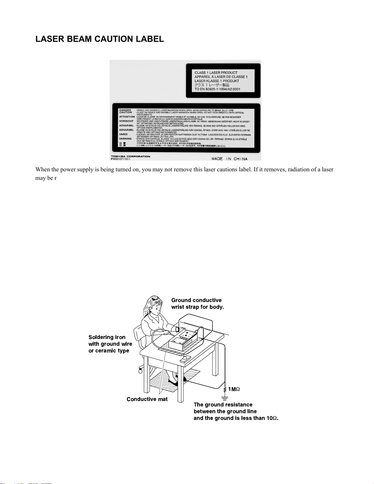
LASER BEAM CAUTION LABEL
When the power supply is being turned on, you may not remove this laser cautions label. If it removes, radiation of a laser
may be received.
PREPARATION OF SERVICING
Pickup Head consists of a laser diode that is very susceptible to external static electricity.
Although it operates properly after replacement, if it was subject to electrostatic discharge during replacement,
its life might be shortened. When replacing, use a conductive mat, soldering iron with ground wire, etc. to
protect the laser diode from damage by static electricity.
And also, the LSI and IC are same as above.
Ground conductive
wrist strap for body.
Soldering iron
with ground wire
or ceramic type
1M
W
Conductive mat
The ground resistance
between the ground line
and the ground is less than 10W.
SAFETY NOTICE
SAFETY PRECAUTIONS
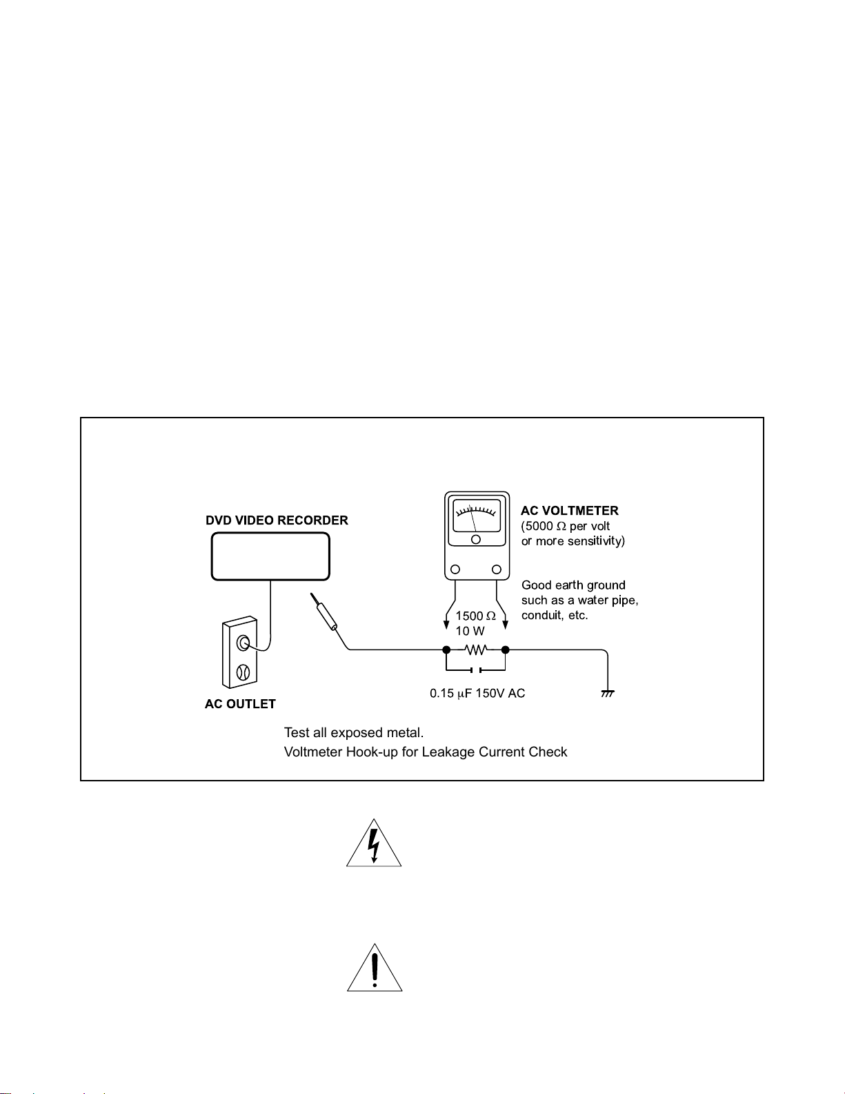
LEAKAGE CURRENT CHECK
Plug the AC line cord directly into a 120V AC outlet (do
not use an isolation transformer for this check). Use an
AC voltmeter, having 5000 W per volt or more sensitivity.
Connect a 1500 W 10 W resistor, paralleled by a 0.15 mF
150V AC capacitor between a known good earth ground
(water pipe, conduit, etc.) and all exposed metal parts of
cabinet (antennas, handle bracket, metal cabinet
screwheads, metal overlays, control shafts, etc.).
READING SHOULD NOT EXCEED 0.3V
Measure the AC voltage across the 1500 W resistor.
The test must be conducted with the AC switch on and
then repeated with the AC switch off. The AC voltage
indicated by the meter may not exceed 0.3 V. A reading
exceeding 0.3 V indicates that a dangerous potential
exists, the fault must be located and corrected.
Repeat the above test with the DVD VIDEO RECORDER
power plug reversed.
NEVER RETURN A DVD VIDEO RECORDER TO
THE CUSTOMER WITHOUT TAKING NECESSARY
CORRECTIVE ACTION.
DVD VIDEO RECORDER
AC OUTLET
Test all exposed metal.
Voltmeter Hook-up for Leakage Current Check
AC VOLTMETER
(5000Wper volt
or more sensitivity)
Good earth ground
such as a water pipe,
W
conduit, etc.
1500
10 W
0.15mF 150V AC
The lightning flash with arrowhead symbol, within an
equilateral triangle, is intended to alert the user to the
presence of uninsulated “dangerous voltage” within the
product’s enclosure that may be of sufficient magnitude to
constitute a risk of electric shock to persons.
The exclamation point within an equilateral triangle is
intended to alert the user to the presence of important
operating and maintenance (servicing) instructions in the
literature accompanying the appliance.

1. OPERATING INSTRUCTIONS
CONTENTS
SECTION 1
GENERAL DESCRIPTIONS
2. LOCATION OF MAIN PARTS
2-1. Location of Main Parts
2-2. Location of PC Boards
1. Replacement of Mechanical Parts
1-1. Cabinet Replacement
1-1-1. Top Cover
1-1-2. Front Panel
1-1-3. Tray Door
1-1-4. Operation Panel Door
1-1-5. RAM Diver
1-1-6. Fan
1-1-7. Rear Panel
1. CIRCUIT SYMBOLS AND
SUPPLEMENTARY EXPLANATION
1-1. Precautions for Part Replacement
1-2. Solid Resistor Indication
1-3. Capacitance Indication
1-4. Inductor Indication
1-5. Waveform and Voltage Measurement
1-6. Others
2. PRINTED WIRING BOARD AND
SCHEMATIC DIAGRAM
3. BLOCK DIAGRAMS
3-1. Overall Block Diagram
4. CIRCUIT DIAGRAMS
4-1. Power Supply Circuit Diagram
4-2. Front Circuit Diagram
4-2-1. Front Jack Circuit Diagram
4-2-2. Front Circuit Diagram (L)
4-2-3. Front Circuit Diagram (R)
PART REPLACEMENT AND ADJUSTMENT PROCEDURES
SECTION 2
1-2. PC Board Replacement
1-2-1. Digital PC Board
1-2-2. Mother PC Board
1-2-3. Power PC Board
1-2-4. Front (R), Front (L), Front (Jack) PC Board
SECTION 3
SERVICING DIAGRAMS
4-3. Digital Circuit Diagram
4-3-1. Digital 1 Circuit Diagram
4-3-2. Digital 2 Circuit Diagram
4-4. Mother Circuit Diagram
4-4-1. Tuner Circuit Diagram
4-4-2. Timer Circuit Diagram
4-4-3. Audio Circuit Diagram
4-4-4. Video Circuit Diagram
5. PC BOARDS
5-1. Front Jack PC Board
5-2. Front (L) PC Board
5-3. Front (R) PC Board
5-4. Digital PC Board
5-5. Mother PC Board
SAFETY PRECAUTION
NOTICE
ABBREVIATIONS
1. Integrated Circuit (IC)
2. Capacitor (Cap)
3. Resistor (Res)
SECTION 4
PARTS LIST
4. EXPLODED VIEWS
4-1. Packing Assembly
4-2. Chassis Assembly
5. PARTS LIST

GENERAL DESCRIPTIONS
SECTION 1
GENERAL DESCRIPTIONS
1. OPERATING INSTRUCTIONS
Please refer to the owner's manual about the contents.
SECTION 1
2. LOCATION OF MAIN PARTS
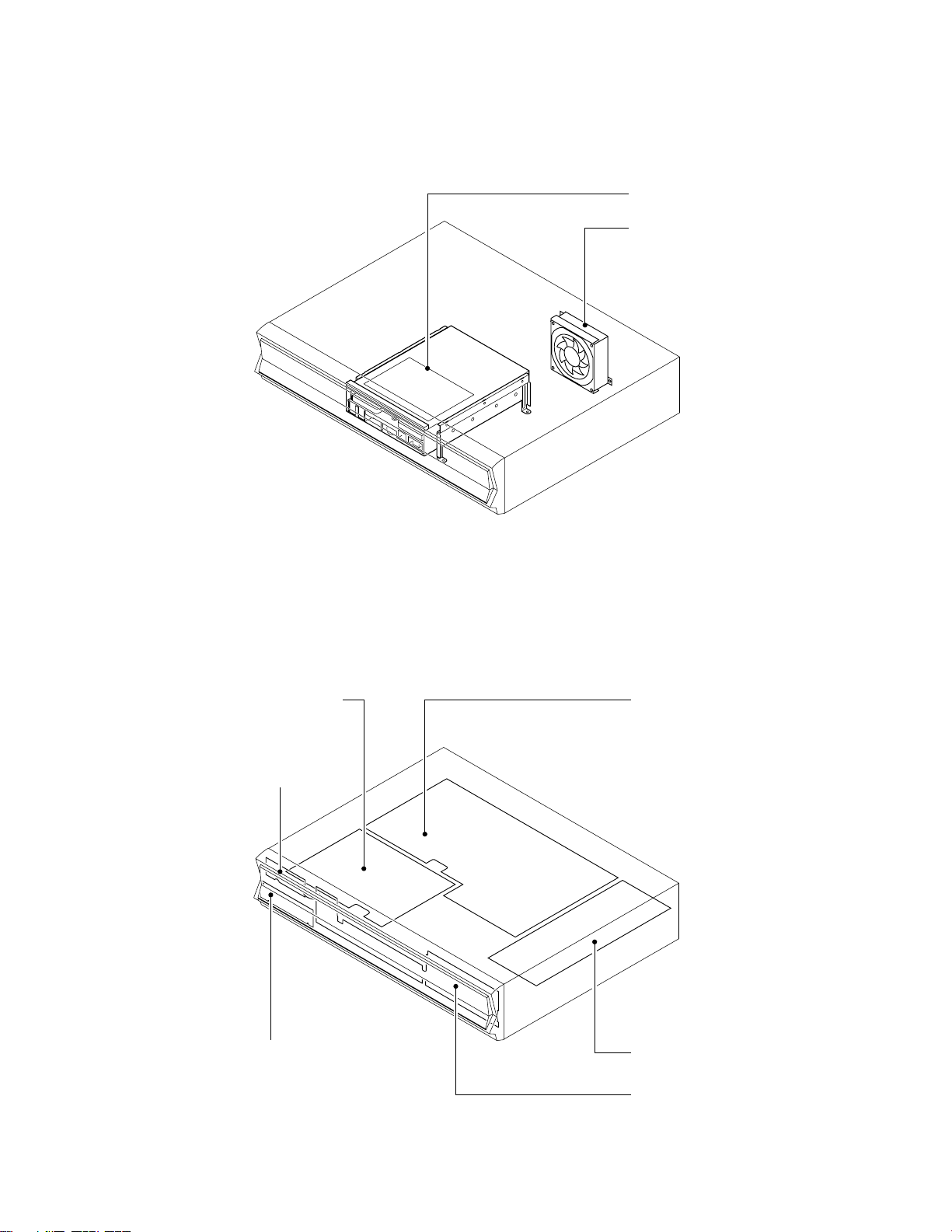
2-1. Location of Main Parts
RAM1 RAM DRIVE
ZG45 FAN
2-2. Location of PC Boards
EU01 Digital PC Board
EU03B Front (L)
PC Board
Fig. 1-2-1
EU05 Mother PC board
EU55 Front (Jack) PC Board
EU02 Power PC board
EU03A Front (R) PC Board
Fig. 1-2-2
SECTION 2
PART REPLACEMENT AND
ADJUSTMENT PROCEDURES
CAUTIONS BEFORE STARTING PART REPLACEMENT
Electronic parts are susceptible to static electricity and may easily damaged, so do not forget to ground as required.
Many screws are used inside the unit. To prevent the screws from missing or dropping, etc. always use a magnetized
screwdriver in servicing. Several kinds of screws are used and some of them need special cautions. That is, take care of
the tapping screws securing molded parts and fine pitch screws used to secure metal parts. If they are used improperly,
the screw holes will be easily damaged and the parts can not be fixed.
1. REPLACEMENT OF MECHANICAL PARTS
ADJUSTMENT PROCEDURES
PART REPLACEMENT AND
1-1. Cabinet Replacement
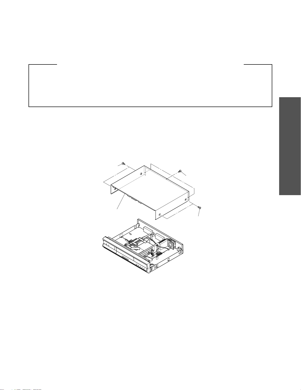
1-1-1. Top Cover
1. Remove seven screws (1), then remove the top cover (2).
Screws (1)
Top cover (2)
SECTION 2
Screws (1)
Screws (1)
Fig. 2-1-1
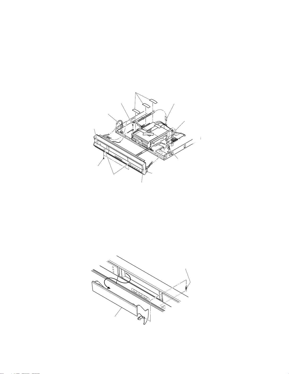
1-1-2. Front Panel
1. Remove the top cover. (Refer to item 1-1-1.)
2. Peel off three tapes (1) and disconnect the flexible cable (2).
3. Disconnect the flexible cable (3) and two connectors (4).
4. Remove the screw (5).
5. Remove two screws (6).
6. Release four claws, then remove the front panel (7).
Tapes (1)
Screw (5)
Connector (4)
Claw
Screws (6)
Claws
Front panel (7)
Flexible cable (2)
Claw
Fig. 2-1-2
1-1-3. Tray Door
1. Remove the front (R) PC board and front (L) PC board. (Refer to item 1-2-4.)
2. Remove the spring (1).
3. Remove the tray door (2) while slightly bending it.
Flexible
cable (3)
Connector (4)
Tray door (2)
Spring (1)
Fig. 2-1-3
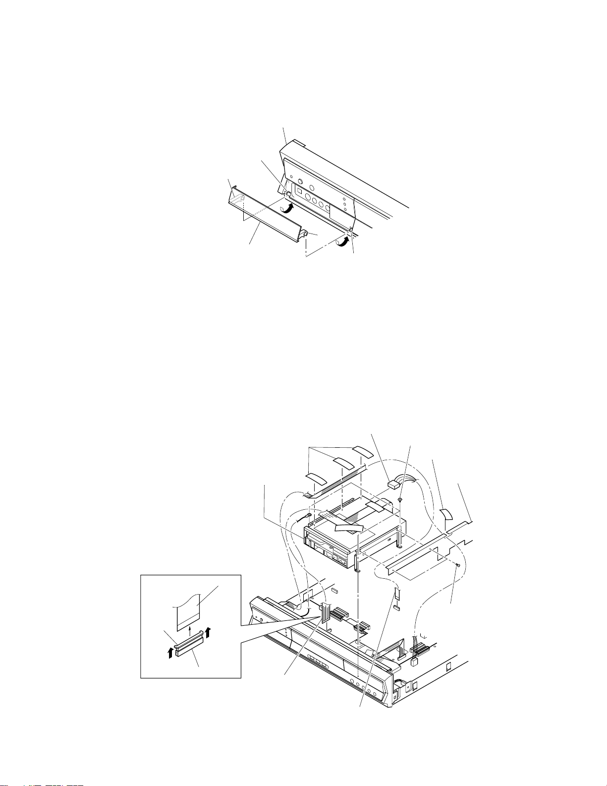
1-1-4. Operation Panel Door
1. Open the operation panel door (1).
2. Release two claws and unhinge the door (1).
Front panel
Hinge
Claw
Operation panel door (1)
Fig. 2-1-4
1-1-5. RAM Drive
1. Peel off four tapes (1).
2. Disconnect two flexible cables (2).
3. Disconnect the connector (3).
4. Remove two screws (4) and acrylic board (5).
5. Remove four screws (6), then remove the RAM drive (7).
Claw
Hinge
Flexible cable (2)
Claw
A
Remove the connector claw
in the direction indicated
by the arrows to release the
flexible cable.
A
Connector
Tapes (1)
RAM drive (7)
Flexible cable (2)
Connector (3)
Screws (6)
Tape (1)
Acrylic
board (5)
Screws (4)
Flexible
cable (2)
Fig. 2-1-5
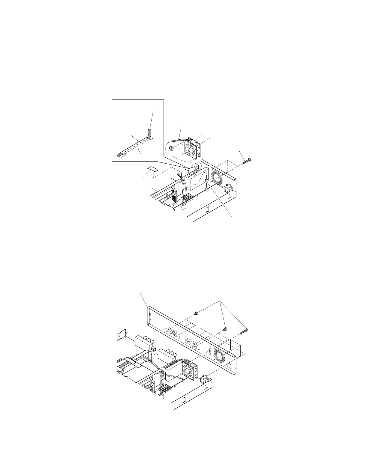
1-1-6. Fan
1. Peel off the tape (1).
2. Disconnnect the connector (2).
3. Remove four screws (3) and the fan (4).
Note:
• After replacing the fan (4), attatch the tape (1) as it was.
Wire (5)
Pass the wire (5)
underneath the
folded part.
Acrylic board
Tape (1)
Wire (5)
Fig. 2-1-6
1-1-7. Rear Panel
1. Remove twelve screws (1), then remove the rear panel (2).
Rear panel (2)
Fan (4)
Screws (3)
Connector (2)
Screws (1)
Fig. 2-1-7
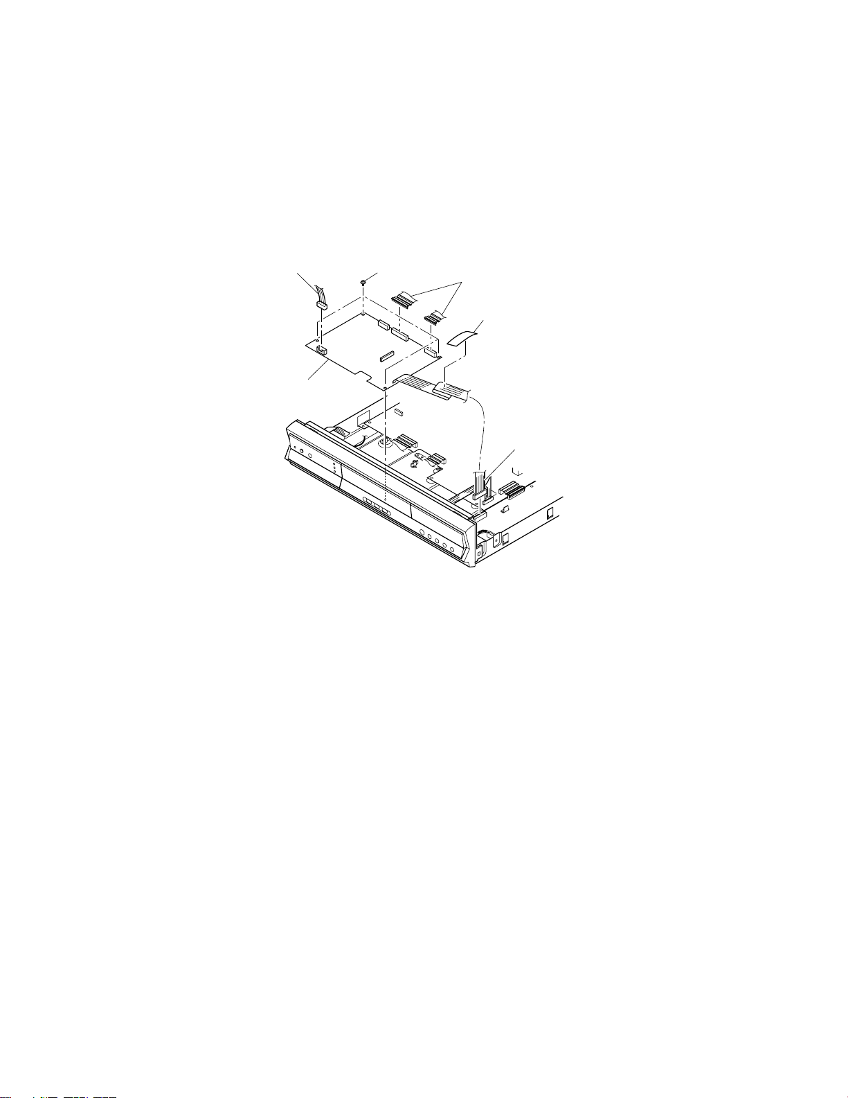
1-2. PC Board Replacement
1-2-1. Digital PC Board
1. Remove the RAM drive. (Refer to 1-1-5.)
2. Disconnect two connectors (1).
3. Peel off the tape (2), then disconnect the connector (3).
4. Disconnect the connector (4).
5. Remove four screws (5) and the digital PC board (6).
Connector (4)
Digital PC
board (6)
Screws (5)
Connectors (1)
Tape (2)
Connector (3)
Fig. 2-1-8
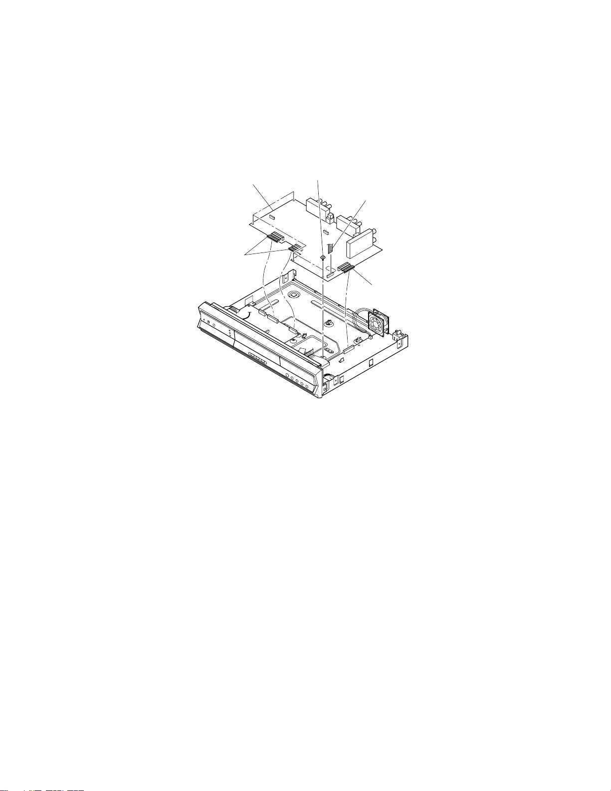
1-2-2. Mother PC Board
1. Remove the RAM drive. (Refer to item 1-1-5.)
2. Remove the rear panel. (Refer to item 1-1-7.)
3. Disconnect three connectors (1).
4. Disconnect the flexible cable (2).
5. Remove four screws (3), then remove the mother PC board (4).
Mother PC board (4)
Connectors (1)
Screws (3)
Flexible cable (2)
Connector (1)
Fig. 2-1-9
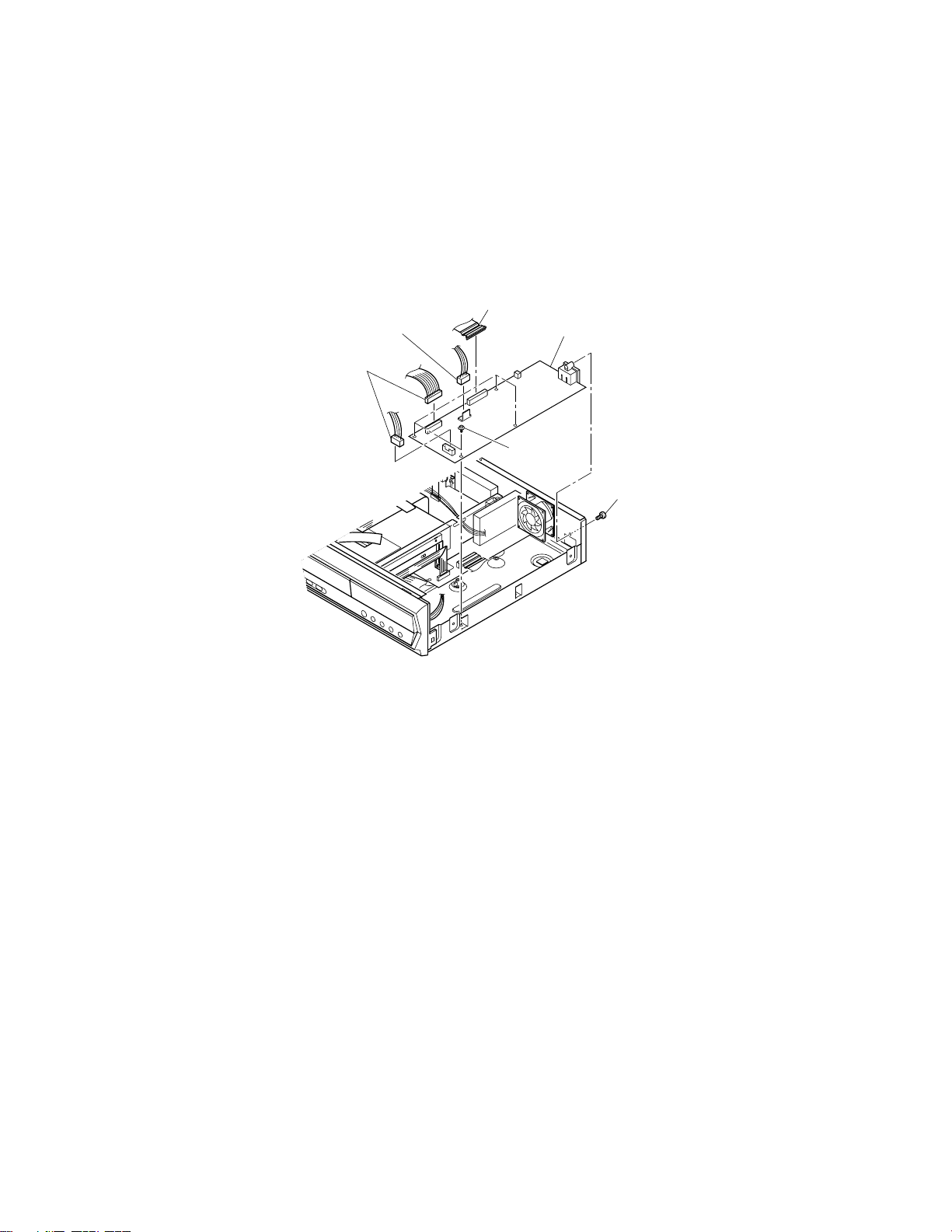
1-2-3. Power PC Board
Cautions :
• Danger of explosion if battery is incorrectly replaced.
• Replace only with the same or equivalent type.
1. Disconnect three connectors (1).
2. Disconnect the connector (2).
3. Remove the screw (3), four screws (4) and the power PC board (5).
Connector (2)
Connector (1)
Connectors (1)
Power PC board (5)
Screws (4)
Screw (3)
Fig. 2-1-10
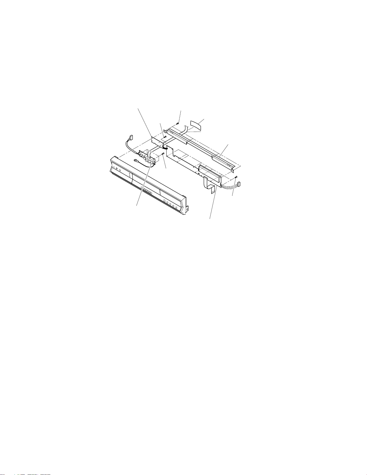
1-2-4. Front (R), Front (L), Front (Jack) PC Board
1. Remove the front panel. (Refer to item 1-1-2.)
2. Disconnect the flexible cable (1), then peel off the tape (2).
3. Remove four screws (3), then remove the stay (4).
4. Remove eight screws (5) and the screw (6), then remove the front (R) PC board (7) and front (L) PC board (8).
5. Remove four screws (9), then remove the front (Jack) PC board (10).
Front (L) PC board (8)
Screw (6)
Front (Jack)
PC board (10)
Screws (3)
Tape (2)
Flexible cable (1)
Stay (4)
Screws (9)
Screws (5)
Front (R) PC board (7)
Fig. 2-1-11
+
NP
104
10x10
4
pF (0.1mF)
Temperature characteristic
(or Temperature characteristic+
Static electricity capacity tolerance)
SECTION 3
SERVICING DIAGRAMS
1. CIRCUIT SYMBOLS AND SUPPLEMENTARY EXPLANATION
1-1. Precautions for Part Replacement
• In the schematic diagram, parts marked (ex.
F801) are critical part to meet the safety regulations,
so always use the parts bearing specified part codes
(SN) when replacing them.
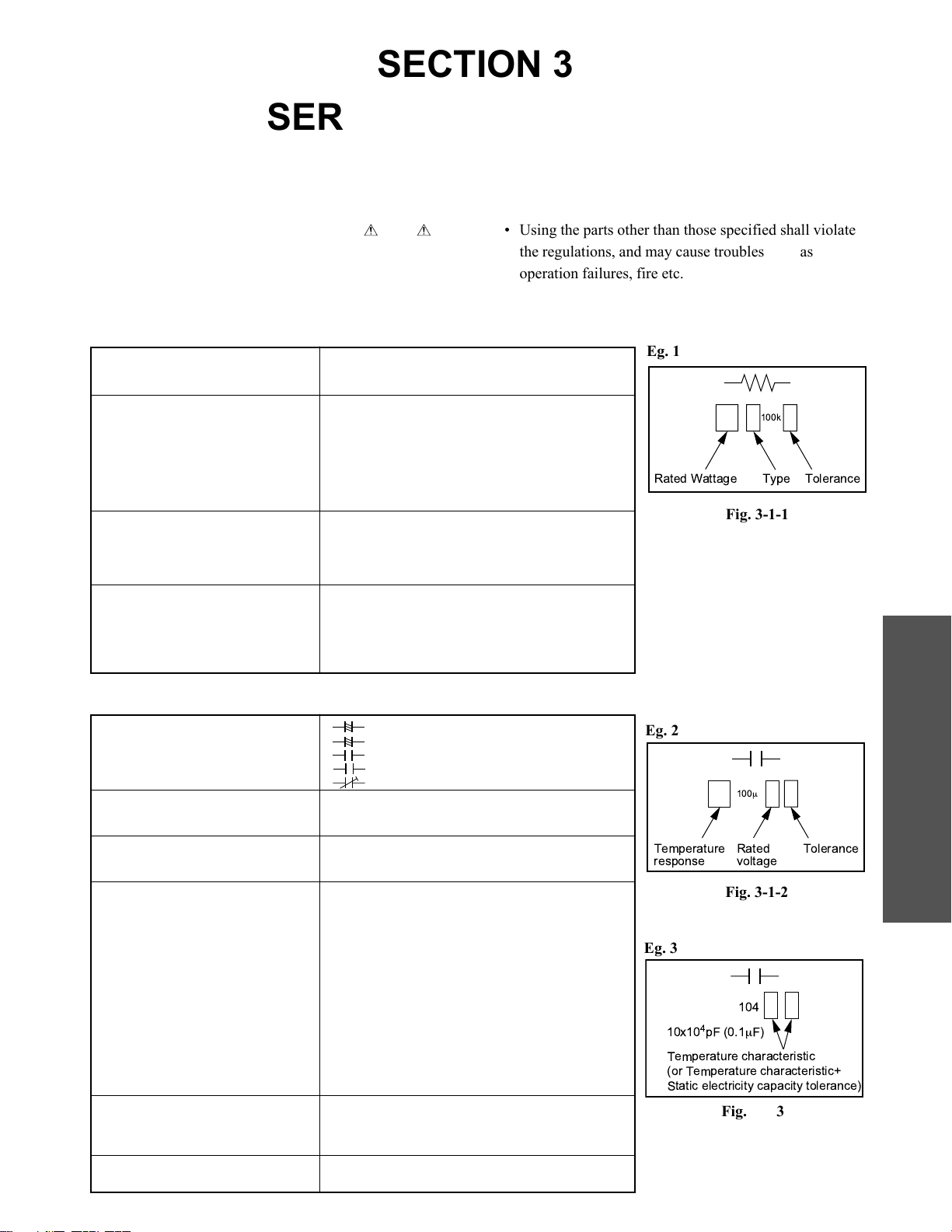
1-2. Solid Resistor Indication
Unit None ........... W
K ........... kW
M ........... MW
Tolerance None ........... ±5%
B ........... ±0.1%
C ........... ±0.25%
D ........... ±0.5%
F ........... ±1%
G ........... ±2%
K ........... ±10%
M ........... ±20%
Rated Wattage (1) Chip Parts
None ......... 1/16W
(2) Other Parts
None ......... 1/6W
Other than above, described in the Circuit Diagram.
Type None ........... Carbon film
S ........... Solid
R ........... Oxide metal film
M ........... Metal film
W ...........Cement
FR ........... Fusible
• Using the parts other than those specified shall violate
the regulations, and may cause troubles such as
operation failures, fire etc.
Eg. 1
100k
Rated Wattage Type Tolerance
Fig. 3-1-1
SERVICING DIAGRAMS
1-3. Capacitance Indication
Symbol
Unit None ........... F
Rated voltage None ........... 50V
Tolerance (1) Ceramic, plastic, and film capacitors of which
Temperature characteristic None ........... SL
(Ceramic capacitor) For others, temperature characteristics are
Static electricity capacity Sometimes described with abbreviated letters as
(Ceramic capacitor) shown in Eg. 3.
........... Electrolytic, Special electrolytic
........... Non polarity electrolytic
........... Ceramic, plastic
M
........... Film
........... Trimmer
m ........... mF
p ........... pF
For other than 50V and electrolytic capacitors,
described in the Circuit Diagram.
capacitance are more than 10 pF.
None ........... ±5% or more
B ........... ±0.1%
C ........... ±0.25%
D ........... ±0.5%
F ........... ±1%
G ........... ±2%
(2) Ceramic, plastic, and film capacitors of which
capacitance are 10 pF or less.
None ........... more than ±5 pF
B ........... ±0.1 pF
C ........... ±0.25 pF
(3) Electrolytic, Trimmer
Tolerance is not described.
described. (For capacitors of 0.01 mF and
no indications are described as F.)
Eg. 2
Temperature
response
Eg. 3
100
m
Rated
voltage
Fig. 3-1-2
Fig. 3-1-3
SECTION 3
Tolerance
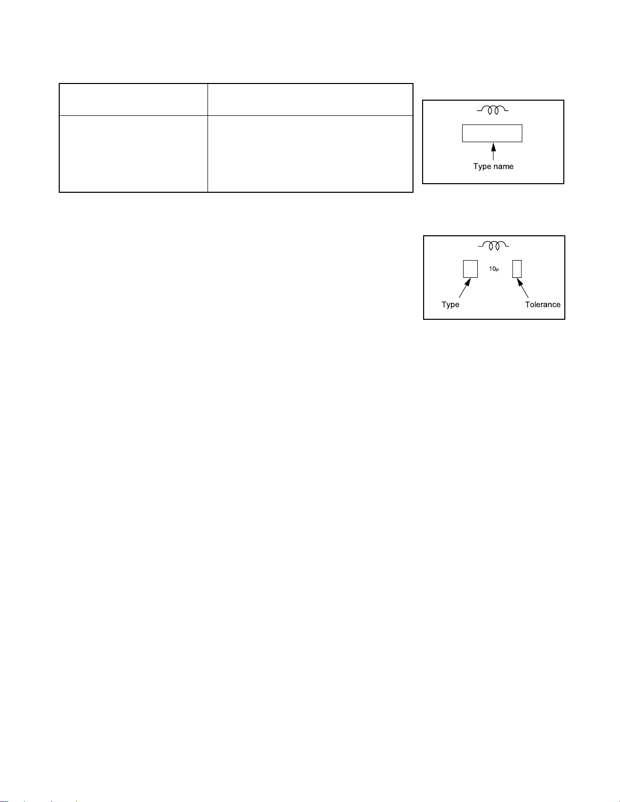
1-4. Inductor Indication
Type name
10
m
Type Tolerance
Unit None ........... H
m ........... mH
m ...........mH
Tolerance None ........... ±5%
B ........... ±0.1%
C ........... ±0.25%
D ........... ±0.5%
F ........... ±1%
G ........... ±2%
K ........... ±10%
M ........... ±20%
1-5. Waveform and Voltage Measurement
• The waveforms for CD/DVD and RF shown in the
circuit diagrams are obtained when a test disc is
played back.
• All voltage values except the waveforms are expressed
in DC and measured by a digital voltmeter.
1-6. Others
• The parts indicated with "NC" or "KETU" etc. are not
used in the circuits of this model.
Eg. 4
Fig. 3-1-4
Eg. 5
Fig. 3-1-5
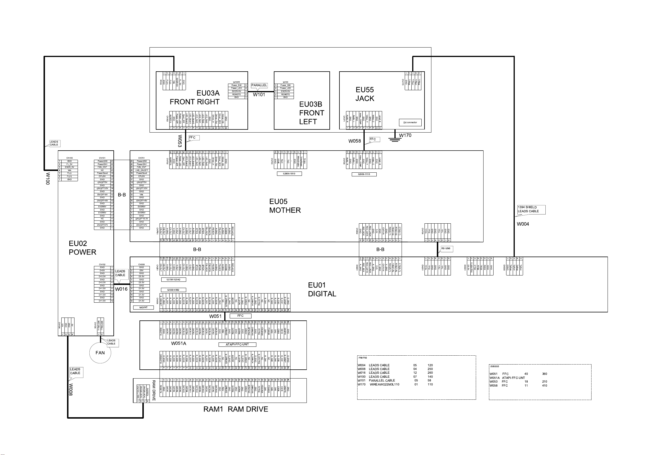
2. PRINTED WIRING BOARD AND SCHEMATIC DIAGRAM
LEADS
CABLE
CN105
GND
7 23
FL_5V
6 22
EVER_5V
5 21
Vkk NC
4 20
W100
3 19
FL(-)
FL(+)
2 18
GND
1 17
CN101
PowerON0
PowerON1
FAN_CNT
PowerGood
CPU5V
GND
ON/OFF5V
GND
ON/OFF3.0V
GND
ON/OFF-9V
GND
ON/OFF+9V
GND
EVER6V
GND
EVER6V
GND
NC
GND
ON/OFF37V
GND
23
22
21
20
19
18
17
16
15 15
14 14
13 13
12 12
B-B
11 11
10 10
9
8
7
6
5
4
3
2
1
16
9
8
7
6
5
4
3
2
1
CN701
PowerON0
PowerON1
FAN_CNT
LNB_ON/OFF
PowerGood
CPU5V
GND
ON/OFF5V
GND
ON/OFF3.0V
GND
Vkk
GND
ON/OFF+9V
GND
EVER6V
GND
EVER6V
GND
ON/OFF15.3V
GND
ON/OFF37V
GND
1234567
EVER+5V
W100
FL_5V
FL(+)
FL(-)
GND
GND
Vkk
FRONT RIGHT
Power_LED
LED_Scan2
Power_SW
Eject_SW
REMOTE
CN102
GND
123456789
W053
181716151413121110
LED_Scan2
Power_LED
Power_SW
Eject_SW
REMOTE
CN702
GND
CR-OUT
CB-OUT
CY-OUT
CNW01
CV-OUT
V-GND
V-GND
V-GND
V-GND
Y-OUT
EU03A
LED_Scan1
LED_Scan0
LED_Out3
LED_Out1
101112131415161718
FFC
987654321
LED_Scan1
LED_Scan0
LED_Out3
LED_Out1
A-GND
C-OUT
SPICS
SPIDA
12345
CN170
TPAop
TPAon
TPBon
TPBop
W100R W150
5
Power_SW
EVER+5V
REMOTE
GND
4
3
2
1
PARALLEL
W101
5
4
3
2
1
Power_SW
Power_LEDPower_LED
EVER+5V
REMOTE
GND
EU55
JACK
GND
EU03B
Driver_SCK
Driver_Out
LED_Out2
Driver_CS
LED_Out0
Driver_In
GND
GND
FRONT
LEFT
10
Driver_SCK
Driver_Out
LED_Out2
Driver_CS
LED_Out0
Driver_In
GND
GND
987654321
CN703
EE40
GND
RxD
-
52806-1010
WriteEnable
TimerReset
5vcpu
GND
TxD
-
EU05
MOTHER
PB-LRCK
PB-DATA
PB-BCK
SPICK
REC-ACK
PB-ACK
IEC958
A-GND
A-GND
A-GND
Video_COMP
Audio_R
Audio_L
CN171
GND
GND
123456789
W058
11
10
987654321
Video_COMP
Audio_R
Audio_L
CN704
GND
GND
52806-1110
CN902
GND
Video_C
Video_Y
Line2_S
GND
GND
GND
10
11
FFC
Video_C
Video_Y
Line2_S
GND
GND
GND
REC_DATA
REC_LRCK
REC_BCK
CV/Y-IN
GND
GND
GND
C-IN
DV connector
W170
1394 SHIELD
LEADS CABLE
RXD(E-T)
TXD(T-E)
RTS(T-E)
CTS(E-T)
CN706
TPO+
TPO-
GND
GND
GND
GND
TPI+
TPI-
W004
EU02
POWER
CN104
GND
GND
12V
5V
123
4
LEADS
CABLE
W008
CN106
FAN
CN102
D+3.3V
D+3.3V
D+1.5V
D+1.5V
D+1.5V
MOTOR(+)
1
GND
D+5V
GND
GND
GND
GND
GND
MOTOR(-)
2
1
2
LEADS
3
CABLE
4
5
6
7
8
W016
9
10 10
11 11
12 12
LEADS
CABLE
23222120191817161514131211
23222120191817161514131211
CR-OUT
CB-OUT
CY-OUT
CV-OUT
V-GND
V-GND
V-GND
CN508
GND
1
D5V
2
GND
3
D3.3V
4
GND
5
D3.3V
6
GND
7
D1.5V
8
GND
9
D1.5V
GND
D1.5V
MOUNT
CN506CNZ01
Y-OUT
127301123K2
52559-4082
B_DRESET
D_GND
B_DD8
B_DD6
B_DD9
B_DD5
B_DD7
123456789
123456789
RESETX
DATA6
DATA9
DATA5
DATA7
DATA8
GND
B_DD10
DATA10
W051A
12V(YELLOW)
123
GND(BLACK)
GND(BLACK)
5V(RED)
4
DRESETB
D_GND
123456789
123456789
RAM DRIVE
RESETX
GND
B_DD10
B_DD7
B_DD8
B_DD6
B_DD9
B_DD5
DATA10
DATA7
DATA8
DATA6
DATA9
DATA5
10
987654321
B-B
10
987654321
PB-LRCK
PB-DATA
V-GND
A-GND
C-OUT
B_DD11
B_DD4
B_DD3
10111213141516171819202122232425262728293031323334353637383940
10111213141516171819202122232425262728293031323334353637383940
DATA11
DATA4
DATA3
B_DD11
B_DD4
B_DD3
10111213141516171819202122232425262728293031323334353637383940
10111213141516171819202122232425262728293031323334353637383940
DATA11
DATA4
DATA3
PB-BCK
SPICS
SPIDA
SPICK
B_DD14
B_DD12
B_DD13
B_DD1
B_DD2
B_DD0
W051
DATA13
DATA14
DATA12
DATA0
DATA2
DATA1
B_DD12
B_DD13
B_DD14
B_DD2
B_DD1
B_DD0
DATA12
DATA13
DATA14
DATA2
DATA1
DATA0
PB-ACK
A-GND
A-GND
B_DD15
D_GND
NC
DATA15
GND
RSV
B_DD15
D_GND
NC
DATA15
GND
RSV
REC-ACK
IEC958
A-GND
B_DMAREQ
B_DIOR
BDIOW
D_GND
D_GND
NC
FFC
DMARQ
DIOWX
DIORX
GND
GND
GND
ATAPI-FFC-UNT
B_DMARQ
B_DIOR
BDIOW
D_GND
D_GND
NC
DMARQ
DIOWX
DIORX
GND
GND
GND
B_IORDY
IORDY
B_IORDY
IORDY
B_DMACK
NC
DMACKX
SPSYNC
B_DMACK
NC
DMACKX
SPSYNC
B_INTRQ
D_GND
B_DA0
B_DA1
B_CS2
B_CS0
NC
NC
IOCS16X
PDIAGX
INTRQ
GND
B_DINTRQ
D_GND
INTRQ
GND
NC
IOCS16X
DA1
B_DA1NCB_DA0
PDIAGX
DA1
CS0X
DA0
DA2
B_DA2
B_CS0
CS0X
DA0
DA2
131211
10
CN401
131211
A_GND
987654321
10
987654321
REC_DATA
REC_LRCK
REC_BCK
A_GND
B-B
V_GND
C-IN
RXD(R-T)
TXD(T-R)
RTS(T-R)
CTS(R-T)
CV/Y-IN
V_GND
1234567
1234567
CN201
TPO+
TPO-
GND
8
no use
8
GND
TPI+
GND
GND
TPI-
1234567
FLSSHW-X
CN501
D3.3V
CTS2
8
12345
CN500
TpAon
TpBop
TpBon
DGND
RXD2
TXD2
RTS2
GND
GND
TpAop
EU01
B_DASP
D_GND
B_CS1 CS1X
DASPX
GND
B_DASP
D_GND
B_CS1
DASPX
CS1X
GND
DIGITAL
memo
W004 LEADS CABLE 05 120
W008 LEADS CABLE 04 250
W016 LEADS CABLE 12 260
W100 LEADS CABLE 07 140
W101 PARALLEL CABLE 05 58
W170 WIREAWG22M3L110 01 110
memo
W051 FFC 40 360
W051A ATAPI-FFC-UNT
W053 FFC 18 210
W058 FFC 11 410
RAM1 RAM DRIVE
Fig. 3-2-1
 Loading...