Page 1
FILE NO. 810-200559
SERVICE MANUAL
DVD RECORDER
D-R250SB
D-R255SF
D-R255SG
JUL. 2005 S
Page 2
8-1
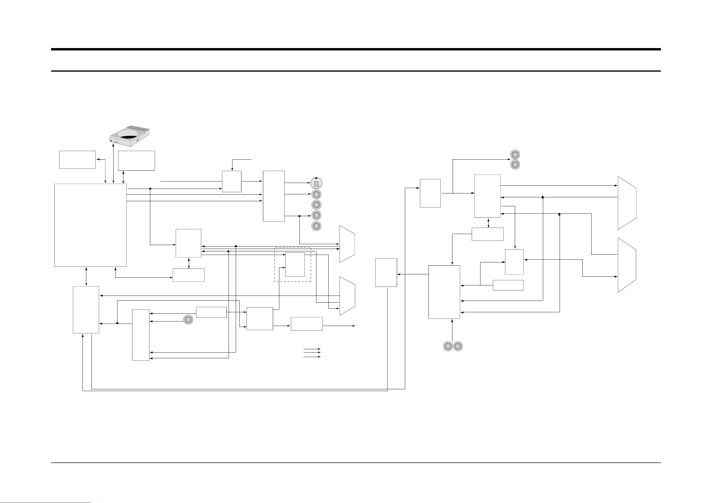
8. Block Diagram
4MB FLASH
AM290L323GB
(2Mx 16bit)
MPEG-2
A/V CODEC
Video
Decoder
64MB DDR-SDRAM
K4H561638F-TCB3
(16Mx 16bitx2wa)
RGB
CVBS/Y
mux
CVBS
RF
AV3
OSD
CVBS
NM1647
Front Micom
RF Tuner
NM1501
OSD_SEL
NJM 2267
(6dB AMP)
NM1623
MM1501
VPS/Sync
Detector
S-Video 1
Video 1
Component
OSD
SCART1 (TV)
SCART2 (EXT)
Audio
ADC
Audio
DAC
Tuner
EXT1
mux
BD3824
L/R
EXT2
EXT3
Front
NOM1647
Front Micom
BU4052
RF Tuner
mux
AV OUT (L/R)
SCART1 (TV)
SCART2 (EXT)
AVI (L/R)
AV2 (L/R)
(A/I)
AV1 (CVBS)
AV2 (CVBS)
RGB
V/C
CVBS
AV3 (L/R)
Page 3
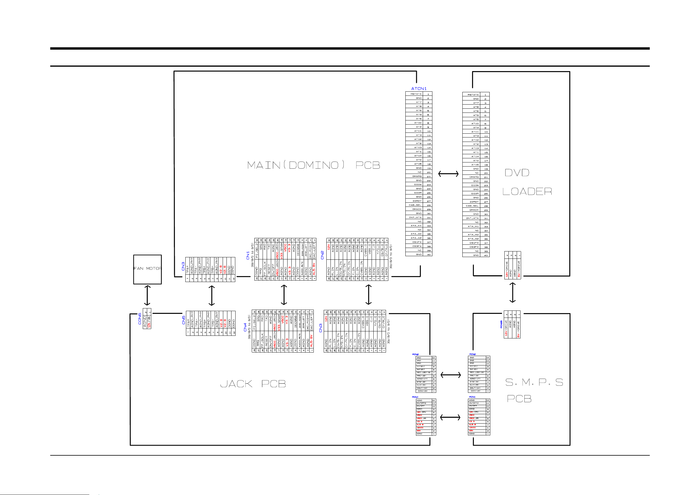
9. Wiring Diagram
9-1
Page 4
Schematic Diagrams
11-2
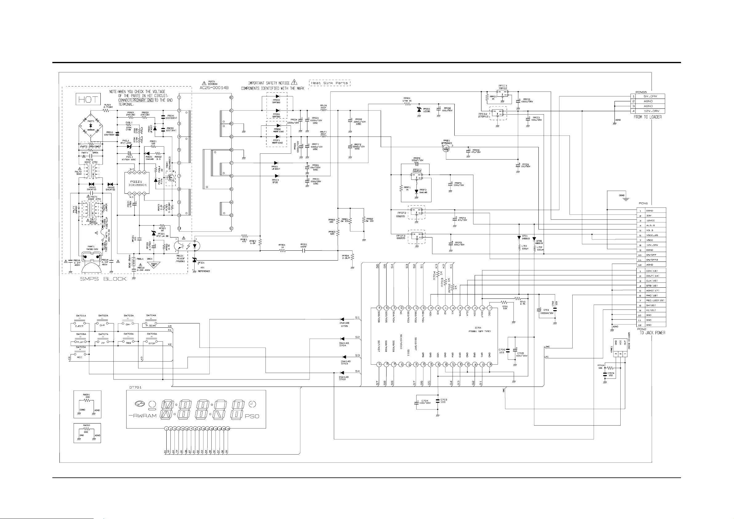
11-1 S.M.P.S. (SMPS PCB)
Page 5
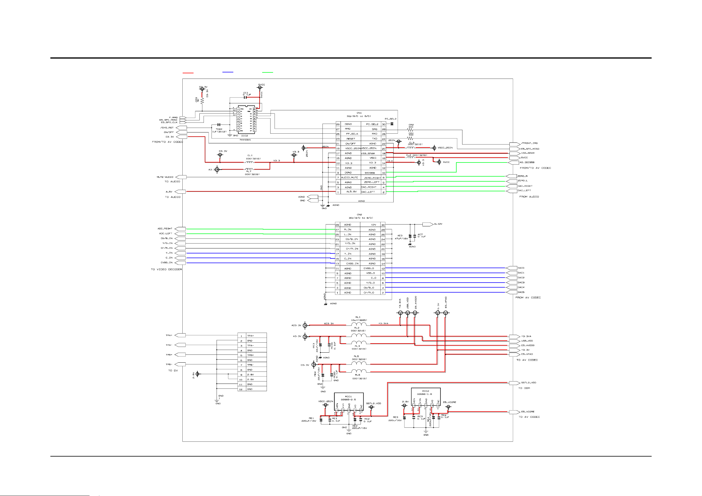
Schematic Diagrams
11-3
11-2 Main Connector (DVD PCB)
Power
Video
Audio
Page 6
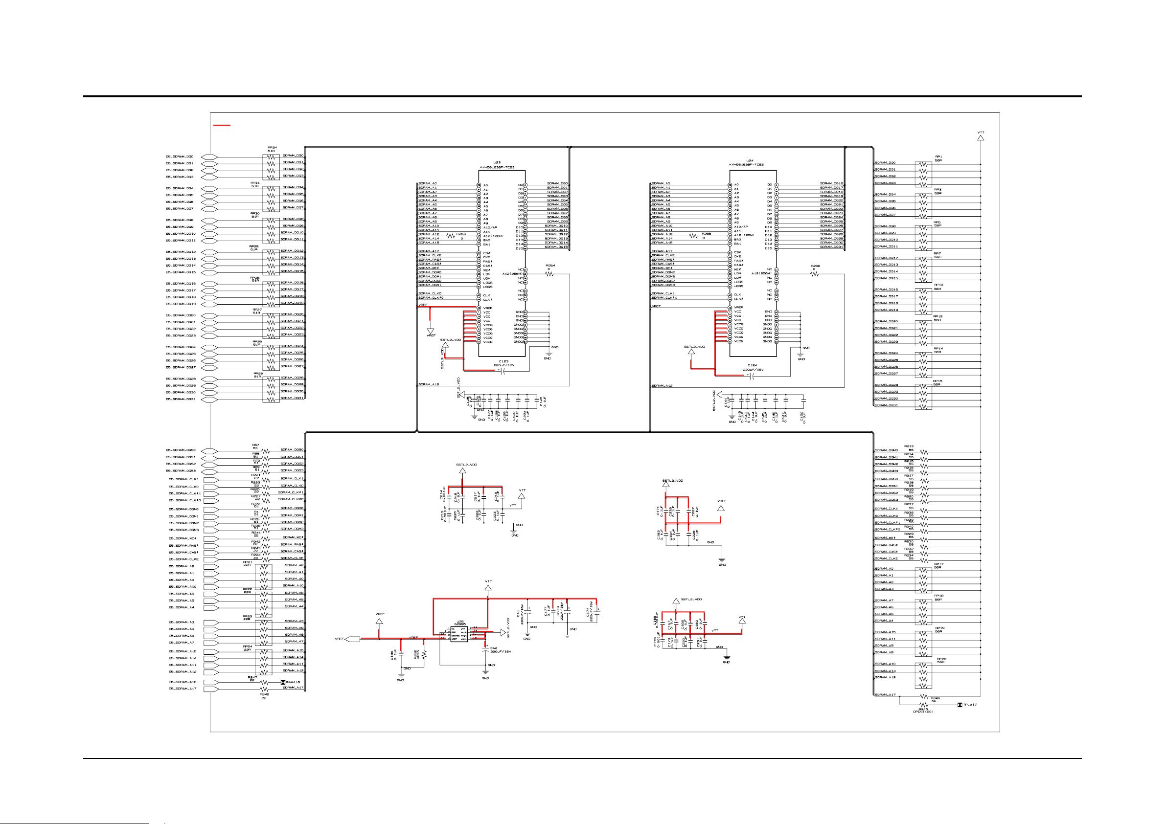
Schematic Diagrams
11-4
11-3 DDR (DVD PCB)
Power
Page 7
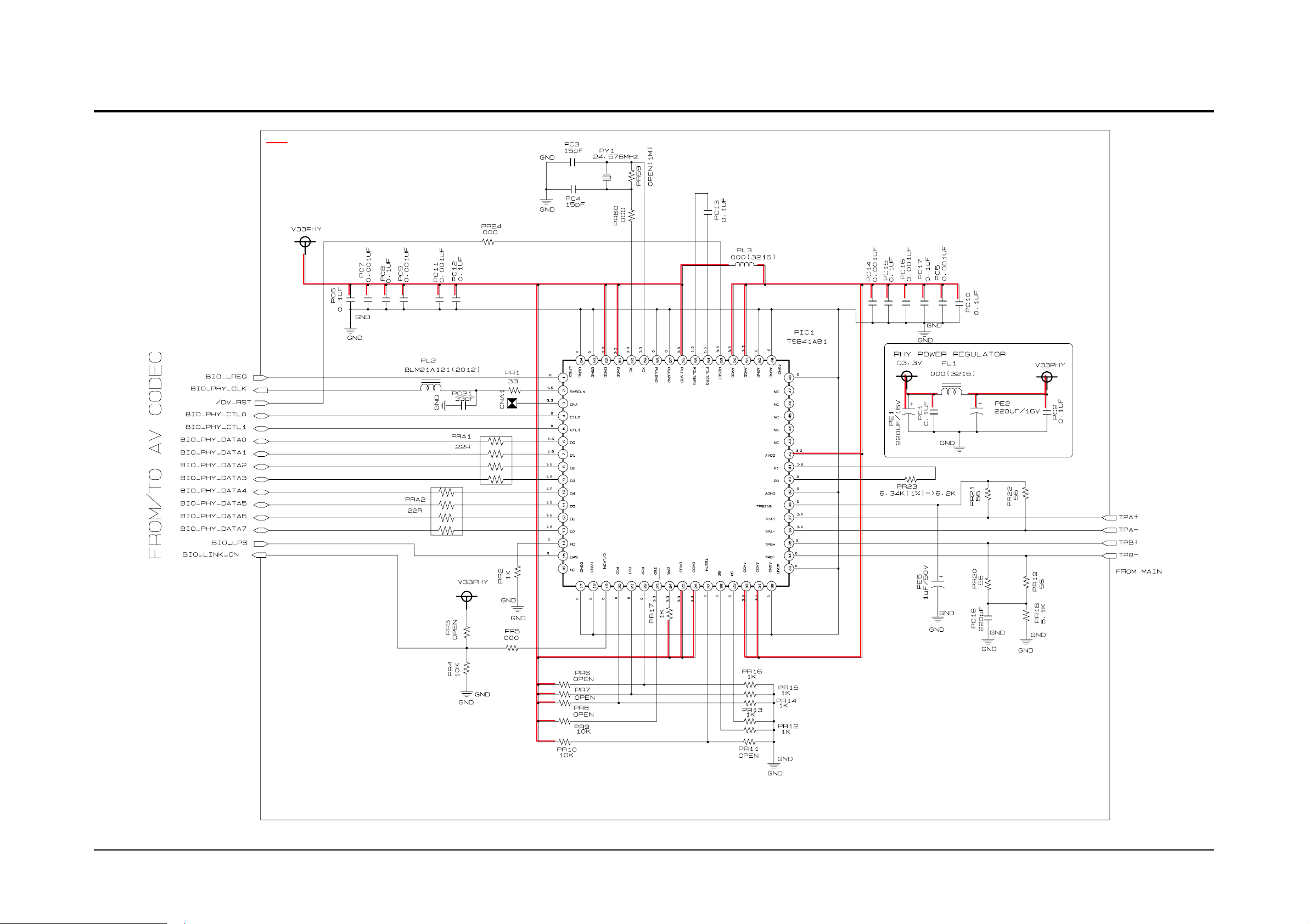
Schematic Diagrams
11-5
11-4 DV (DVD PCB)
Power
Page 8
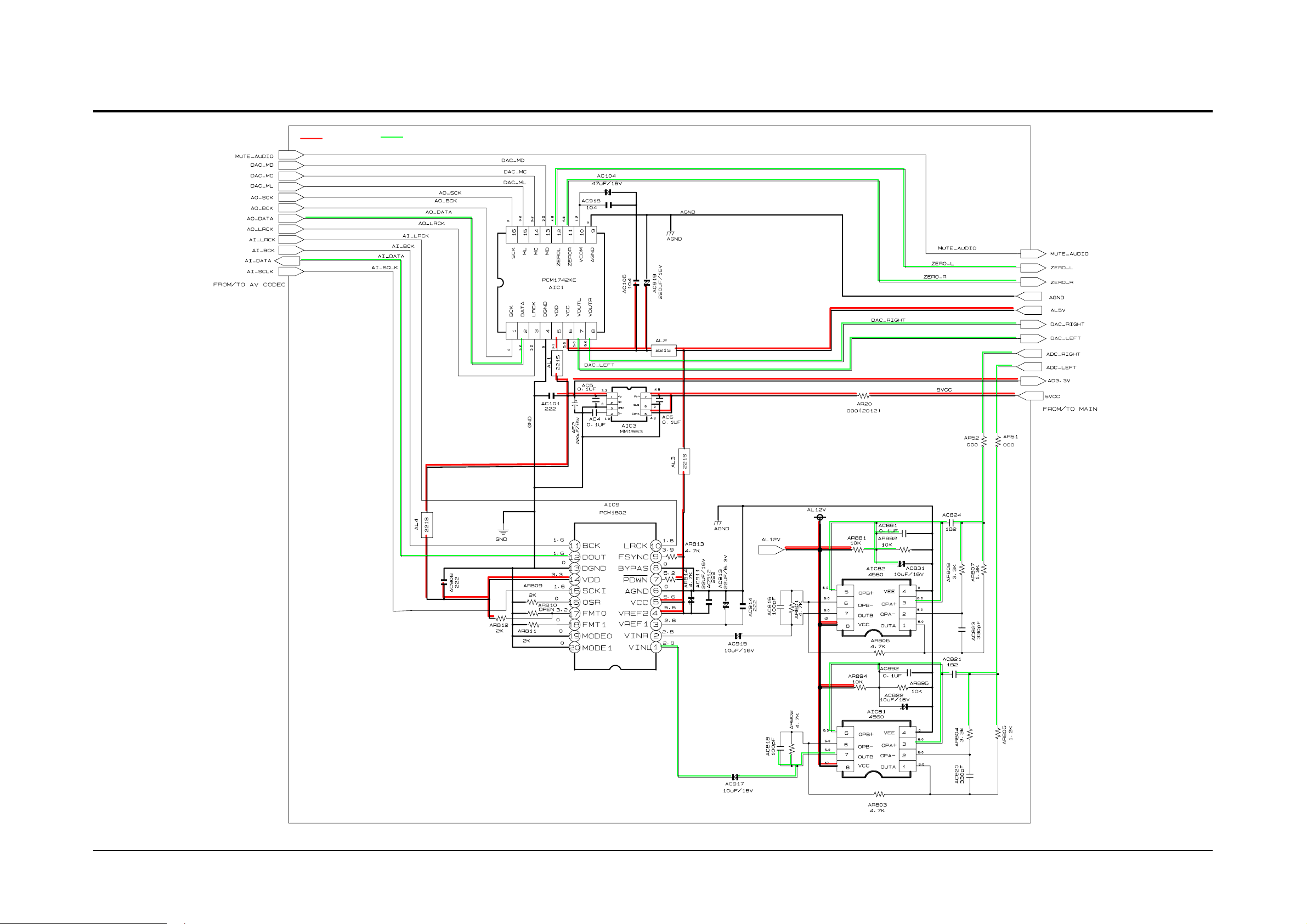
Schematic Diagrams
11-6
11-5 A/V Codec (DVD PCB)
Power
Audio
Page 9
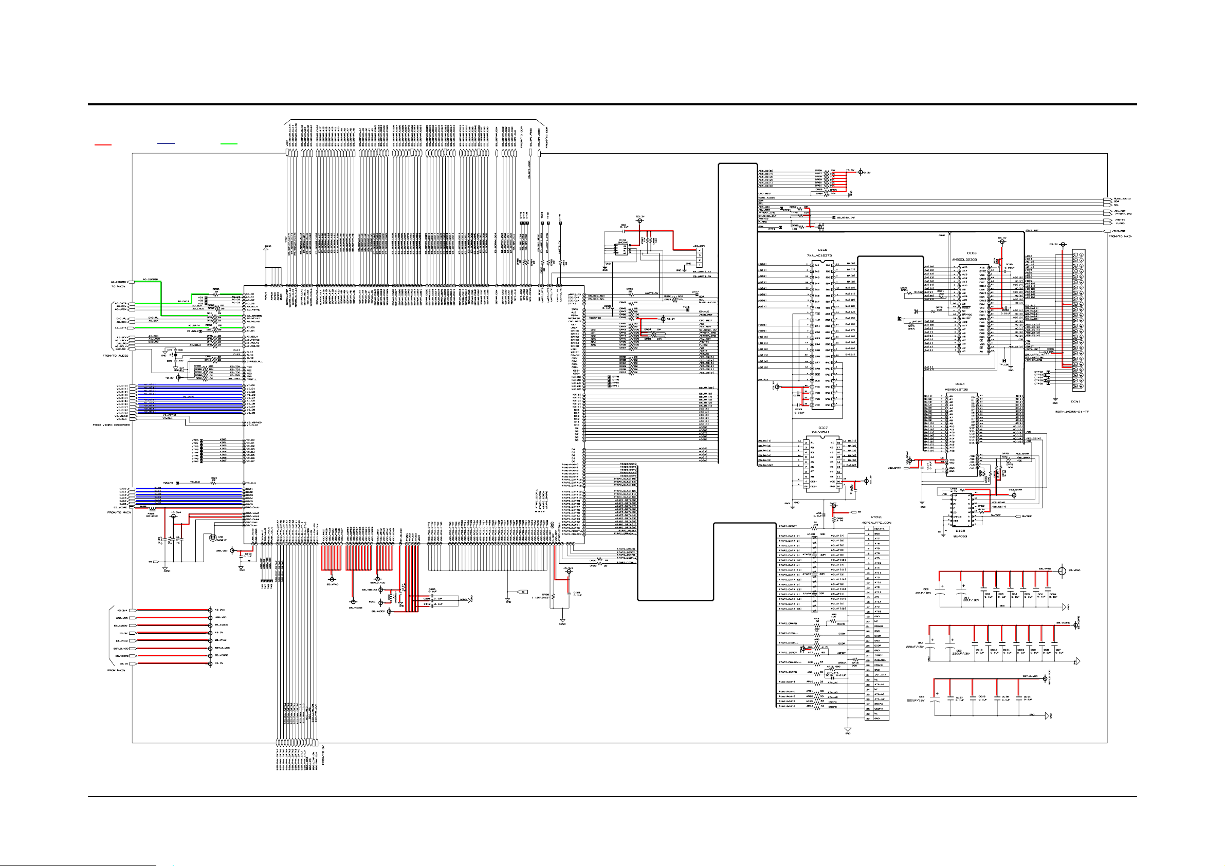
Schematic Diagrams
11-7
11-6 Audio In/Out (DVD PCB)
Power
Video
Audio
Page 10
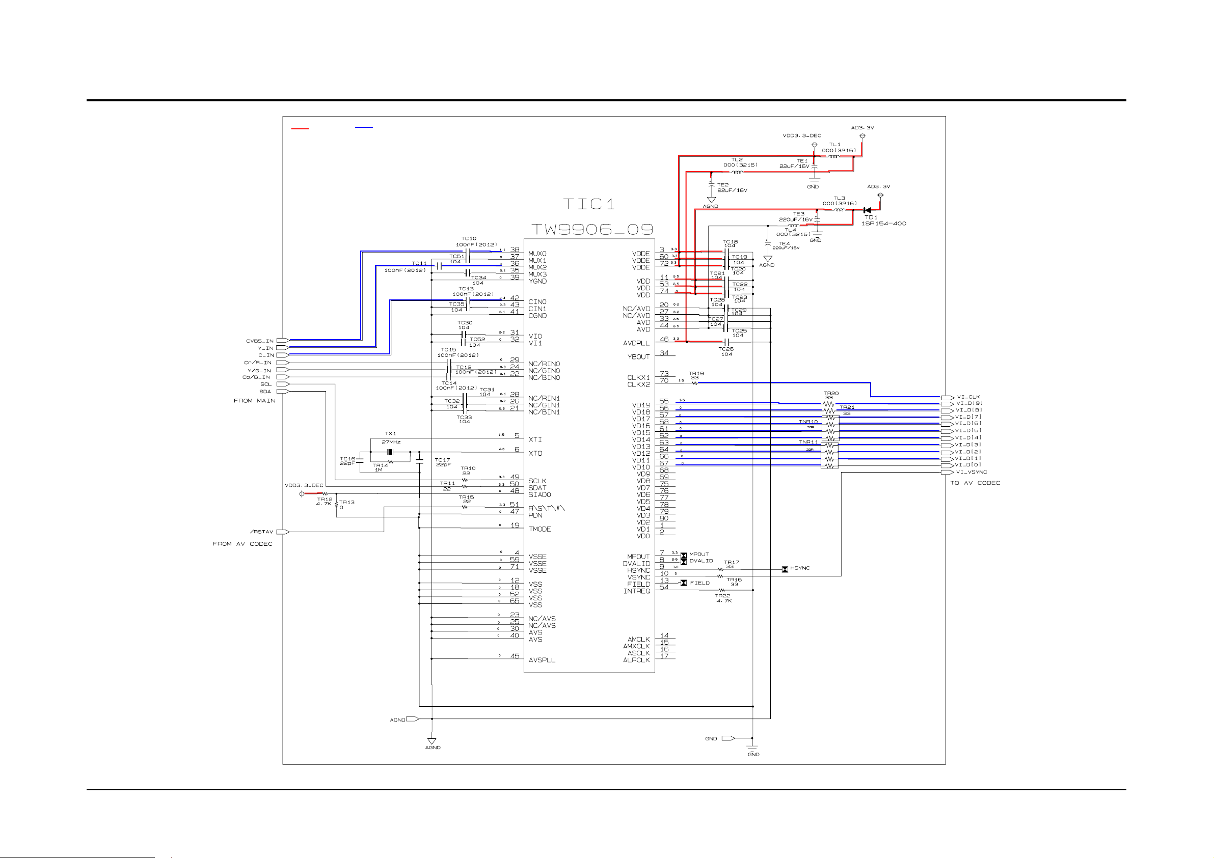
Schematic Diagrams
11-8
11-7 Video Decoder (DVD PCB)
Power
Video
Page 11
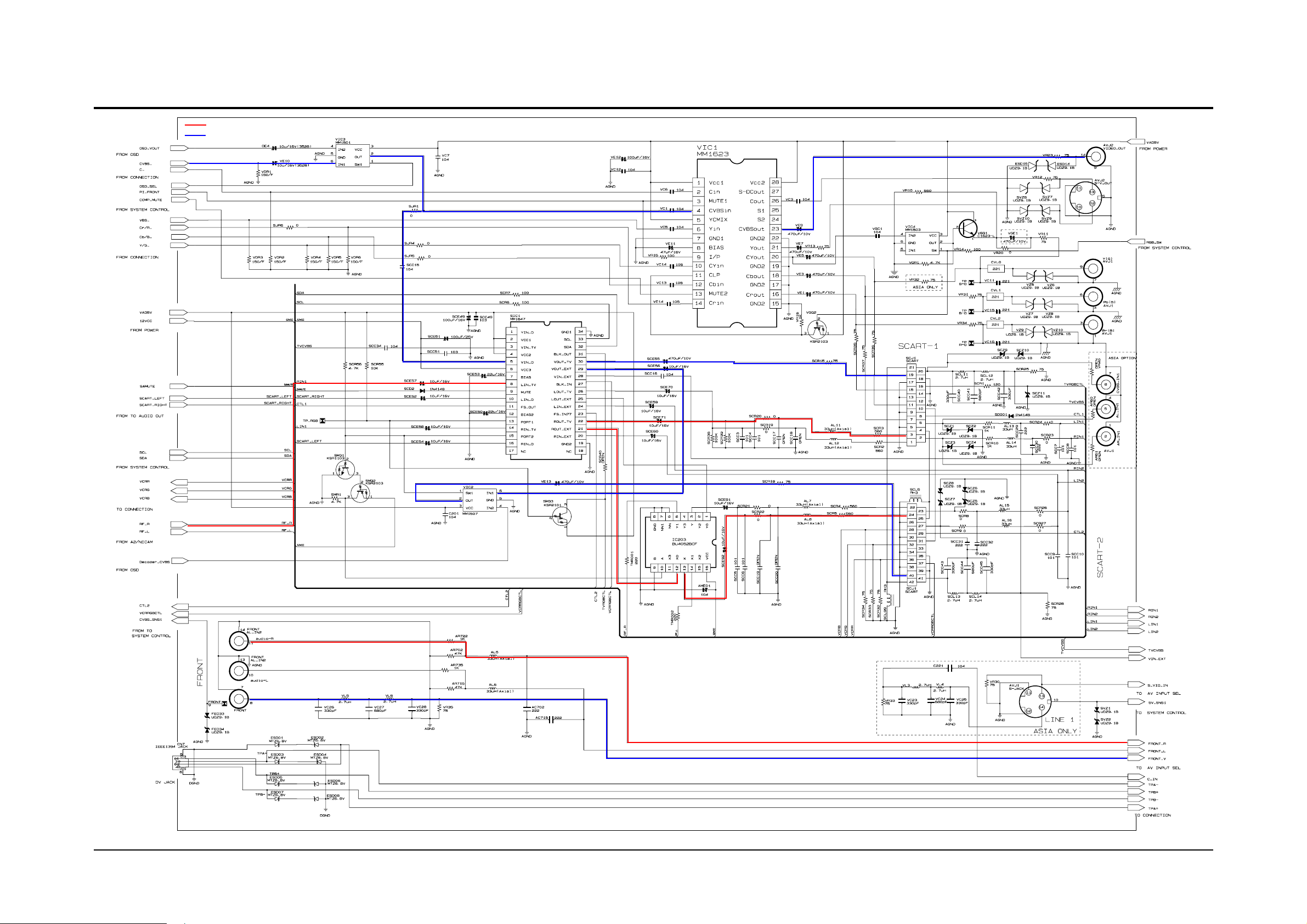
Schematic Diagrams
11-9
11-8 I/O (Jack PCB)
AUDIO
VIDEO
Page 12

Schematic Diagrams
11-10
11-9 OSD (Jack PCB)
Page 13

Schematic Diagrams
11-11
11-10 System Control (Jack PCB)
Page 14

Schematic Diagrams
11-12
11-11 TM (Jack PCB)
AUDIO
VIDEO
Page 15

Schematic Diagrams
11-13
11-12 A2/NICAM (Jack PCB)
AUDIO
Page 16

Schematic Diagrams
11-14
11-13 Power (Jack PCB)
Page 17

Schematic Diagrams
11-15
11-14 Audio Out (Jack PCB)
AUDIO
Page 18

Schematic Diagrams
11-16
11-15 Jack Connector (Jack PCB)
AUDIO
VIDEO
Page 19

Schematic Diagrams
11-17
11-16 AV Input Sellection (Jack PCB)
AUDIO
VIDEO
Page 20

13-1
13. Circuit Operating Descriptions
13-1 Power
13-1-1 About S.M.P.S (ringing choke converter methol)
◆Terms
1) 1st : Common power input to 1st winding.
2) 2nd : Circuit followings output winding of transformer.
3) f (Frequency) : Switching frequency (T : Switching cycle)
4) Duty : (Ton/T) x 100
Fig. 13-1
13-1-2 Circuit description [FLY-Back RCC(Ringing Choke Converter)] Control
(a) AC Power Rectification/Smoothing Terminal
1) PADT1 : Convert AC power to DC (Wave rectification).
2) PRCU1 : Smooth the voltage converted to DC.
3) PALT1, PALT2, PACT1, PACT2 : Noise removal at power input/output.
4) PLRU1 : Rush current limit resistance at the moment of power cord insertion.
· Without PLRU1, the bridge diode might be damaged as the rush current increases.
(b) SNUBBER Circuit : PSRZ1, PSRZ2, PSCX1, PSCZ2, PSDZ1
Transformer
(Np)
+
(Vp)
–
(Ns)
+
(Vs)
–
Vout
REGULATOR
+
Vreg
+
Vin
ON/OFF Control
Switch
+
Vs switch
–
I switch
Page 21

Circuit Operating Descriptions
13-2
Fig. 13-2
1) Prevent residual high voltage at the terminals of
switch during switch off/Suppress noise.
High inverted power occurs at switch off,
because of the 1st winding of transformer :
(V=-L1 xdi/dt. L1 : Leakage Induction)
A very high residual voltage exist on both terminals
of PQQX1 because dt is a very short.
2) SNUBBER circuit protects PQQX1 from damage
through leakage voltage suppression by RC,
(Charges the leakage voltage to PSDZ1 and PSCX1
and discharges to PSRZ1, PSRZ2).
3) PPCF2 : For noise removal
(c) PQIZ1 Vcc circuit
1) PVRL1, PVRL2, PVRL3 : PQIZ1 driving resistance (PQIZ1 works through driving resistance at power cord in)
2) PQIZ1 Vcc : PVRL4, PVDL1, PVCL1
! Use the output of transformer as Vcc,because the current starts to flow into transformer while PQIZ1 is
active
@ Rectify to PVDL1 and smooth to PVCL1.
# Use the output of transformer as PQIZ1 Vcc : The loads are different before and after PQIZ1 driving.
(Vcc of PQIZ1 decreases below OFF voltage , using only the resistance dut to lode increase after PQIZ1
driving.)
(d) Feedback Control Circuit
Fig. 13-3
Vswitch
Inverted power
by leakage
inductance
dt
0
Toff
t
PPDD2
3.3V
3
Page 22

Circuit Operating Descriptions
13-3
1) F/B terminal of PQIZ1 determines output duty cycle.
2) C-E (Collector-Emitter) of PQIZ1 and F/B potential of PQIZ1 are same.
13-1-3 Internal Block Diagram (Internal Block Diagram of S.M.P.S. Circuit)
Fig. 13-4
3.3V Rectified
Smoothing
Circuit
Rectified Circuit
Line Filter
Noise
Removal
(SNUBBER)
PWM Control
Circuit
(ICE2BSO1)
Converter
Voltage
Detection
Circuit
Smoothing Circuit
5V Rectified
Smoothing Circuit
12V Rectified
Smoothing Circuit
3.3V Rectified
Smoothing Circuit
5V Rectified
VoltageCircuit (x3)
12V Rectified
VoltageCircuit
(X3)
O
U
T
P
U
T
Power IN
(110V)
Page 23

Circuit Operating Descriptions
13-4
13-2 AV Codec
Fig. 13-5
· Main system control · ATAPI interface with DVD-Multi Drive
· A/V Encoding/Decoding · Analog Progressive/interlaced video output
· Transcoding/rating
· IEEE 1394 link layer function
DVD
MULTI DRIVE
(SERVO)
IEEE 1934
(DV input) block
Audio input
block
U23,U24
M13S128168A
(DDR SDRAM)
DIC3
AM29DL323GB
(Flash Memory)
PIC1
TSB41AB1
(1394 PHY)
AIC9
PCM1802
(AUDIO A/D)
32bit
16bit
8bit
I2S
SDRAM I/F
HOST I/F
DV I/F
AUDIO IN
ATAPI
DIC1
DMN8602
(A/V CODEC)
AUDIO OUT
(Digital,Ainalog)
VIDEO OUT
IEL-P58
Audio output block
I2S
Y,Pb,Pr, Y/C, CVBS
LOAXIAL
OPTILAL
AIC1
PCM1742KE
(AUDIO D/A)
Video output
block
Video input
block
TIC1
TW9906
(VIDEO DEC)
ITU-R656
VIDEO IN
Front Panel I/F
IC601
MN101DF10G
(Front MICOM)
Page 24

Circuit Operating Descriptions
13-5
13-2-1 DIC1 Processor Internal Architecture Diagram
Fig. 13-6
13-2-2 A/V Processor (DIC1) Functional description
1) SPARC Processors
Two 32-bit SPARC processors, one dedicated to video processing and the other assigned general system tasks
and audio processing, perform three classes of functions: system processing, audio processing, and high-level
control flow and decision-making tasks for video processing. Optionally, they can also perform 2D graphics
and host functions.
The DMN8602 also support multiple video inputs, windowed video ad graphics with arbitrarily relocatable
and resizable windows, letterbox, and side-by-side display of SD sources.
2) Host Interface
The host communication functions include initialising the DMN-8602 device, downloading software to the
local SDRAM, sending commands, monitoring status, and downloading graphics data such as OSD bitmap.
2Port
4Port
1X10 YUV
Audio
Interface
SPARC Processor Core
Data
I - Cache Memory/
Cache
Audio DSP Host
And And
Memory Graphics
Video
Interface
Host
Interface
SPDIF
Video DSP
and memory
16/32
64
Bitstream/
Storage
Inter face
SPARC Processor Core
Data
I - Cache Memory/
Cache
Audio DSP Host
And And
Memory Graphics
Motion
Estimator
and memory
1394
Link
Interface
Memory/
Cpntroller
Serial I/O
SDRAM
32
DENC
Page 25

Circuit Operating Descriptions
13-6
3) Bitstream/Storage interface
◆ ATAPI Controller
ATAPI is an asynchronous, 120ns, 16-bit word interface commonly used to connect devices such as hard
disks, CD/DVD ROMs, and DVD RAMs. All operations are initiated by reading/writing a set of ATAPI
device registers through programmed input/output(PIO) data transfer. ATAPI has DMA commands for
transferring long data. The ATAPI register address is defined by the output pins CS0, CS1, DA[2:0].
◆ The IEEE1394 interface can receive MPEG-2 transport stream or DV stream data contained in isochronous
packets (IPs). The DMN-8602 device filters the packets by matching channel IDs. In the case of MPEG-2
transport streams, the DMN-8602 device performs descrambling on the data that is scrambled with 5C
encryption. Software is responsible for transport section processing and demultiplexing.
4) Video Interface
◆ Video Input channel
The video input channel captures ITU-R BT.656-compliant 10-bit digital YUV component video stream from
Video decoder chip(TIC1)
◆ Video Digital Encoder (DENC)
The NTSC/PAL digital video encoder (DENC) module converts a digital video data stream into NTSC or
PAL composite or component video output.
The DMN-8602 DENC output can be in one of the following formats:
•Baseband composite NTSC (M) or PAL (B,D,G,H,I) analog video.
•Separate analog luma(Y) and chroma(C) output to support S-Video.
•Separate analog component video RGB or SMPTE YPbPr output.
5) Audio Interface
The serial audio input port receives uncompressed 16- to 24-bit serial digital audio data from external audio
ADC(AIC9). An internally generated clock provides bit serial clocking of the data coming from external ADC
The serial audio output port sends uncompressed 16- to 24-bit serial digital audio data to external audio
DAC(AIC1). An internally generated clock provides bit serial clocking of the data coming from external ADC
6) Serial I/O interface
◆ SPI interface
The SPI(Serial Peripheral Interface) port provides a bus for a serial interface with front panel micom(FIC1)
◆ IDC interface
The IDC bus is a simple, two-wire, bidirectional communication bus. The two signals, clock and data, are com
mon to every device connected to the bus.
In this system, IDC bus is connected to EEPROM(DIC8) and Video Decoder(TIC1)
Page 26

Circuit Operating Descriptions
13-7
13-3 SERVO (DVP Multi Drive)
1) Pick-Up
Data in the disc is processed from the optical pick-up unit (OPU). OPU includes the Elantec chip (EL6912c)
which is a highly integrated laser diode driver designed to support multi-standard writable optical drives. This
chip also has an IV amplifier with concurrent read and write sampling. The architecture allows reprogramming
of the timers to support different media DVD or CD standards, and different speed.
2) A-Chip
A chip is RF processor. This module performs RF signal processing which includes RFIP, RFIN, AGC, RF equal
izer. This processor is able to detect tracking error, focus error and various signals such as CE, PE, SBAD,
DEFECT, BCA, MIRROR, Wobble, TZC, RC, and RECD.
3) C-Chip
C-Chip is composed of DP1, PRML and WS.
First, the Data processor1 (DP1) performs EFM/EFM+ Demodulation and data is stored in the buffer
memory in data processor2 (DP2). DVD data in this buffer is transferred to CSS/ATAPI through
error-correction code
(ECC), descramble process and error detection code (EDC).
Second, WS performs the following processes.
! Delay compensation using Shift register
@ Sample/Hold pulse generation
# I/V Gain Control
$ Providing clock for RF chip
% OPC Control signal generation
Lastly, PRML completes the adaptive EQ/VD and Digital PLL.
4) D-Chip
D-Chip consists of Servo DSP, DP2 and 1Mbit memory. Servo DSP is dealing with controlling the servo-mecha
nism in DVD recorder. Servo-DSP has the following features.
! Bulit-in 10Bit ADC(8ch), DAC(3ch) and PWM(7ch)
@ Step Motor Control Logic: Macro/Micro Step
# Track Counter: long distance velocity control direct seek
$ Shock/Defect detection
% Header (DVD-RAM)/Land Pre-Pit (DVD-R/RW) Detection
^ Several Servo Monitor Signal Detection
& RF IC Interface
* Micom Interface
( Digital Servo Control of focus, tracking, sled and seek
) Disc Auto-Detection
1 Automatic Adjustment of the offset, balance and gain of Focus and Tracking Signal
2 Direct Seek with Velocity Control
3 Step Motor Control: Macro Seek
4 De-Track and Lens Shift Detection and Compensation
5 Center Error Control
6 DVD Layer Jump
7 Tilt Detect and Compensation
DP2 performs High Speed ECC and CD DA Decoder.
Page 27

Circuit Operating Descriptions
13-8
5) ATAPI Controller
ATAPI (ATA Packet Interface) the standard interface protocol used to connect the CD/DVD Drive to IDE inter
face. Data from the front-end is processed to back-end through this ATAPI protocol. Sanyo chip (LC98600CTXB0) is utilized for ATAPI interface. LC98600CT-XB0 has the following features.
! ECC and EDC correction/addition for CD-ROM data
@ Subcode decoding/encoding
# Spindle servo control
$ CLV/CAV servo control using ATIP data
% ATIP decoding and CRC check functions
^ Providing random EFM output for PCA use
& High-accuracy write strategy signal output enabled (CD-R 52x)
* Buffer RAM can be accessed by the microcontroller through the LC98600CT-XB0
( Built-in ATA-PI(IDE) interface (supports Ultra DMA modes 0,1, and 2)
) 52x decoding speed/52x encoding speed supported with 33.8688Mhz
1 Maximum transfer speed PIO mode: 16.6 MB/s (with IORDY), Ultra-DMA: 66MB/s (with DMARQ)
2 User can freely set the CD main channel, C2 flag, and subcode areas in buffer RAM
3 Built-in batch transfer function for transferring (CD main channel, C2 flag, etc., in a single operation)
4 Built-in multi-transfer function (allows multiple blocks to be sent to the host automatically in a single
operation)
Fig. 13-7
Pick up
Deck
Sled
Motor
FPD,PD,I/V amp
LD,LD Driver
Focus Actuator
Tracking Actuator
TILT Actuator
Spindle
Motor
Tray
Motor
A.chip (RIC1)
RF Signal
(AGC/EQ)
Servo Error
(FE/TE/CE/PE
SBAD/RC/TILT)
Miscellaneous
Signal
(DFT/LPP
/WOBBLE)
APC & OPC
Motor
Driver
C.chip (CIC1)
PRML
ENDEC
WRITE
STRATEGY
D.chip (DIC1)
SERVO
Processor
ECC
Processor
MICOM (MIC1)
HOST
ATAPI chip
(ZIC1)
Page 28

Circuit Operating Descriptions
13-9
13-4 Video In/out Block
This Model has the two single CVBS Video input(AV3) and two Scart input from AV1 or AV2.
AV3 Video input is CVBS at the at the Front Panel. AV2 Scart has CVBS & RGB input and CVBS output, AV1
Scart is vice versa at the Rear Panel.
The analog Video signal is selected by the IC201(BU4051 Mux). It is controlled by FIC1 (Front Micom).
TIC1 (Video Decoder) diverges from the 14.318185MHz crystal, then generates ITU-R656 (10bits) and 27MHz
clock.
TIC1 (Video Decoder) does closed caption, copy guard detect processing and A/D conversion of analog Video
signal converted into 11bit Digital Video signal (ITU-R656 Format) is outputted via DIC1 (MPEG2 Decoder &
Encoder with video Encoder) of digital part.
13-4-1 Outline
DIC1 (MPEG2 Decoder & Encoder with video Encoder) diverges from the 13.5MHz crystal, then generates
VSYNC and HSYNC.
DIC1 (MPEG2 Decoder & Encoder with video Encoder) does RGB encoding, copy guard processing and
D/Aconversion of 10bit Video signal converted into analog signal is outputted via amplifer of analog part.
DIC1 inputted from pin E1 with 13.5MHz generates HSYNC and VSYNC which are based on video signal. DIC1
is synchronous signals with decoded video signal.
The above signals, which are CVBS (Composite Video Burst Synchronized), Y(S_Video),
C(S_Video),Y(Component)/G(Green), Cr(component)/R(Red), Cb(component)/B(Blue), are selectively outputted
576i(interlaced Video Output), 576P(progressive Video Output).
DIC1 adopts 10bit D/A converter. DIC1 perform video en-coding as well as copy protection.
Fig. 13-8
OSD_SEL
MPEG-2
A/V CODEC
(DIC1)
Video
Decoder
(TIC1)
RGB
CVBS/Y
74HC4051
(IC201)
OSD
CVBS
RF
AV3
AV1 (CVBS)
AV2 (CVBS)
MM1647
(SIC1)
Front Micom
CVBS
RF Tuner
MM1501
(VIC3)
NJM 2267
(6dB AMP)
MM1623
(VIC1)
MM1507
(VIC2)
POST2
VPS/Sync
Detector
S-Video 1
Video 1
Component
RGB
Y/C
CVBS
SCART1 (TV)
SCART2 (EXT)
OSD
Page 29

Circuit Operating Descriptions
13-10
13-4-2 Video Switch (MM1507:VIC2,MM1501:VIC3)
MM1501, 1507 is 2 by 1 Video switch and VIC2 is switched by Pin15 of SIC1. It selects from RF Video signal via
TIC2(NJM2267) for Decoder CH. or normal video output via SIC1.
VIC3 is switched by Pin23 of FIC1. It selects Video Output from DIC1 or OSD SCREEN for Optional setting.
13-4-3 Analog Mux (BU4051, MM1501)
IC201(BU4051) and IC202(MM1501) are Analog Mux.
As input selecttion Pin(9, 10, 11) of the IC201 are controlled by the Front Micom, IC201 select among AV1 CVBS,
AV2 CVBS, AV3 CVBS, RF CVBS signal.
13-4-4 MUX IC for 2SCART (MM1647)
SIC1(MM1647) is Audio & Video switcher with I2C bus for Two SCART. I2C bus is connected with FIC1(Front
micom) and be control Pin 30 for AV1 CVBS OUTPUT is selected from pin 5, pin 28.
Pin 29 for AV2 CVBS OUTPUT is selected from pin 5, pin 3.
Fig. 13-9
YIN D
GND1
12V
5V
VCC1
SCL
I2C LOGIC
VIN TV
VCC1
5V
YIN D
VCC2
BIAS
LIN TV
MUTE
LIN D
FS OUT
BIAS2
PORT1
RIN TV
SDA
BLK OUT
VOUT TV
VOUT EXT
VIN EXT
BLK IN
LOUT TV
LOUT TV
LIN EXT
FS IN
ROUT TV
ROUT EXT
PORT2
RIN D
NC
RIN EXT
GND 2
NC
Page 30

Circuit Operating Descriptions
13-11
13-4-5 NTSC/PAL Video Decoder (TW9909 : Video Decoder)
The TIC1 (Video Decoder : TW9909) device is a high quality, single-chip digital video decoder that digitises and
decodes all popular baseband analog video formats into digital component video. The TIC1 (Video Decoder
:TW9909) supports the analog-to-digital (A/D) conversion of component RGB and YPbPr signals, as well as the
A/D conversion and decoding of NTSC, PAL and SECAM composite and S-video into component YCbCr.
This TIC1 (Video Decoder : TW9909) includes four 10-bit 30-MSPS A/D converters. and A/D conversion of 10bit
analog Video signal converted into Digital Video signal (ITU-R656 Format) is outputted via DIC1 (MPEG2
Decoder & Encoder with video Encoder) of digital part.
The following output formats supply 10-bit 4:2:2 YCbCr to the DIC1 (MPEG2 Decoder & Encoder with video
Encoder) of digital part.
On CVBS and S-video inputs, the user can control video characteristics such as contrast, Brightness, saturation,
and hue via an I2C DIC1 port [PIN V17, V18] interface.
The TW9909 decoder includes methods for advanced vertical blanking interval (VBI) data retrieval. The VBI data
processor (VDP) slices, parses, and performs error checking on teletext, closed caption (CC), Copy Guard Detect
Processing and other VBI data.
13-4-6 Amplifier (MM1623)
VIC1 is 6dB amplifier.
Based on CVBS signal, the final output level must be 2Vpp without 75ohm terminal resistance.
Because the level of video encoder output is only 1Vpp, the level is adjusted with the special amplifier.
When mute of pin 3 is high active, if the pin is floating and connect to power, the output signal is never outputted.
CVBS, Y, C, Y(R), Cb(B), Cr(R) outputted from video encoder are inputted to VIC1 [Pin4, 6, 2, 10, 12, 14] respectively.
The signal to which gain is adjusted by amplifier is outputted from jack via 75ohm Resistance
(VR14, 15, 16, 23, 12, 13).
Page 31

Circuit Operating Descriptions
13-12
13-5 Audio
Fig. 13-10
13-5-1 Audio Input Block
This Model has tree stereo line input terminals and internal TV-audio from RF Tuner Block.
These four analog audio signal source are converted to digital data by Input Block.
Input Block has Multiplexer(AIC51), Input Filter(AIC81, AIC82), and A/D Converter(AIC9).
The switching operation of AIC51 is controlled by FIC1(Front Micom) with I2C interface.
The signal selected by AIC51 are filtered by AIC81,AIC82.
The funtion of these OP-Amp is -6dB level scaling and second order Low Pass Filtering.
AIC9 is syncronized by three Digital clock from DIC1,
and output Digital signal to DIC1(Dolby Digital Encoder/Decoder).
AV1 In
(SCART 1)
AV2 In
(SCART 2)
AIC81
AV3 IN
(Rear)
AV4 IN
(Front)
TV Audio
(from tuner
block)
AIC51
BD3824FS
Audio
Multiplexer
4560 OP-AMP
AIC82
4560 OP-AMP
AIC9
PCM1802
(Audio A/D
Converter)
DIC1
DMN8602
A/V Processor
(Dolby Digital
Encoder/Decoder)
FIC1
Front Micom
IIC
Switch Control
Page 32

Circuit Operating Descriptions
13-13
13-5-2 Audio output Block
This Model has four stereo analog line out terminal, and two digital output terminal.
Decoded signal by DIC1 is inputted to AIC1( D/A converter), then filtered and amplified by AIC4(OP-amp), and
finally ouputted via RCA terminal and Scart terminal.
The Signal outputted via AV2 is equal to those of AV1(Scart), and RCA Analog ouput terminal in normal mode.
The Digital audio signal is drived by AIC3 inverter and ouputted via Optical(TOS-link) and Coaxial(S/PDIF)
terminal.
Fig. 13-11
AV1
(TV)
SICI
MM1647
Scart IC
AIC5
4560
Buffer
Control
Signal
IC203
Audio
Multiplexer
SCART
Audio Out
AV2
(EXT)
AUALOG
AUDIO OUT
(RCA terminal)
Optal
Out
Coaxial
Out
Tuner Block
L1
R1
L2
R2
AIC4
4560 OP-AMP
AIC3
74HCU04
(Inverter for Digital Out)
L-OUT
R-OUT
AIC1
PCM1742KE
(Audio D/A
Converter)
DIGITAL Audio DATA
SCKI
BCK
LRCK
DOUT
ML
MC
MD
DICI
DMN8602
A/V Processor
(Dolby Digital Encoder/Decpder)
Page 33

Circuit Operating Descriptions
13-14
13-6 Tuner
1) Low Pass Filter & High Pass Filter
This consists of IF trap circuit and UHF & VHF separation circuit. If the input signal is IF (45.75MHz),
this filter
prevents interference.
2) Single tune
This consists of a filter circuit, RF AMF, impedance conversion circuit, image trap and a single tuning circuit. It
prevents noise and other interference signals. It is very important part which improves NF (noise figure) and
prevents the various of spurious signals.
3) RF AMF
RF AMF is made of FET (Field Effects Transistor). It is controlled by AGC coming from IF DEMOD block.
4) Double tune
It consists of a double tuning circuit to improve characteristic of rejection that results in a better band
characteristic.
5) Mixer IC (Mixer, OSC, PLL)
It consists a VHF and UHF OSC and Mixer circuit. We applied mixer to make better characteristic of rejection,
it shows especially various beat characteristic.
6) PLL IC
The PLL IC plays a role selection of Tuner channel. It was built-in three wire PLL IC, charge pump and band
driver.
The minimum of step frequency is 31.25KH z.
Fig.13-12
Fram IF Sectlon
>
<
10
14
<
<>
L
V
V
9
8
Band Driver
3wice Bas
Recelver
13 12
AGC
TO IF Sect lon
>
IF
Fram IF Sect lon
+B
H
U
6
4MHz
15 X-tal
Fran
Modulafor
a
VHF
8.P.F
~
~
~
VHF
Single Tune
VHF
b
SingleTune
VHF
-RF Amp
VHF
c
RF Amp
VHF
Double Tune
VHF
d
Double Tune
VHF Mixer
e
35
1
Mixer
OSC 8uffer
Mix IC IC100
VHF
VHF OSC
IF Amp
VHF OSC
78
VHF OCS
12
9
OSC Amp
L.P.F
IF Single
f
PLL IC
4
1/8 Prescaler Band Driver
Prog.Dirlder
3
2
Phese Code
1
Charge Pump
16
~
1
^
&
PB
TU
*(
CLOCK DATA ENABLE
LOCK
1
)
Page 34

Circuit Operating Descriptions
13-15
13-7 IF
1) SAW FILTER
It passes only needed band of the signal that is converted to IF frequency and decrease the others band to
minimize the effect of adjacent channel.
2) RF AGC Control
It used adjusting to determine RF AGC working point in tuner.
3) VCO Tank
When VCO tank detects PLL, it makes the signal which sets a standard.
4) AFT (Auto Frequency Tuning)
AFT automatically controls the oscillator frequency in the tuner, so that it retains a constant level.
It is a quadrature detection type. The carrier, which is detected from video det is directly input to AFT.
The 90 degree delayed phase signal is input at the same time to AFT and, the results come out.
5) IF AMP
IF signal , which is selected in Saw filter, is amplified in IF amp frequency enough to be detected. The IF amp
has parallel inputs & outputs structure.
Fig. 13-13
From
Tuner Section
To Tuner Section
RF AGC
To Tuner Section
b
RF AGC Control
(IF Amp)
d
4.5 MHz
Tunlng
a
SAM Filter
AFT Tank
1
2
4
5
6
10
11
12
RF AGC Amp
AFT
FM Det
Pra
Amp
Video Det
APC
Det
Video Amp
N.S.C
APC Tine
Const SW
Mix
Lock Det
IF AGC
Lim Amp
AGC
EQ.Amp
B/W
VCD
24
21
19
17
16
15
14
3
4
+B
AUDIO OUT
SIF filter
4.5MHz
SIF Trap
c
VCD Tank
56
AFT OUT VIDEO OUT
 Loading...