www.ti.com
FEATURES APPLICATIONS
DESCRIPTION
Curre nt
Limit Logic
ILIM
CLF
AGND
3V3
3V3
REG
Driv e andDe ad-Time
Contr olLogic
(D;1-D)
UVLO
I
DLY
+
CS
BIAS
CS+ BST OUT1 SW PVDD OUT2 PGND
Enable
IO
+
0.6 V
POS
NEG
+
AO
VDD
+
ILIM/10
48x
Over
Curre nt
IN
SRE
Blank
UCD7230
DLY
I
LOAD
PWM
SRE
V
OUT
I
DLY
V
IN
BIAS
I
MAX
CLF
UCD7230
SLUS741C – NOVEMBER 2006 – REVISED MARCH 2007
Digital Control Compatible Synchronous Buck Gate Drivers with Current Sense
Conditioning Amplifier
• Digitally-Controlled Synchronous-Buck Power
• Input from Digital Controller Sets Operating
Stages for Single and Multi-Phase
Frequency and Duty Cycle
Applications
• Up to 2-MHz Switching Frequency
• Especially Suited for Use with UCD91xx or
• Dual Current Limit Protection with
UCD95xx Contollers
Independently Adjustable Thresholds
• High-Current Multi-Phase VRM/EVRD
• Fast Current Sense Circuit with Adjustable
Regulators for Desktop, Server, Telecom and
Blanking Interval Prevents Catastrophic
Notebook Processors
Current Levels
• Digitally-Controlled Synchronous-Buck Power
Supplies Using µ Cs or the TMS320TM DSP
• Digital Output Current Limit Flag
Family
• Low Offset, Gain of 48, Differential Current
Sense Amplifier
• 3.3-V, 10-mA Internal Regulator
The UCD7230 is part of the UCD7K family of digital
• Dual TrueDrive™ High-Current Drivers
control compatible drivers for applications utilizing
• 10-ns Typical Rise/Fall Times with 2.2-nF
digital control techniques or applications requiring
Loads
fast local peak current limit protection.
• 4.5-V to 15.5-V Supply Voltage Range
Please be aware that an important notice concerning availability, standard warranty, and use in critical applications of Texas
Instruments semiconductor products and disclaimers thereto appears at the end of this data sheet.
TrueDrive, PowerPAD are trademarks of Texas Instruments.
PRODUCTION DATA information is current as of publication date.
Copyright © 2006–2007, Texas Instruments Incorporated
Products conform to specifications per the terms of the Texas
Instruments standard warranty. Production processing does not
necessarily include testing of all parameters.
www.ti.com
SIMPLIFIED APPLICATION DIAGRAMS
DLY
SRE
AGND
3V3
UCD7230
IN
VDD
DPWMB0
UCD9112
A0
I0
CLF
ILIM
DPWMA0
RB1/TMRI1
OUT1
CSBIAS
SW
6
5
4
2
COMMUNICATION
(Programming&
StatusReporting)
1
VIN
10
7
9
8
OUT2
2
1
3
2
2
ADC2
RB0
AD33
EAP
EAM
VOUT
VOUT
VD25
RST
ADC3
AVSS
2
1
RNEG
RPOS
GSENSE
GSENSE
20
18
CS+
15PVDD
19
17
BST
16
12NEG
14
PGND
13
11POS
UCD7230
SLUS741C – NOVEMBER 2006 – REVISED MARCH 2007
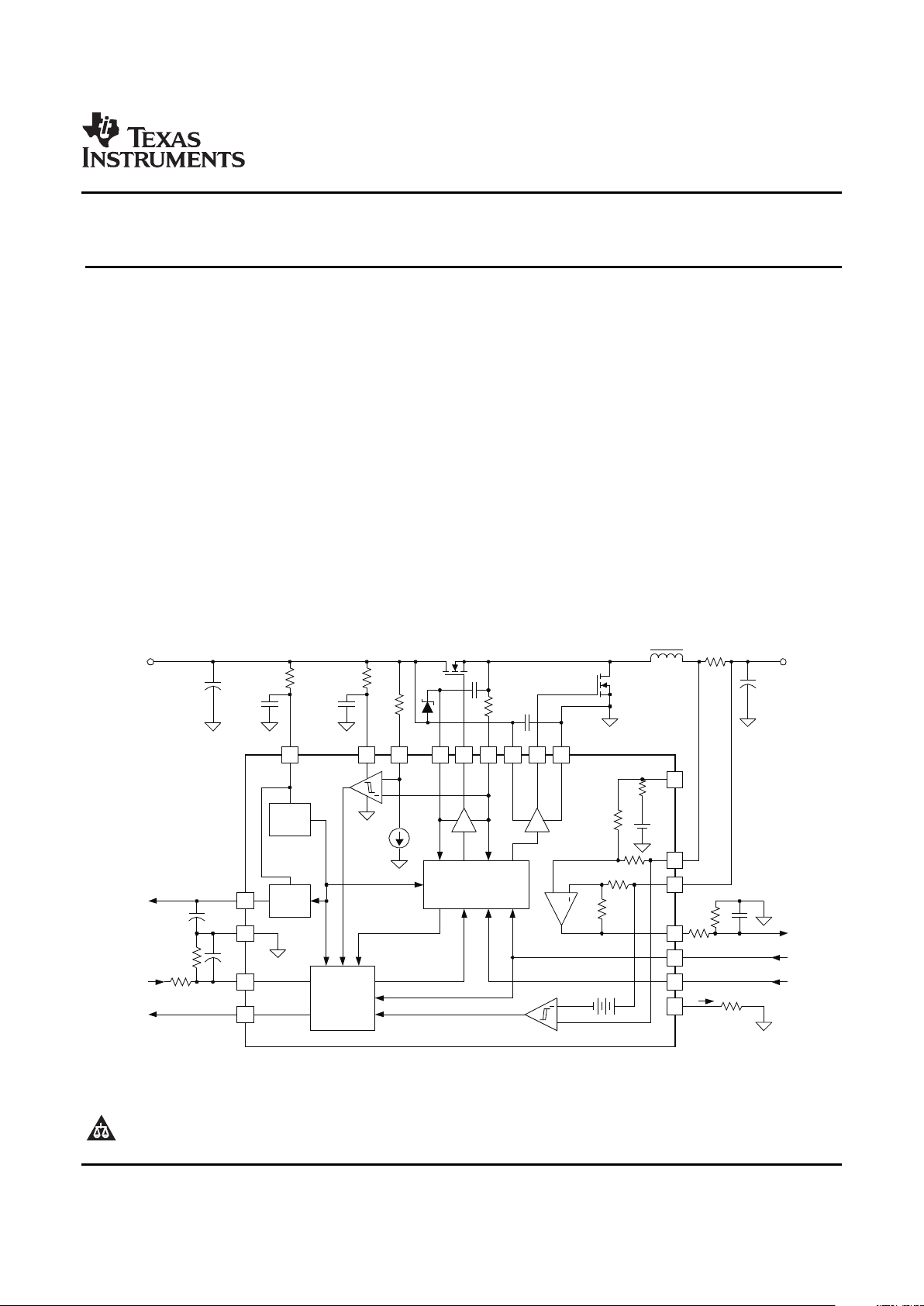
The UCD7230 is a MOSFET gate driver specifically designed for synchronous buck applications. It is ideally
suited to provide the bridge between digital controllers such as the UCD91xx or the UCD95xx and the power
stage. With cycle-by-cycle current limit protection, the UCD7230 device protects the power stage from faulty
input signals or excessive load currents.
The UCD7230 includes high-side and low-side gate drivers which utilize Texas Instrument’s TrueDrive™ output
architecture. This architecture delivers rated current into the gate capacitance of a MOSFET during the Miller
plateau region of the switching. Furthermore, the UCD7230 offers a low offset differential amplifier with a fixed
gain of 48. This amplifier greatly simplifies the task of conditioning small current sense signals inherent in high
efficiency buck converters.
The UCD7230 includes a 3.3-V, 10-mA linear regulator to provide power to digital controllers such as the
UCD91xx. The UCD7230 is compatible with standard 3.3-V I/O ports of the UCD91xx, the TMS320TM family
DSPs, µ Cs, or ASICs.
The UCD7230 is offered in PowerPAD™ HTSSOP or space-saving QFN packages. Package pin out has been
carefully designed for optimal board layout
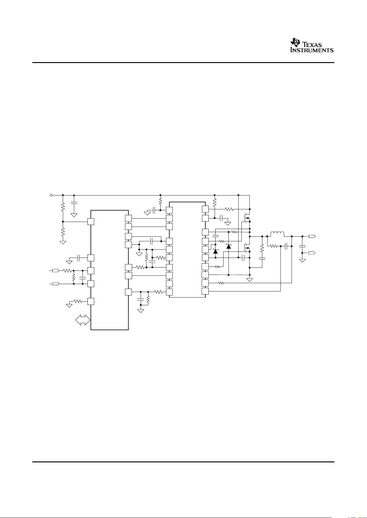
Figure 1. Single-Phase Synchronous Buck Converter using UCD9112 and one UCD7230
2
www.ti.com
20
18
CS+
OUT1
CSBIAS
SW
15PVDD
2
6
3
5
4
DLY
SRE
AGND
3V3
UCD7230PWP
COMMUNICATION
(Programming&
StatusReporting )
19
17
1
IN
BST
16
1
VDD
VIN
DPWMB0
UCD9112
10
7
9
8
A0
I0
CLF
ILIM
OUT2
12NEG
14
PGND
13
11POS
2
DPWMA0
2
2
ADC2
RB0
AD33
RB1/TMRI1
EAP
EAM
VOUT
VOUT
VD25
RST
ADC3
AVSS
20
18
CS+
OUT1
CSBIAS
SW
15PVDD
2
6
3
5
4
DLY
SRE
AGND
3V3
UCD7230PWP
19
17
1
IN
BST
16
1
VDD
10
7
9
8
A0
I0
CLF
ILIM OUT2
12NEG
14
PGND
13
11POS
2
2
2
2
ADC5
RB3/TMRI0
RB0
RB0
DPWMA1
1
DPWMB1
RPOS1
RNEG1
RPOS2
RNEG2
GSENSE
GSENSE
UCD7230
SLUS741C – NOVEMBER 2006 – REVISED MARCH 2007
SIMPLIFIED APPLICATION DIAGRAMS (continued)
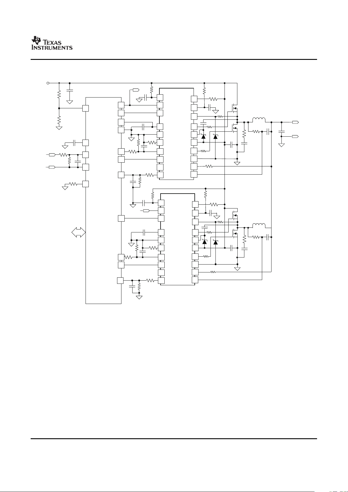
Figure 2. Multi-Phase Synchronous Buck Converter using UCD9112 and two UCD7230
3
www.ti.com
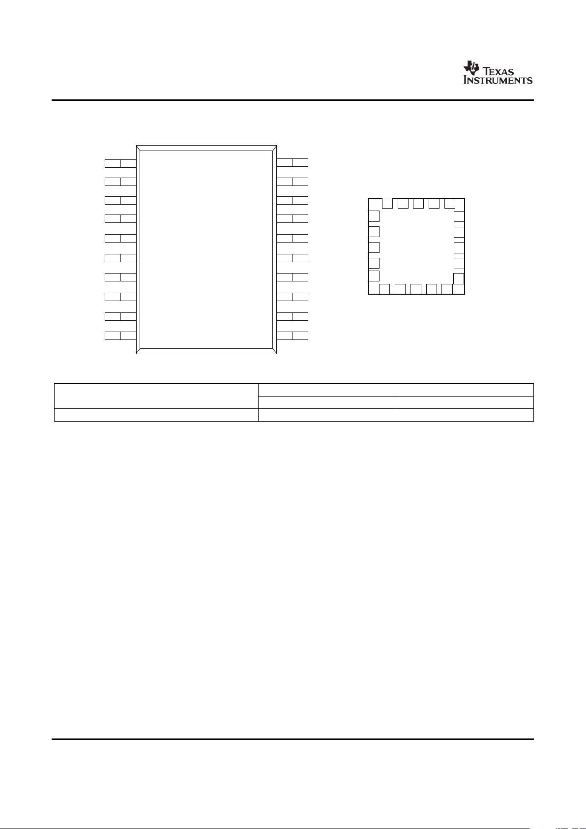
CONNECTION DIAGRAMS
UCD7230
(HTSSOP)
UCD7230
(QFN -
RGW)
(5x5, 0.65)
17
16
15
14
13
12
4
5
6
7
8
9
3V3
AGND
DLY
I0
A0
OUT1
PVDD
OUT2
1110
POS
PGND
ILIM
NEG
CLF
BST
183
IN
SW
4
2
3
10
15
14
13
12
3V3
AGND
DLY
ILIM
SRE
OUT1
BST
PVDD
19 18 17 16
1
7 8 9
CS+
CSBIAS
SW
PGND
NEG
A0
POS
VDD
11 OUT2
6
I0
5
CLF
IN
20
2
1
19
20
SRE
VDD
CSBIAS
CS+
UCD7230
SLUS741C – NOVEMBER 2006 – REVISED MARCH 2007
ORDERING INFORMATION
(1) (2)
PACKAGED DEVICES
TEMPERATURE RANGE
PowerPAD™ HTSSOP-20 (PWP) QFN-20 (RGW)
-40°C to + 125°C UCD7230PWP UCD7230RGW
(1) These products are packaged in Pb-Free and green lead finish of Pd-Ni-Au which is compatible with MSL level 1 at 255-260°C peak
reflow temperature to be compatible with either lead free or Sn/Pb soldering operations.
(2) HTSSOP-20 (PWP), and QFN-20 (RGW) packages are available taped and reeled. Add R suffix to device type (e.g. UCD7230PWPR) to
order quantities of 2,000 devices per reel for the PWP package and 1,000 devices per reel for the RGW packages.
4
www.ti.com
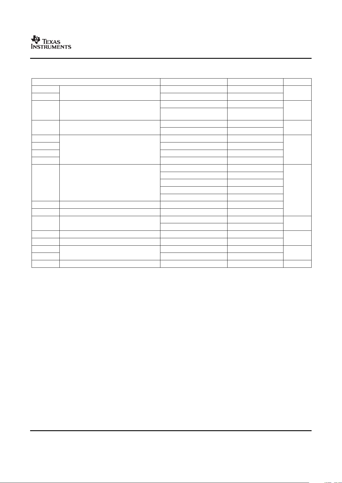
ABSOLUTE MAXIMUM RATINGS
(1)
UCD7230
SLUS741C – NOVEMBER 2006 – REVISED MARCH 2007
over operating free-air temperature range (unless otherwise noted)
PARAMETER CONDITION VALUE UNIT
V
DD
16
Supply voltage V
B
ST
SW + 16
I
DD
Quiescent 20
Supply current mA
Switching, TA= 25 ° C, V
DD
= 12
200
V
V
O
OUT1, BST -1 V to 36
Output gate drive voltage V V
OUT2 -1 V to VDD+0.3
I
OUT(sink)
OUT1 4.0
I
OUT(source)
OUT1 -2.0
Output gate drive current A
I
OUT(sink)
OUT2 4.0
I
OUT(source)
OUT2 -4.0
SW -1 to 20
CS+ -0.3 to 20
Analog inputs CSBIAS -0.3 to 16
POS, NEG -0.3 to 5.6 V
ILIM, DLY, I0 -0.3 to 3.6
Analog output A0 -0.3 to 3.6
Digital I/O’s IN, SRE, CLF -0.3 to 3.6
TA= 25 ° C (PWP-20 package) 2.67
Power dissipation W
TA= 25 ° C (QFN-20 package)
T
J
Junction operating temperature -55 to 150
° C
T
stg
Storage temperature -65 to 150
HBM Human body model 2000
ESD rating V
CDM Charged device model 500
Lead temperature (soldering, 10 sec) 300 ° C
(1) Stresses beyond those listed under “absolute maximum ratings” may cause permanent damage to the device. These are stress ratings
only and functional operation of the device at these or any other condition beyond those indicated is not implied. Exposure to absolute
maximum rated conditions for extended periods may affect device reliability. All voltages are with respect to GND. Currents are positive
into, negative out of the specified terminal. Consult company packaging information for thermal limitations and considerations of
packages.
5
www.ti.com
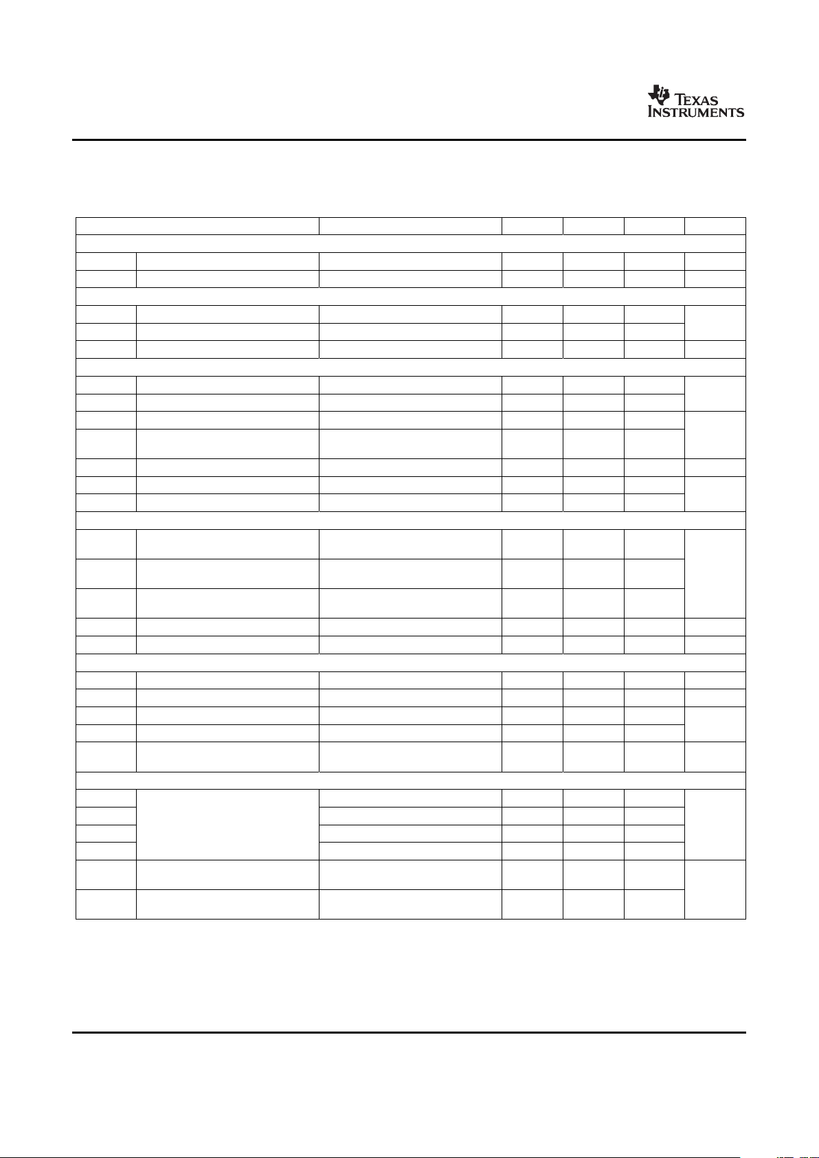
ELECTRICAL CHARACTERISTICS
UCD7230
SLUS741C – NOVEMBER 2006 – REVISED MARCH 2007
V
DD
= P
VDD
= 12 V, 4.7- µ F from V
DD
to A
GND
, 1 µ F from P
VDD
to P
GND
, 0.1 µ F from CSBIAS to AGND, 0.22 µ F from BST to
SW, TA= TJ= -40°C to +125°C, R
CS+
= 5 k Ω , R
DLY
= 50 k Ω over operating free-air temperature range (unless otherwise
noted).
PARAMETER TEST CONDITIONS MIN TYP MAX UNIT
SUPPLY
Supply current, off V
DD
= 4.2 V 500 700 µ A
Supply current Outputs not switching IN = LOW 5 8 mA
LOW-VOLTAGE UNDER-VOLTAGE LOCKOUT
VDD UVLO ON V
DD
rising 4.25 4.50 4.75
V
VDD UVLO OFF V
DD
falling 4.00 4.25 4.50
VDD UVLO hysteresis 100 250 400 mV
REFERENCE / EXTERNAL BIAS SUPPLY
3V3 initial set point TA= 25 ° C 3.267 3.3 3.333
V
3V3 over temperature 3.234 3.3 3.366
3V3 load regulation I
LOAD
= 1 mA to 10 mA, V
DD
= 5V 1 7
mV
V
DD
= 4.75 V to 12 V, I
LOAD
= 10
3V3 line regulation 3 10
mA
Short circuit current V
DD
= 4.75 V to 12 V 11 20 mA
3V3 OK threshold, ON 3.3 V rising 2.8 3 3.2
V
3V3 OK threshold, OFF 3.3 V falling 2.6 2.8 3.0
INPUT SIGNAL (IN)
Positive-going input threshold
INHigh 1.6 1.9 2.2
voltage
Negative-going input threshold
INLow 1.0 1.3 1.6 V
voltage
INHigh –
Input voltage hysteresis 0.4 0.6 0.8
INLow
Input resistance to AGND 50 100 150 k Ω
Frequency ceiling 2 MHz
CURRENT LIMIT (ILIM)
ILIM internal voltage setpoint I
LIM
=OPEN 0.47 0.50 0.53 V
ILIM input impedance 20 42 65 k Ω
CLF output high level I
LOAD
= 4 mA 2.7
V
CLF output low level I
LOAD
= 4 mA 0.6
Propagation delay from IN to reset 2nd IN rising to CLF falling after a
15 35 ns
CLF current limit event
CURRENT SENSE COMPARATOR (OUTPUT SENSE)
I
LIM
= open 40 50 60
I
LIM
= 3.3 V 80 100 120
CS threshold (POS - NEG) mV
I
LIM
= 0.75 V 60 75 90
I
LIM
= 0.25 V 15 25 35
Propagation delay from POS to
I
LIM
= open, CS = threshold + 60 mV 90
OUT1 falling
(1)
ns
Propagation delay from POS to
I
LIM
= open, CS = threshold + 60 mV 100
CLF
(1)
(1) As designed and characterized. Not 100% tested in production.
6
www.ti.com
UCD7230
SLUS741C – NOVEMBER 2006 – REVISED MARCH 2007
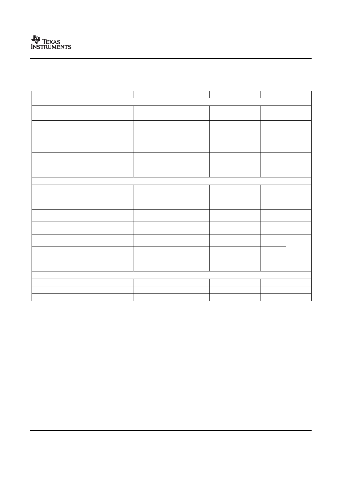
ELECTRICAL CHARACTERISTICS (continued)
V
DD
= P
VDD
= 12 V, 4.7- µ F from V
DD
to A
GND
, 1 µ F from P
VDD
to P
GND
, 0.1 µ F from CSBIAS to AGND, 0.22 µ F from BST to
SW, TA= TJ= -40°C to +125°C, R
CS+
= 5 k Ω , R
DLY
= 50 k Ω over operating free-air temperature range (unless otherwise
noted).
PARAMETER TEST CONDITIONS MIN TYP MAX UNIT
CURRENT SENSE COMPARATOR (INPUT SENSE)
R
DLY
= 24.3 k Ω (CSBIAS-CS+) 170 235 300
CS threshold mV
R
DLY
= 49.9 k Ω (CSBIAS-CS+) 90 114 140
R
DLY
= 24.3 k Ω , IN rising to OUT1,
120
IN falling to OUT2, VDD = 6 V
CS blanking time
(2)
ns
R
DLY
= 49.9 k Ω , IN rising to OUT1,
230
IN falling to OUT2, VDD = 6 V
R
DELAY
range
(2)
24.3 50.0 100.0 k Ω
Propagation delay from CS+ to
80
OUT1
(2)
CS = threshold + 60mV ns
Propagation delay from CS+ to
70
CLF
(2)
CURRENT SENSE AMP
I0 = OPEN; POS = NEG = 1.25 V;
V
OO
Output offset voltage -100 0 100 mV
measure AO - IO
I0 = FLOAT; V
POS
= 1.26 V; V
NEG
=
Closed loop dc gain 46 48 50 V/V
1.25 V, R
POS
= R
NEG
= 0
POS = 1.25 V, NEG = 1.29 V,R =
Input impedance 5.5 8.3 12 k Ω
(POS - NEG) / (I
POS
- I
NEG
)
V
CM(max)
is limited to (V
DD
-1.2V),
V
CM
Input Common Mode Voltage Range 0 5.6 V
R
POS
= 0
V
POS
= 1.2 V; V
NEG
= 1.3 V;
A0_Vol Minimum Output Voltage 0.15 0.3
A0_I
SINK
= 250 µ A
V
V
POS
=1.3 V; V
NEG
= 1.2 V; A0_
A0_Voh Maximum Output Voltage 3 3.1 3.5
I
SOURCE
= 500 µ A
I0 = FLOAT; V
POS
= V
NEG
= 0.8 V to
Input Bias Current, POS or NEG -2 30 µ A
5.0 V, R
POS
= R
NEG
= 0
ZERO CURRENT REFERENCE (IO)
Reference voltage Measured at I0 0.54 0.6 0.66 V
Input transition voltage With respect to IO reference 10 60 120 mV
I
O
Output impedance I
ZERO
= 0.6 V 10 15 21 k Ω
(2) As designed and characterized. Not 100% tested in production.
7
www.ti.com
UCD7230
SLUS741C – NOVEMBER 2006 – REVISED MARCH 2007
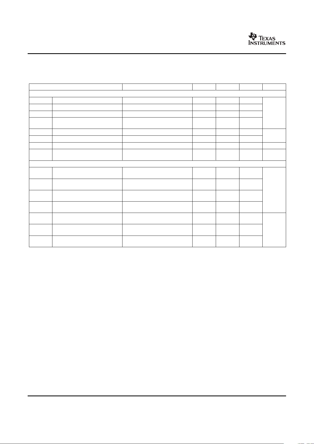
ELECTRICAL CHARACTERISTICS (continued)
V
DD
= P
VDD
= 12 V, 4.7- µ F from V
DD
to A
GND
, 1 µ F from P
VDD
to P
GND
, 0.1 µ F from CSBIAS to AGND, 0.22 µ F from BST to
SW, TA= TJ= -40°C to +125°C, R
CS+
= 5 k Ω , R
DLY
= 50 k Ω over operating free-air temperature range (unless otherwise
noted).
PARAMETER TEST CONDITIONS MIN TYP MAX UNIT
LOW-SIDE OUTPUT DRIVER (OUT2)
Source current
(3)
V
DD
= 12 V, IN = high, OUT2 = 5 V 2.2
Sink current
(3)
V
DD
= 12 V, IN = low, OUT2 = 5 V 3.5
A
Source current
(3)
V
DD
= 4.75 V, IN = high, OUT2 = 0 1.6
V
DD
= 4.75 V, IN = low, OUT2 =
Sink current
(3)
2
4.75 V
Rise time
(3)
C
LOAD
= 2.2 nF, V
DD
= 12 V 15
ns
Fall time
(3)
C
LOAD
= 2.2 nF, V
DD
= 12 V 15
Output with VDD <UVLO V
DD
= 1.0 V, Isink = 10 mA 0.8 1.2 V
Propagation delay from IN to C
LOAD
= 2.2 nF, IN rising, SW = 2.5
30 ns
OUT2
(3)
V, BST = PVDD = VDD = 12 V
HIGH-SIDE OUTPUT DRIVER (OUT1)
V
DD
= 12 V, BST = 12 V IN = High,
Source current
(3)
1.7
OUT1 = 5 V
V
DD
= 12 V, BST = 12 V IN = Low,
Sink current
(3)
3.5
OUT1 = 5 V
A
V
DD
= 4.75 V = BST = 4.75 V, IN =
Source current
(3)
1
High, OUT1 = 0
V
DD
= 4.75 V, BST = 4.75 V, IN =
Sink current
(3)
2.4
Low, OUT1 = 4.75 V
C
LOAD
= 2.2 nF OUT1 to SW, VDD
Rise time
(3)
20
= 12 V
C
LOAD
= 2.2 nF OUT1 to SW, V
DD
=
Fall time
(3)
15 ns
12 V
Propagation delay from IN to C
LOAD
= 2.2 nF, IN falling, SW = 2.5
30
OUT1
(3)
V, BST = PVDD = VDD = 12 V
(3) As designed and characterized. Not 100% tested in production.
8
 Loading...