

Page 1
www.ti.com
FEATURES DESCRIPTION
APPLICATIONS
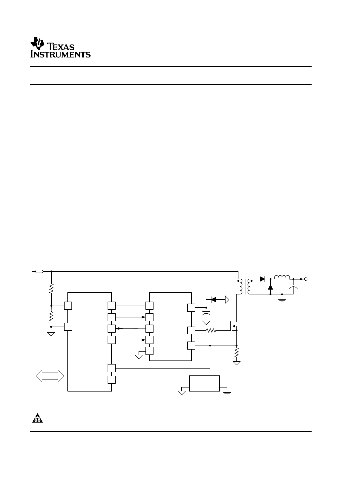
TYPICAL APPLICATION DIAGRAMS
14
12
8
OUT
CS
3
4
2
5
6
3V3
AGND
IN
CLF
ILIM
UCD7100PWP
Bias
Winding
VIN
VOUT
VDD
2
Isolation
Amplifier
PWMB
INT
Digital Controller
PWMA
VDD
AN2
AN3
AN1
AGND
Communication
UCD7100
SLUS651A – MARCH 2005 – REVISED MAY 2005
Digital Control Compatible Single Low-Side ± 4-A MOSFET Driver with Current Sense
• Adjustable Current Limit Protection
The UCD7100 is a member of the UCD7K family of
digital control compatible drivers for applications
• 3.3-V, 10-mA Internal Regulator
utilizing digital control techniques or applications re-
• DSP/µC Compatible Inputs
quiring fast local peak current limit protection.
• Single ± 4-A TrueDrive™ High Current Driver
The UCD7100 is a low-side ± 4-A high-current
• 10-ns Typical Rise and Fall Times with 2.2-nF
MOSFET gate driver. It allows the digital power
Loads
controllers such as UCD9110 or UCD9501 to
• 25-ns Input-to-Output Propagation Delay
interface to the power stage in single ended topologies. It provides a cycle-by-cycle current limit
• 25-ns Current Sense to Output Delay
function with programmable threshold and a digital
• Programmable Current Limit Threshold
output current limit flag which can be monitored by
• Digital Output Current Limit Flag
the host controller. With a fast 25-ns cycle-by-cycle
current limit protection, the driver can turn off the
• 4.5-V to 15-V Supply Voltage Range
power stage in the unlikely event that the digital
• Rated from -40 ° C to 105 ° C
system can not respond to a failure situation in time.
• Lead(Pb)-Free Packaging
For fast switching speeds, the UCD7100 output stage
uses the TrueDrive™ output architecture, which delivers rated current of ± 4 A into the gate of a
• Digitally Controlled Power Supplies
MOSFET during the Miller plateau region of the
• DC/DC Converters
switching transition. It also includes a 3.3-V, 10-mA
• Motor Controllers linear regulator to provide power to the digital control-
ler.
• Line Drivers
Please be aware that an important notice concerning availability, standard warranty, and use in critical applications of Texas
Instruments semiconductor products and disclaimers thereto appears at the end of this data sheet.
TrueDrive, PowerPAD are trademarks of Texas Instruments.
PRODUCTION DATA information is current as of publication date.
Copyright © 2005, Texas Instruments Incorporated
Products conform to specifications per the terms of the Texas
Instruments standard warranty. Production processing does not
necessarily include testing of all parameters.
Page 2
www.ti.com
DESCRIPTION (CONT.)
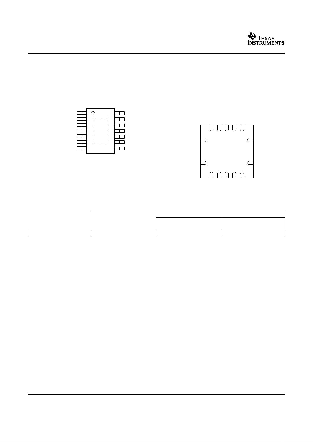
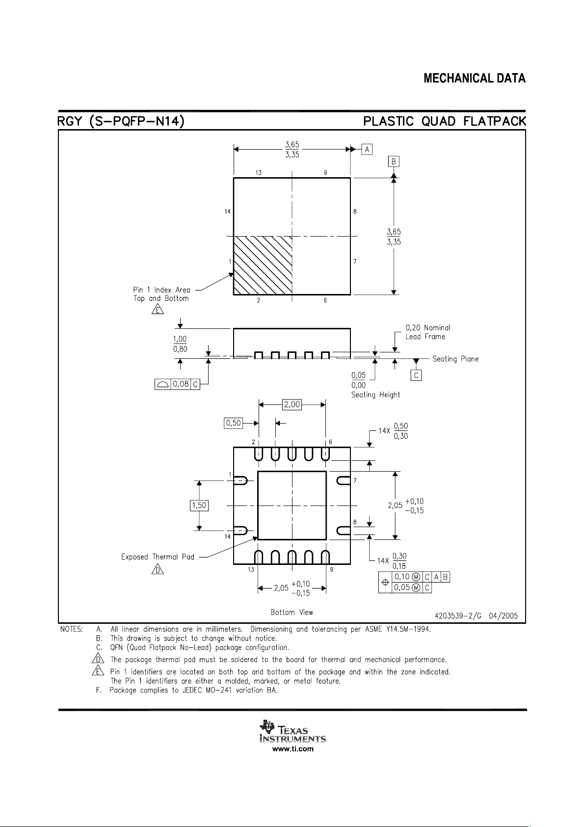
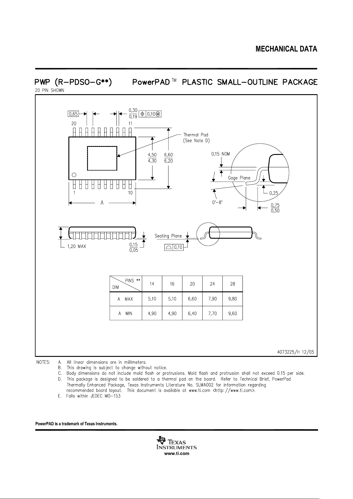
CONNECTION DIAGRAMS
1
2
3
4
5
6
7
14
13
12
11
10
9
8
PWP−14 PACKAGE
(TOP VIEW)
NC − No internal connection
VDD
IN
3V3
AGND
CLF
ILIM
NC
PVDD
PVDD
OUT
OUT
PGND
PGND
CS
VDD
PVDD
OUT
OUT
PGND
PGND
NC
RGY−14 PACKAGE
(BOTTOM VIEW)
1 7
IN
3V3
AGND
CLF
ILIM
1321231141059
6
14 8
CSPVDD
UCD7100
SLUS651A – MARCH 2005 – REVISED MAY 2005
The UCD7K driver family is compatible with standard 3.3 volt I/O ports of DSPs, Microcontrollers, or ASICs.
UCD7100 is offered in PowerPAD™ HTSSOP-14 or space-saving QFN-14 packages.
ORDERING INFORMATION
Packaged Devices
(1) (2) (3)
Temperature Range 110-V HV Startup Circuit
PowerPAD™ HTSSOP-14
QFN-14 (RGY)
(PWP)
-40 ° C to 105 ° C No UCD7100PWP UCD7100RGYT
(1) HTSSOP-14 (PWP) and QFN-14 (RGY) packages are available taped and reeled. Add R suffix to device type (e.g. UCD7100PWPR) to
order quantities of 2,000 devices per reel for the PWP package and 1,000 devices per reel for the RGY packages. Standard pack
quantity for the UCD7100RGYT is 250 devices.
(2) These products are packaged in Pb-Free and Green lead finish of Pd-Ni-Au which is compatible with MSL level 1 at 255 ° C to 260 ° C
peak reflow temperature to be compatible with either lead free or Sn/Pb soldering operations.
(3) QFN packaging is not yet available.
2
Page 3
www.ti.com
ABSOLUTE MAXIMUM RATINGS
(1) (2)
RECOMMENDED OPERATING CONDITIONS
UCD7100
SLUS651A – MARCH 2005 – REVISED MAY 2005
SYMBOL PARAMETER UCD7100 UNIT
V
DD
Supply Voltage 16
Quiescent 20
I
DD
Supply Current mA
Switching, TA= 25 ° C, TJ= 125 ° C, V
DD
= 12 V 200
Output Gate Drive Volt-
V
OUT
OUT -1 V to VDD V
age
I
OUT(sink)
4.0
Output Gate Drive Cur-
OUT A
rent
I
OUT(source)
-4.0
ISET, CS -0.3 to 3.6
Analog Input
ILIM -0.3 to 3.6 V
Digital I/O’s IN, CLF -0.3 to 3.6
Power Dissipation TA= 25 ° C, TJ= 125 ° C, (PWP-14) 2.67 W
T
J
Junction Operating Temperature -55 to 150
° C
T
str
Storage Temperature -65 to 150
HBM Human body model 2000
ESD Rating V
CDM Change device model 500
T
SOL
Lead Temperature (Soldering, 10 sec) +300 ° C
(1) Stresses beyond those listed under “absolute maximum ratings” may cause permanent damage to the device. These are stress ratings
only, and functional operation of the device at these or any other conditions beyond those indicated under “recommended operating
conditions” is not implied. Exposure to absolute-maximum-rated conditions for extended periods may affect device reliability.
(2) All voltages are with respect to GND. Currents are positive into, negative out of the specified terminal.
PARAMETER MIN TYP MAX UNIT
Supply Voltage, VDD 4.25 12 14.5 V
Supply bypass capacitance 1
µF
Reference bypass capacitance 0.22
Operating junction temperature -40 105 ° C
3
Page 4
www.ti.com
ELECTRICAL CHARACTERISTICS
UCD7100
SLUS651A – MARCH 2005 – REVISED MAY 2005
V
DD
= 12 V, 4.7-µF capacitor from V
DD
to GND, TA= TJ= -40 ° C to 105 ° C, (unless otherwise noted).
PARAMETER TEST CONDITIONS MIN TYP MAX UNIT
SUPPLY SECTION
Supply current, OFF V
DD
= 4.2 V 200 400 µA
Supply current Outputs not switching IN = LOW 1.5 2.5 mA
LOW VOLTAGE UNDER-VOLTAGE LOCKOUT
VDD UVLO ON 4.25 4.5 4.75
V
VDD UVLO OFF 4.05 4.25 4.45
VDD UVLO hysteresis 150 250 350 mV
REFERENCE / EXTERNAL BIAS SUPPLY
3V3 initial set point TA= 25 ° C 3.267 3.3 3.333
V
3V3 over temperature 3.234 3.3 3.366
3V3 load regulation I
LOAD
= 1 mA to 10 mA, VDD = 5 V 1 6.6
mV
3V3 line regulation VDD = 4.75 V to 12 V, I
LOAD
= 10 mA 1 6.6
Short circuit current VDD = 4.75 to 12 V 11 20 35 mA
3V3 OK threshold, ON 3.3 V rising 2.9 3.0 3.1
V
3V3 OK threshold, OFF 3.3 V falling 2.7 2.8 2.9
INPUT SIGNAL
HIGH, positive-going input threshold
1.65 2.08
voltage (VIT+)
LOW negative-going input threshold
1.16 1.5 V
voltage (VIT-)
Input voltage hysteresis, (VIT+ -
0.6 0.8
VIT-)
Frequency 2 MHz
CURRENT LIMIT (ILIM)
ILIM internal current limit threshold ILIM = OPEN 0.466 0.50 0.536 V
ILIM maximum current limit threshold I
LIM
= 3.3 V 0.975 1.025 1.075
V
ILIM current limit threshold I
LIM
= 0.75 V 0.700 0.725 0.750
ILIM minimum current limit threshold I
LIM
= 0.25 V 0.21 0.23 0.25 mV
CLF output high level CS > I
LIM
, I
LOAD
= -7 mA 2.64
V
CLF output low level CS ≤ I
LIM
, I
LOAD
= 7 mA 0.66
Propagation delay from IN to CLF IN rising to CLF falling after a current limit event 10 20 ns
CURRENT SENSE COMPARATOR
Bias voltage Includes CS comp offset 5 25 50 mV
Input bias current –1 uA
Propagation delay from CS to OUTx I
LIM
= 0.5 V, measured on OUTx, CS = threshold + 60 mV 25 40
ns
Propagation delay from CS to CLF I
LIM
= 0.5 V, measured on CLF, CS = threshold + 60 mV 25 50
CURRENT SENSE DISCHARGE TRANSISTOR
Discharge resistance IN = low, resistance from CS to AGND 10 35 75 Ω
4
Page 5
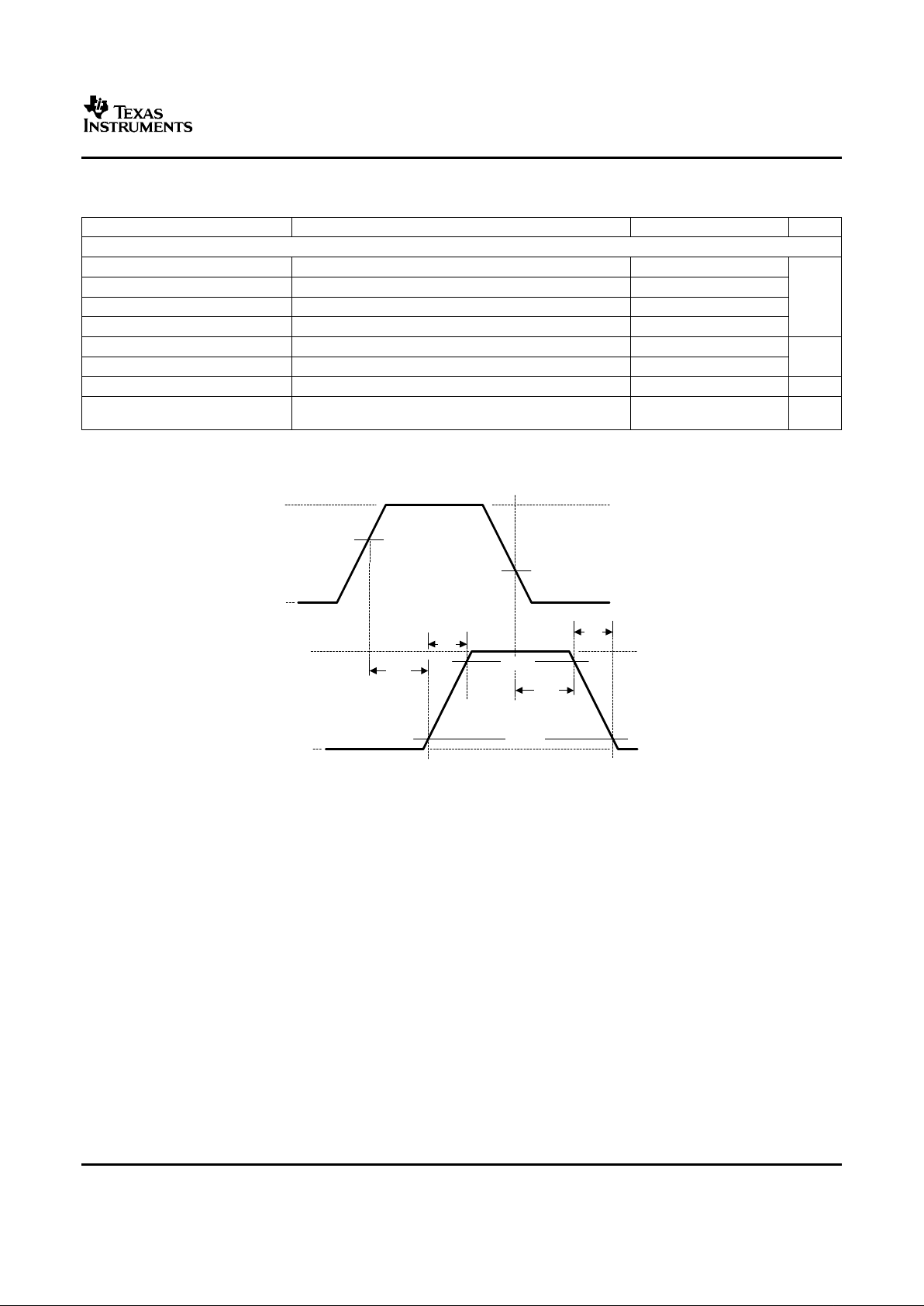
www.ti.com
VIT−
10%
90%
INPUT
OUTPUT
VIT+
t
D1
t
F
t
F
t
D2
UCD7100
SLUS651A – MARCH 2005 – REVISED MAY 2005
ELECTRICAL CHARACTERISTICS (continued)
V
DD
= 12 V, 4.7-µF capacitor from V
DD
to GND, TA= TJ= -40 ° C to 105 ° C, (unless otherwise noted).
PARAMETER TEST CONDITIONS MIN TYP MAX UNIT
OUTPUT DRIVERS
Source current
(1)
V
DD
= 12 V, IN = high, OUT = 5 V 4
Sink current
(1)
V
DD
= 12 V, IN = low, OUT = 5 V 4
A
Source current
(1)
V
DD
= 4.75 V, IN = high, OUT = 0 2
Sink current
(1)
V
DD
= 4.75 V, IN = low, OUT = 4.75 V 3
Rise time, t
R
(1)
C
LOAD
= 2.2 nF, V
DD
= 12 V 10 20
ns
Fall time, t
F
(1)
C
LOAD
= 2.2 nF, V
DD
= 12 V 10 15
Output with V
DD
< UVLO V
DD
= 1.0 V, I
SINK
= 10 mA 0.8 1.2 V
Propagation delay from IN to OUTx,
C
LOAD
= 2.2 nF, V
DD
= 12 V, CLK rising 20 35 ns
t
D1
(1) Ensured by design. Not 100% tested in production.
NOTE:
The 10% and 90% thresholds depict the dynamics of the bipolar output devices that
dominate the power MOSFET transition through the Miller regions of operation.
5
Page 6
www.ti.com
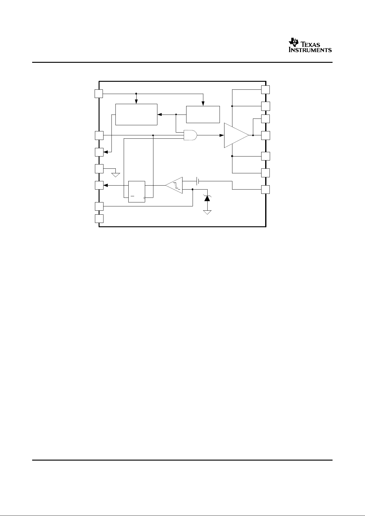
FUNCTIONAL BLOCK DIAGRAM
2
7
4
3
5
6
3V3 Regulator
&
Reference
UVLO
12
14
11
1
10
9
8
PVDD
N/C
3V3
IN
AGND
CLF
ILIM
OUT
OUT
PGND
PGND
CS
+
13
PVDD
VDD
+
25 mV
SDQ
Q R
UCD7100
SLUS651A – MARCH 2005 – REVISED MAY 2005
Figure 1. UCD7100
6
Page 7
www.ti.com
TERMINAL FUNCTIONS
UCD7100
SLUS651A – MARCH 2005 – REVISED MAY 2005
UCD7100
PIN
I/O FUNCTION
HTSSOP DFN-14
NAME
-14 PIN # PIN #
Supply input pin to power the driver. The UCD7K devices accept an input range of 4.25 V to
1 1 VDD I
15 V. Bypass the pin with at least 4.7 µF of capacitance.
The IN pin is a high impedance digital input capable of accepting 3.3-V logic level signals up
2 2 IN I to 2 MHz. There is an internal Schmitt trigger comparator which isolates the internal circuitry
from any external noise.
Regulated 3.3-V rail. The onboard linear voltage regulator is capable of sourcing up to 10 mA
3 3 3V3 O
of current. Place 0.22-µF of ceramic capacitance from the pin to ground.
4 4 AGND - Analog ground return.
Current limit flag. When the CS level is greater than the ILIM voltage minus 25 mV, the output
5 5 CLF O of the driver is forced low and the current limit flag (CLF) is set high. The CLF signal is
latched high until the UCD7K device receives the next rising edge on the IN pin.
Current limit threshold set pin. The current limit threshold can be set to any value between
6 6 ILIM I
0.25 V and 1.0 V.
7 7 NC - No Connection.
Current sense pin. Fast current limit comparator connected to the CS pin is used to protect
8 8 CS I
the power stage by implementing cycle-by-cycle current limiting.
Power ground return. Connect the two PGNDs together. These ground pins should be
9 9 PGND -
connected very closely to the source of the power MOSFET.
Power ground return. Connect the two PGNDs together. These ground pins should be
10 10 PGND -
connected very closely to the source of the power MOSFET.
11 11 OUT O The high-current TrueDrive™ driver output. Connect the two OUT pins together.
12 12 OUT O The high-current TrueDrive™ driver output. Connect the two OUT pins together.
Supply pin provides power for the output drivers. It is not connected internally to the VDD
13 13 PVDD I
supply rail. Connect the two PVDD pins together.
Supply pin provides power for the output drivers. It is not connected internally to the VDD
14 14 PVDD I
supply rail. Connect the two PVDD pins together.
7
Page 8

www.ti.com
APPLICATION INFORMATION
Supply
Current Sensing and Protection
Reference / External Bias Supply
Input
UCD7100
SLUS651A – MARCH 2005 – REVISED MAY 2005
The UCD7100 is part of a family of digital compatible If limiting the rise or fall times to the power device is
drivers targeting applications utilizing digital control desired, then an external resistance can be added
techniques or applications that require local fast peak between the output of the driver and the load device,
current limit protection. which is generally a power MOSFET gate. The
external resistor may also help remove power dissipation from the package.
The UCD7K devices accept an input range of 4.5 V
to 15 V. The device has an internal precision linear
regulator that produces the 3V3 output from this VDD A very fast current limit comparator connected to the
input. A separate pin, PVDD, not connected internally CS pin is used to protect the power stage by
to the VDD supply rail provides power for the output implementing cycle-by-cycle current limiting.
drivers. In all applications the same bus voltage
The current limit threshold is equal to the lesser of
supplies the two pins. It is recommended that a low
the positive inputs at the current limit comparator.
value of resistance be placed between the two pins
The current limit threshold can be set to any value
so that the local capacitance on each pin forms low
between 0.25 V and 1.0 V by applying the desired
pass filters to attenuate any switching noise that may
threshold voltage to the current limit (ILIM) pin. When
be on the bus.
the CS level is greater than the ILIM voltage minus
Although quiescent VDD current is low, total supply 25 mV, the output of the driver is forced low and the
current will be higher, depending on the gate drive current limit flag (CLF) is set high. The CLF signal is
output current required by the switching frequency. latched high until the UCD7K device receives the
Total V
DD
current is the sum of quiescent V
DD
current next rising edge on the IN pin.
and the average OUT current. Knowing the operating
When the CS voltage is below ILIM, the driver output
frequency and the MOSFET gate charge (Q
G
), aver-
will follow the PWM input. The CLF digital output flag
age OUT current can be calculated from:
can be monitored by the host controller to determine
I
OUT
= Q
G
x f, where f is frequency. when a current limit event occurs and to then apply
the appropriate algorithm to obtain the desired current
For high-speed circuit performance, a V
DD
bypass
limit profile.
capacitor is recommended to prevent noise problems.
A 4.7-µF ceramic capacitor should be located close to One of the main benefits of this local protection
the V
DD
to ground connection. A larger capacitor with feature is that the UCD7K devices can protect the
relatively low ESR should be connected to the PVDD power stage if the software code in the digital
pin, to help deliver the high current peaks to the load. controller becomes corrupted and hangs up. If the
The capacitors should present a low impedance controller’s PWM output stays high, the local current
characteristic for the expected current levels in the sense circuit will turn off the driver output when an
driver application. The use of surface mount over-current condition occurs. The system would
components for all bypass capacitors is highly rec- likely go into a retry mode because; most DSP and
ommended. microcontrollers have on-board watchdog, brown-out,
and other supervisory peripherals to restart the device in the event that it is not operating properly. But
these peripherals typically do not react fast enough to
All devices in the UCD7K family are capable of
save the power stage. The UCD7K’s local current
supplying a regulated 3.3-V rail to power various
limit comparator provides the required fast protection
types of external loads such as a microcontroller or
for the power stage.
an ASIC. The onboard linear voltage regulator is
capable of sourcing up to 10 mA of current. For The CS threshold is 25 mV below the ILIM voltage.
normal operation, place a minimum of 0.22 µF of This way, if the user attempts to command zero
ceramic capacitance from the reference pin to current (I
LIM
< 25 mV) while the CS pin is at ground,
ground. for example at start-up, the CLF flag latches high until
the IN pin receives a pulse. At start-up it is necessary
to ensure that the ILIM pin always greater than the
CS pin for the handshaking to work as described
The IN pin is a high impedance digital input capable
below. If for any reason the CS pin comes to within
of accepting 3.3-V logic level signals up to 2 MHz.
25 mV of the ILIM pin during start-up, then the CLF
There is an internal Schmitt Trigger comparator which
isolates the internal circuitry from any external noise.
8
Page 9

www.ti.com
Handshaking Drive Current and Power Requirements
Driver Output
E
1
2
CV
2
(1)
P
1
2
CV2 f
(2)
Source/Sink Capabilities During Miller Plateau
UCD7100
SLUS651A – MARCH 2005 – REVISED MAY 2005
flag is latched high and the digital controller must poll drain voltage is swinging between the voltage levels
the UCD7K device, by sending it a narrow IN pulse. If dictated by the power topology, requiring the chargthe fault condition is not present the IN pulse resets ing/discharging of the drain-gate capacitance with
the CLF signal to low indicating that the UCD7K current supplied or removed by the driver device. See
device is ready to process power pulses. Reference [1]
The UCD7K family of devices have a built-in hand- The UCD7K family of drivers can deliver high current
shaking feature to facilitate efficient start-up of the into a MOSFET gate for a period of several hundred
digitally controlled power supply. At start-up the CLF nanoseconds. High peak current is required to turn
flag is held high until all the internal and external the device ON quickly. Then, to turn the device OFF,
supply voltages of the UCD7K device are within their the driver is required to sink a similar amount of
operating range. Once the supply voltages are within current to ground. This repeats at the operating
acceptable limits, the CLF goes low and the device frequency of the power device. A MOSFET is used in
will process input drive signals. The micro-controller this discussion because it is the most common type
should monitor the CLF flag at start-up and wait for of switching device used in high frequency power
the CLF flag to go LOW before sending power pulses conversion equipment.
to the UCD7K device.
Reference [1] discusses the current required to drive
a power MOSFET and other capacitive-input
switching devices.
The high-current output stage of the UCD7K device
When a driver device is tested with a discrete,
family is capable of supplying ± 4-A peak current
capacitive load it is a fairly simple matter to calculate
pulses and swings to both VDD and GND. The driver
the power that is required from the bias supply. The
outputs follows the state of the IN pin provided that
energy that must be transferred from the bias supply
the VDD and 3V3 voltages are above their respective
to charge the capacitor is given by:
under-voltage lockout threshold.
The drive output utilizes Texas Instruments’
TrueDrive™ architecture, which delivers rated current
where C is the load capacitor and V is the bias
into the gate of a MOSFET when it is most needed
voltage feeding the driver.
during the Miller plateau region of the switching
transition providing efficiency gains.
There is an equal amount of energy transferred to
ground when the capacitor is discharged. This leads
TrueDrive™ consists of pullup/ pulldown circuits
to a power loss given by the following:
using bipolar and MOSFET transistors in parallel. The
peak output current rating is the combined current
from the bipolar and MOSFET transistors. The output
resistance is the R
DS(on)
of the MOSFET transistor
where f is the switching frequency.
when the voltage on the driver output is less than the
saturation voltage of the bipolar transistor. This hybrid
This power is dissipated in the resistive elements of
output stage also allows efficient current sourcing at
the circuit. Thus, with no external resistor between
low supply voltages.
the driver and gate, this power is dissipated inside the
driver. Half of the total power is dissipated when the
Each output stage also provides a very low im-
capacitor is charged, and the other half is dissipated
pedance to overshoot and undershoot due to the
when the capacitor is discharged. An actual example
body diode of the external MOSFET. This means that
using the conditions of the previous gate drive
in many cases, external-schottky-clamp diodes are
waveform should help clarify this.
not required.
Large power MOSFETs present a large load to the
control circuitry. Proper drive is required for efficient,
reliable operation. The UCD7K drivers have been
optimized to provide maximum drive to a power
MOSFET during the Miller plateau region of the
switching transition. This interval occurs while the
9
Page 10

www.ti.com
Thermal Information
P 10 nF 122 300 kHz 0.432 W
(3)
I
P
V
0.432 W
12 V
0.036 A
(4)
Circuit Layout Recommendations
P C V2 f QG V f
(5)
UCD7100
SLUS651A – MARCH 2005 – REVISED MAY 2005
With V
DD
= 12 V, C
LOAD
= 10 nF, and f = 300 kHz, the
power loss can be calculated as:
The useful range of a driver is greatly affected by the
drive power requirements of the load and the thermal
characteristics of the device package. In order for a
With a 12-V supply, this would equate to a current of:
power driver to be useful over a particular temperature range the package must allow for the efficient
removal of the heat produced while keeping the
junction temperature within rated limits. The UCD7K
The actual current measured from the supply was
family of drivers is available in PowerPAD™ TSSOP
0.037 A, and is very close to the predicted value. But,
and QFN/DFN packages to cover a range of appli-
the I
DD
current that is due to the device internal
cation requirements. Both have the exposed pads to
consumption should be considered. With no load the
relieve thermal dissipation from the semiconductor
device current drawn is 0.0027 A. Under this con-
junction.
dition the output rise and fall times are faster than
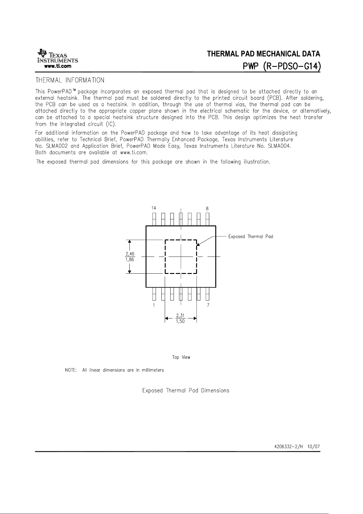
with a load. This could lead to an almost insignificant,
As illustrated in Reference [2], the PowerPAD™
yet measurable current due to cross-conduction in the
packages offer a leadframe die pad that is exposed at
output stages of the driver. However, these small
the base of the package. This pad is soldered to the
current differences are buried in the high frequency
copper on the PC board (PCB) directly underneath
switching spikes, and are beyond the measurement
the device package, reducing the Θ
JC
down to
capabilities of a basic lab setup. The measured
4.7 ° C/W. The PC board must be designed with
current with 10-nF load is close to the value ex-
thermal lands and thermal vias to complete the heat
pected.
removal subsystem, as summarized in Reference [3].
The switching load presented by a power MOSFET
Note that the PowerPAD™ is not directly connected
can be converted to an equivalent capacitance by
to any leads of the package. However, it is electrically
examining the gate charge required to switch the
and thermally connected to the substrate which is the
device. This gate charge includes the effects of the
ground of the device.
input capacitance plus the added charge needed to
swing the drain of the device between the ON and
OFF states. Most manufacturers provide specifi-
In a power driver operating at high frequency, it is a
cations that provide the typical and maximum gate
significant challenge to get clean waveforms without
charge, in nC, to switch the device under specified
much overshoot/undershoot and ringing. The low
conditions. Using the gate charge Q
G
, one can
output impedance of these drivers produces
determine the power that must be dissipated when
waveforms with high di/dt. This tends to induce
charging a capacitor. This is done by using the
ringing in the parasitic inductances. Utmost care must
equivalence Q
G
= C
EFF
x V to provide the following
be used in the circuit layout. It is advantageous to
equation for power:
connect the driver IC as close as possible to the
leads. The driver device layout has the analog ground
on the opposite side of the output, so the ground
This equation allows a power designer to calculate
should be connected to the bypass capacitors and
the bias power required to drive a specific MOSFET
the load with copper trace as wide as possible. These
gate at a specific bias voltage.
connections should also be made with a small enclosed loop area to minimize the inductance.
10
Page 11

www.ti.com
14
UCD91xx
with
CLA
Peripheral
1
12
8
PVDD
OUT
CS
10
PGND
3
4
2
5
6
3V3
AGND
IN
CLF
ILIM
7
2
UCD7100PWP
Bias
Winding
VIN
VOUT
VDS
CS
FB
CS
VDS
COMMUNICATION
(Programming & Status Reporting)
Bias Supply
11OUT
9
PGND
13
PVDD
VDD
NC
2
Isolation
Amplifier
2
1
UCD7100
SLUS651A – MARCH 2005 – REVISED MAY 2005
Figure 2. Isolated Forward Converter
11
Page 12

www.ti.com
14
UCD9501
Digital
1
12
8
PVDD
OUT
CS
10
PGND
3
4
2
5
6
3V3
AGND
IN
CLF
ILIM
7
UCD7100PWP
VOUT
VDS
CS
FB
CS
VDS
COMMUNICATION
(Programming & Status Reporting)
Bias
Supply
11
OUT
9
PGND
13
PVDDVDD
NC
Signal
Conditioning
Amplifier
~
~
+−
VAC
PFC_ISENSE
Signal
Conditioning
Amplifier
Controller
UCD7100
SLUS651A – MARCH 2005 – REVISED MAY 2005
Figure 3. PFC Boost Front-End Power Supply
12
Page 13

www.ti.com
TYPICAL CHARACTERISTICS
−50 50 125−25 0 25 75 100
3.24
3.26
3.28
3.30
3.32
3.34
3.36
t − Temperature − °C
3V3 − Reference Voltage − V
−50 50
5.0
4.5
2.5
2.0
1.5
0.5
0.0
−25 0 25 75 100
4.0
1.0
3.5
3.0
UVLO on
UVLO on
UVLO on
t − Temperature − °C
125
V
UVLO
− UVLO Thresholds − V
−50 50 125−25 0 25 75 100
20.0
20.5
21.0
21.5
22.0
22.5
23.0
t − Temperature − °C
I
SHORT_CKT
− Short Circuit Current − mA
VDD = 4.75 V
VDD = 12 V
−50 50 125−25 0 25 75 100
0.0
0.5
1.0
1.5
2.0
2.5
TJ − Temperature − °C
V
INPUT
− Input Voltage − V
Input Rising
Input Falling
UCD7100
SLUS651A – MARCH 2005 – REVISED MAY 2005
UVLO THRESHOLDS 3V3 REFERENCE VOLTAGE
vs vs
TEMPERATURE TEMPERATURE
Figure 4. Figure 5.
3V3 SHORT CIRCUIT CURRENT INPUT THRESHOLDS
vs vs
TEMPERATURE TEMPERATURE
Figure 6. Figure 7.
13
Page 14

www.ti.com
5
15
25
35
45
55
65
5 7.5 10 12.5 15
VDD − Supply Voltage − V
t
R
− Rise Time − ns
C
LOAD
= 10 nF
C
LOAD
= 4.7 nF
C
LOAD
= 2.2 nF
C
LOAD
= 1 nF
−50 50 125−25 0 25 75 100
0.0
2.0
4.0
6.0
8.0
10.0
12.0
14.0
16.0
18.0
TJ − Temperature − °C
t
R,
t
F
− Rise and Fall Times − ns
tR = Rise Time
tF = Fall Time
0
5
10
15
20
5 7.5 10 12.5 15
VDD − Supply Voltage − V
t
PD
− Propagation Delay, Rising − ns
C
LOAD
= 10 nF
C
LOAD
= 4.7 nF
C
LOAD
= 2.2 nF
C
LOAD
= 1 nF
5
10
15
20
25
30
35
40
45
5 7.5 10 12.5 15
VDD − Supply Voltage − V
t
F
− Fall Time − ns
C
LOAD
= 10 nF
C
LOAD
= 4.7 nF
C
LOAD
= 2.2 nF
C
LOAD
= 1 nF
UCD7100
SLUS651A – MARCH 2005 – REVISED MAY 2005
TYPICAL CHARACTERISTICS (continued)
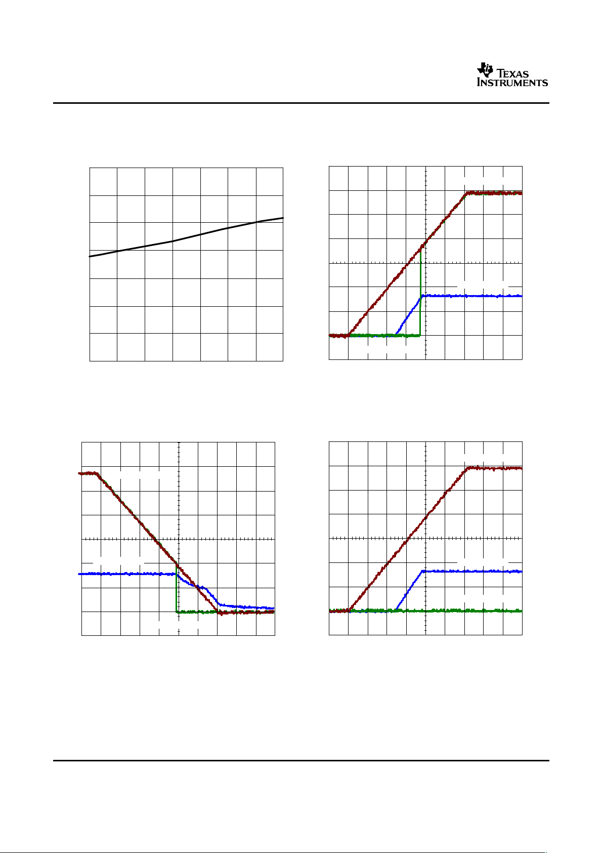
OUTPUT RISE TIME AND FALL TIME RISE TIME
vs vs
TEMPERATURE (V
DD
= 12 V) SUPPLY VOLTAGE
Figure 8. Figure 9.
FALL TIME PROPAGATION DELAY RISING
vs vs
SUPPLY VOLTAGE SUPPLY VOLTAGE
Figure 10. Figure 11.
14
Page 15
www.ti.com
5
10
15
20
25
5 7.5 10 12.5 15
VDD − Supply Voltage − V
t
PD
− Propagation Delay, Falling − ns
C
LOAD
= 10 nF
C
LOAD
= 4.7 nF
C
LOAD
= 2.2 nF
C
LOAD
= 1 nF
−50 50 125−25 0 25 75 100
0.46
0.47
0.48
0.49
0.50
0.51
0.52
0.53
0.54
TJ − Temperature − °C
V
CS
− Current Limit Threshold − V
−50 50−25 0 25 75 100
0
5
10
15
20
25
30
35
40
45
50
TJ − Temperature − °C
t
PD
− CS to CLF Propagation Delay − ns
125
−50 50 125−25 0 25 75 100
0
5
10
15
20
25
30
35
40
TJ − Temperature − °C
t
PD
− CS to OUTx Propagation Delay − ns
UCD7100
SLUS651A – MARCH 2005 – REVISED MAY 2005
TYPICAL CHARACTERISTICS (continued)
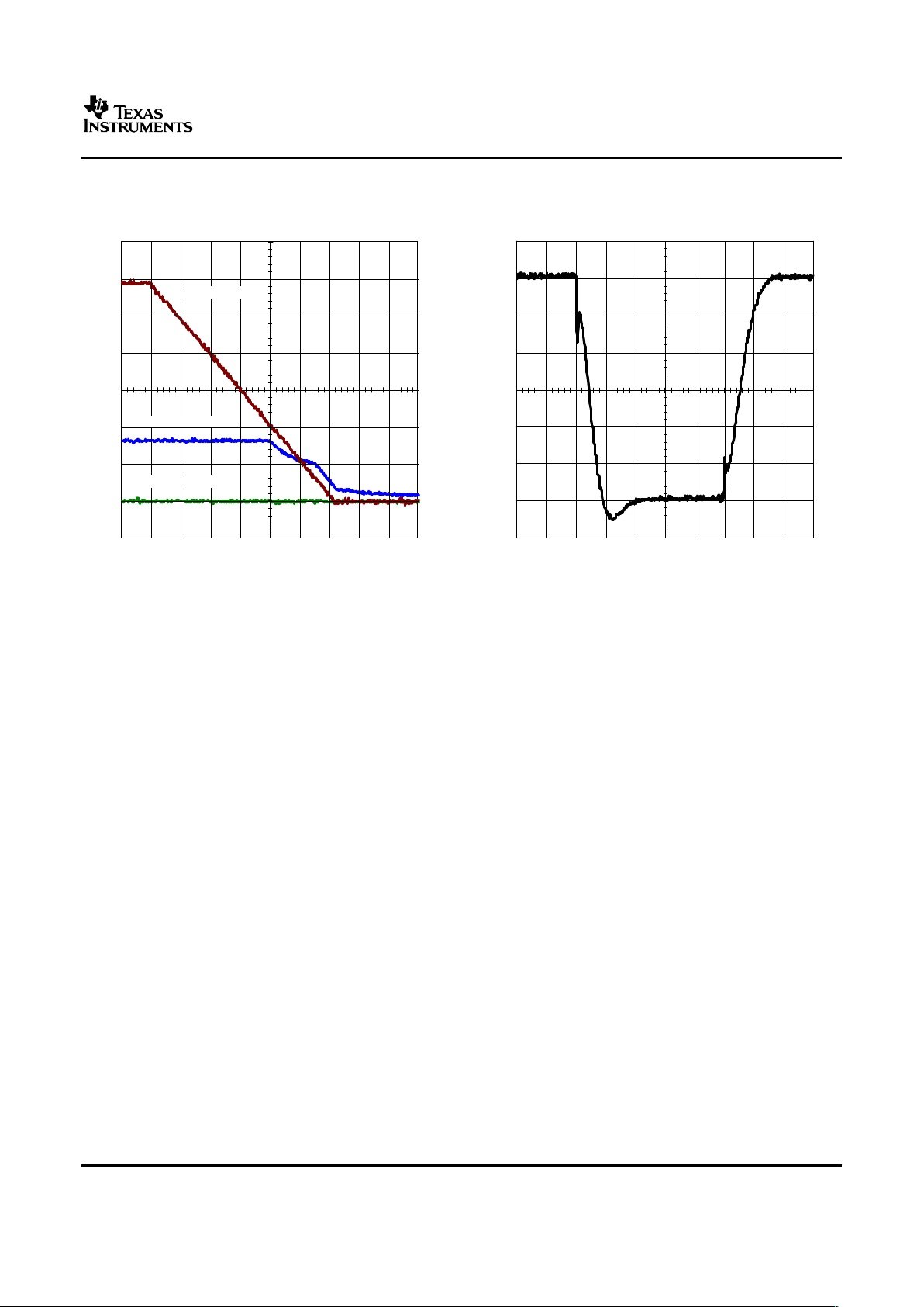
PROPAGATION DELAY FALLING DEFAULT CURRENT LIMIT THRESHOLD
vs vs
SUPPLY VOLTAGE TEMPERATURE
Figure 12. Figure 13.
CS TO OUTx PROPAGATION DELAY CS TO CLF PROPAGATION DELAY
vs vs
TEMPERATURE TEMPERATURE
Figure 14. Figure 15.
15
Page 16
www.ti.com
t − Time − 40 µs/div
VDD (2 V/div)
3V3 (2 V/div)
OUTx (2 V/div)
−50 50 125−25 0 25 75 100
0
5
10
15
20
25
30
35
TJ − Temperature − °C
t
PD
− Propagation Delay − ns
t − Time − 40 µs/div
VDD (2 V/div)
3V3 (2 V/div)
OUTx (2 V/div)
t − Time − 40 µs/div
VDD (2 V/div)
3V3 (2 V/div)
OUTx (2 V/div)
UCD7100
SLUS651A – MARCH 2005 – REVISED MAY 2005
TYPICAL CHARACTERISTICS (continued)
IN TO OUT PROPAGATION DELAY
vs
TEMPERATURE START-UP BEHAVIOR AT V
DD
= 12 V (INPUT TIED TO 3V3)
Figure 16. Figure 17.
SHUT DOWN BEHAVIOR AT V
DD
= 12 V (INPUT TIED TO START-UP BEHAVIOR AT V
DD
= 12 V (INPUT SHORTED
3V3) TO GND)
Figure 18. Figure 19.
16
Page 17
www.ti.com
t − Time − 40 ns/div
Output Voltage − 2 V/div
t − Time − 40 µs/div
VDD (2 V/div)
3V3 (2 V/div)
OUTx (2 V/div)
UCD7100
SLUS651A – MARCH 2005 – REVISED MAY 2005
TYPICAL CHARACTERISTICS (continued)
SHUT DOWN BEHAVIOR AT V
DD
= 12 V (INPUT SHORTED OUTPUT RISE AND FALL TIME (V
DD
= 12 V, C
LOAD
= 10
TO GND) NF)
Figure 20. Figure 21.
17
Page 18

www.ti.com
REFERENCES
RELATED PRODUCTS
REVISION HISTORY
UCD7100
SLUS651A – MARCH 2005 – REVISED MAY 2005
1. Power Supply Seminar SEM–1400 Topic 2: Design And Application Guide For High Speed MOSFET Gate
Drive Circuits, by Laszlo Balogh, Texas Instruments Literature No. SLUP133.
2. Technical Brief, PowerPad Thermally Enhanced Package, Texas Instruments Literature No. SLMA002
3. Application Brief, PowerPAD Made Easy, Texas Instruments Literature No. SLMA004
PRODUCT DESCRIPTION FEATURES
UCD7200 Dual Low Side ± 4-A Drivers with Independent CS 3V3, CS
(1) (2)
UCD7201 Dual Low Side ± 4-A Drivers with Common CS 3V3, CS
(1) (2)
UCD7230 ± 4A Synchronous Buck Driver with CS 3V3, CS
(1) (2)
Single Low Side ± 4-A Driver with CS and 110-V High Voltage Startup 3V3, CS,
UCD7500
HVS110
(1) (2) (3)
Dual Low Side ± 4-A Drivers with Independent CS and 110-V High Voltage Startup 3V3, CS,
UCD7600
HVS110
(1) (2) (3)
Dual Low Side ± 4-A Drivers with Common CS and 110-V High Voltage Startup 3V3, CCS,
UCD7601
HVS110
(1) (4) (3)
UCD9110 Digital Power Controller for High Performance Single-loop Applications
UCD9501 Digital Power Controller for High Performance Multi-loop Applications
(1) 3V3 = 3.3V linear regulator.
(2) CS = current sense and current limit function.
(3) HVS110 = 110-V high voltage startup circuit.
(4) CCS = common current sense and current limit function.
DATE REVISION CHANGE DESCRIPTION
3/4/05 SLUS651 Initial release
18
Page 19
PACKAGING INFORMATION
Orderable Device Status
(1)
Package
Type
Package
Drawing
Pins Package
Qty
Eco Plan
(2)
Lead/Ball Finish MSL Peak Temp
(3)
UCD7100PWP ACTIVE HTSSOP PWP 14 90 Green (RoHS &
no Sb/Br)
CU NIPDAU Level-2-260C-1 YEAR
UCD7100PWPG4 ACTIVE HTSSOP PWP 14 90 Green (RoHS &
no Sb/Br)
CU NIPDAU Level-2-260C-1 YEAR
UCD7100PWPR ACTIVE HTSSOP PWP 14 2000 Green (RoHS &
no Sb/Br)
CU NIPDAU Level-2-260C-1 YEAR
UCD7100PWPRG4 ACTIVE HTSSOP PWP 14 2000 Green (RoHS &
no Sb/Br)
CU NIPDAU Level-2-260C-1 YEAR
UCD7100RGYR PREVIEW QFN RGY 14 1000 TBD Call TI Call TI
(1)
The marketing status values are defined as follows:
ACTIVE: Product device recommended for new designs.
LIFEBUY: TI has announced that the device will be discontinued, and a lifetime-buy period is in effect.
NRND: Not recommended for new designs. Device is in production to support existing customers, but TI does not recommend using this part in
a new design.
PREVIEW: Device has been announced but is not in production. Samples may or may not be available.
OBSOLETE: TI has discontinued the production of the device.
(2)
Eco Plan - The planned eco-friendly classification: Pb-Free (RoHS), Pb-Free (RoHS Exempt), or Green (RoHS & no Sb/Br) - please check
http://www.ti.com/productcontent for the latest availability information and additional product content details.
TBD: The Pb-Free/Green conversion plan has not been defined.
Pb-Free (RoHS): TI's terms "Lead-Free" or "Pb-Free" mean semiconductor products that are compatible with the current RoHS requirements
for all 6 substances, including the requirement that lead not exceed 0.1% by weight in homogeneous materials. Where designed to be soldered
at high temperatures, TI Pb-Free products are suitable for use in specified lead-free processes.
Pb-Free (RoHS Exempt): This component has a RoHS exemption for either 1) lead-based flip-chip solder bumps used between the die and
package, or 2) lead-based die adhesive used between the die and leadframe. The component is otherwise considered Pb-Free (RoHS
compatible) as defined above.
Green (RoHS & no Sb/Br): TI defines "Green" to mean Pb-Free (RoHS compatible), and free of Bromine (Br) and Antimony (Sb) based flame
retardants (Br or Sb do not exceed 0.1% by weight in homogeneous material)
(3)
MSL, Peak Temp. -- The Moisture Sensitivity Level rating according to the JEDEC industry standard classifications, and peak solder
temperature.
Important Information and Disclaimer:The information provided on this page represents TI's knowledge and belief as of the date that it is
provided. TI bases its knowledge and belief on information provided by third parties, and makes no representation or warranty as to the
accuracy of such information. Efforts are underway to better integrate information from third parties. TI has taken and continues to take
reasonable steps to provide representative and accurate information but may not have conducted destructive testing or chemical analysis on
incoming materials and chemicals. TI and TI suppliers consider certain information to be proprietary, and thus CAS numbers and other limited
information may not be available for release.
In no event shall TI's liability arising out of such information exceed the total purchase price of the TI part(s) at issue in this document sold by TI
to Customer on an annual basis.
PACKAGE OPTION ADDENDUM
www.ti.com
5-Feb-2007
Addendum-Page 1
Page 20
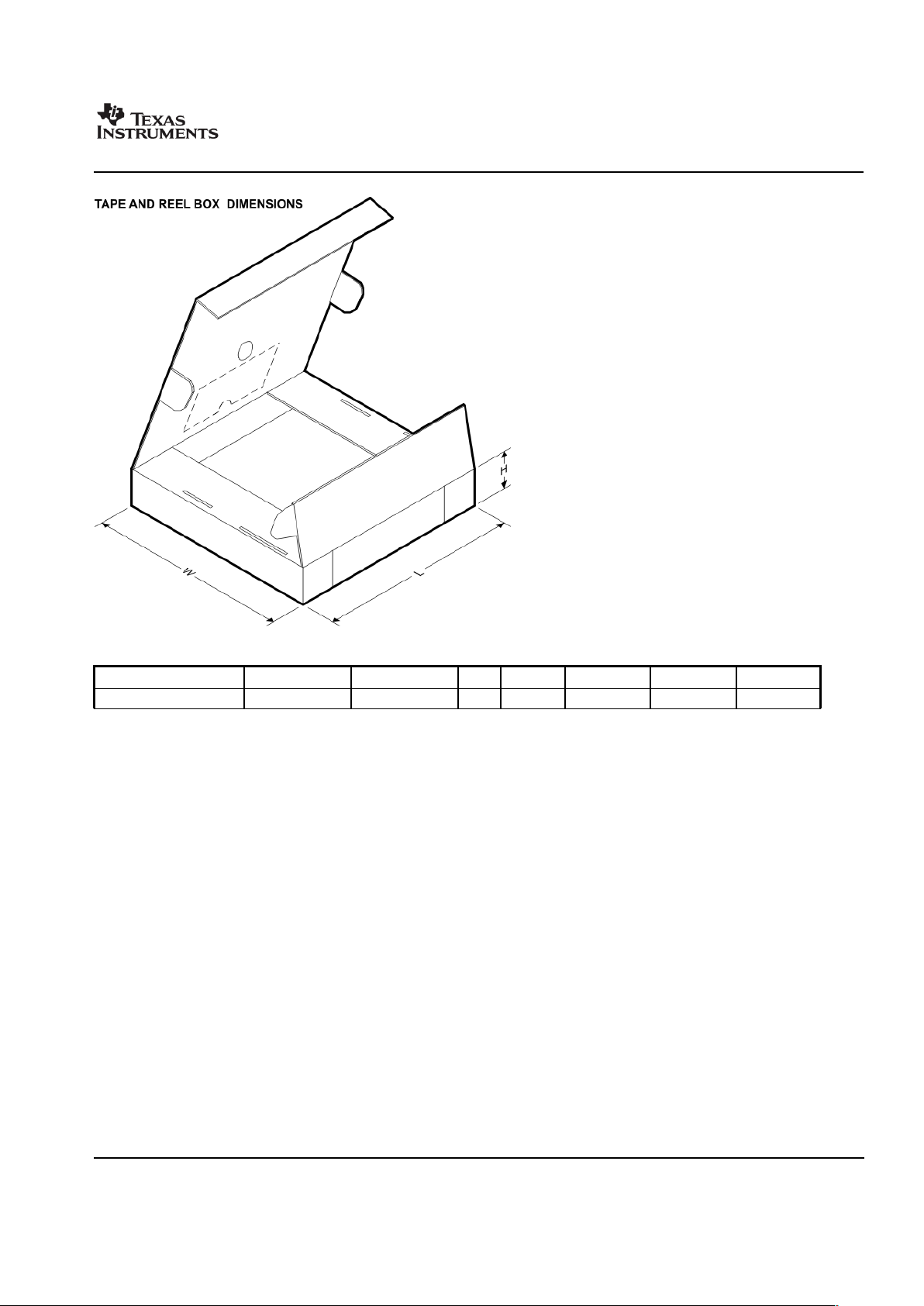
TAPE AND REEL INFORMATION
*All dimensions are nominal
Device Package
Type
Package
Drawing
Pins SPQ Reel
Diameter
(mm)
Reel
Width
W1 (mm)
A0 (mm) B0 (mm) K0 (mm) P1
(mm)W(mm)
Pin1
Quadrant
UCD7100PWPR HTSSOP PWP 14 2000 330.0 12.4 6.67 5.4 1.6 8.0 12.0 Q1
PACKAGE MATERIALS INFORMATION
www.ti.com
11-Mar-2008
Pack Materials-Page 1
Page 21
*All dimensions are nominal
Device Package Type Package Drawing Pins SPQ Length (mm) Width (mm) Height (mm)
UCD7100PWPR HTSSOP PWP 14 2000 346.0 346.0 29.0
PACKAGE MATERIALS INFORMATION
www.ti.com
11-Mar-2008
Pack Materials-Page 2
Page 22
Page 23
Page 24
Page 25
Page 26

IMPORTANT NOTICE
Texas Instruments Incorporated and its subsidiaries (TI) reserve the right to make corrections, modifications, enhancements, improvements,
and other changes to its products and services at any time and to discontinue any product or service without notice. Customers should
obtain the latest relevant information before placing orders and should verify that such information is current and complete. All products are
sold subject to TI’s terms and conditions of sale supplied at the time of order acknowledgment.
TI warrants performance of its hardware products to the specifications applicable at the time of sale in accordance with TI’s standard
warranty. Testing and other quality control techniques are used to the extent TI deems necessary to support this warranty. Except where
mandated by government requirements, testing of all parameters of each product is not necessarily performed.
TI assumes no liability for applications assistance or customer product design. Customers are responsible for their products and
applications using TI components. To minimize the risks associated with customer products and applications, customers should provide
adequate design and operating safeguards.
TI does not warrant or represent that any license, either express or implied, is granted under any TI patent right, copyright, mask work right,
or other TI intellectual property right relating to any combination, machine, or process in which TI products or services are used. Information
published by TI regarding third-party products or services does not constitute a license from TI to use such products or services or a
warranty or endorsement thereof. Use of such information may require a license from a third party under the patents or other intellectual
property of the third party, or a license from TI under the patents or other intellectual property of TI.
Reproduction of TI information in TI data books or data sheets is permissible only if reproduction is without alteration and is accompanied
by all associated warranties, conditions, limitations, and notices. Reproduction of this information with alteration is an unfair and deceptive
business practice. TI is not responsible or liable for such altered documentation. Information of third parties may be subject to additional
restrictions.
Resale of TI products or services with statements different from or beyond the parameters stated by TI for that product or service voids all
express and any implied warranties for the associated TI product or service and is an unfair and deceptive business practice. TI is not
responsible or liable for any such statements.
TI products are not authorized for use in safety-critical applications (such as life support) where a failure of the TI product would reasonably
be expected to cause severe personal injury or death, unless officers of the parties have executed an agreement specifically governing
such use. Buyers represent that they have all necessary expertise in the safety and regulatory ramifications of their applications, and
acknowledge and agree that they are solely responsible for all legal, regulatory and safety-related requirements concerning their products
and any use of TI products in such safety-critical applications, notwithstanding any applications-related information or support that may be
provided by TI. Further, Buyers must fully indemnify TI and its representatives against any damages arising out of the use of TI products in
such safety-critical applications.
TI products are neither designed nor intended for use in military/aerospace applications or environments unless the TI products are
specifically designated by TI as military-grade or "enhanced plastic." Only products designated by TI as military-grade meet military
specifications. Buyers acknowledge and agree that any such use of TI products which TI has not designated as military-grade is solely at
the Buyer's risk, and that they are solely responsible for compliance with all legal and regulatory requirements in connection with such use.
TI products are neither designed nor intended for use in automotive applications or environments unless the specific TI products are
designated by TI as compliant with ISO/TS 16949 requirements. Buyers acknowledge and agree that, if they use any non-designated
products in automotive applications, TI will not be responsible for any failure to meet such requirements.
Following are URLs where you can obtain information on other Texas Instruments products and application solutions:
Products Applications
Amplifiers amplifier.ti.com Audio www.ti.com/audio
Data Converters dataconverter.ti.com Automotive www.ti.com/automotive
DSP dsp.ti.com Broadband www.ti.com/broadband
Clocks and Timers www.ti.com/clocks Digital Control www.ti.com/digitalcontrol
Interface interface.ti.com Medical www.ti.com/medical
Logic logic.ti.com Military www.ti.com/military
Power Mgmt power.ti.com Optical Networking www.ti.com/opticalnetwork
Microcontrollers microcontroller.ti.com Security www.ti.com/security
RFID www.ti-rfid.com Telephony www.ti.com/telephony
RF/IF and ZigBee® Solutions www.ti.com/lprf Video & Imaging www.ti.com/video
Wireless www.ti.com/wireless
Mailing Address: Texas Instruments, Post Office Box 655303, Dallas, Texas 75265
Copyright © 2008, Texas Instruments Incorporated
 Loading...