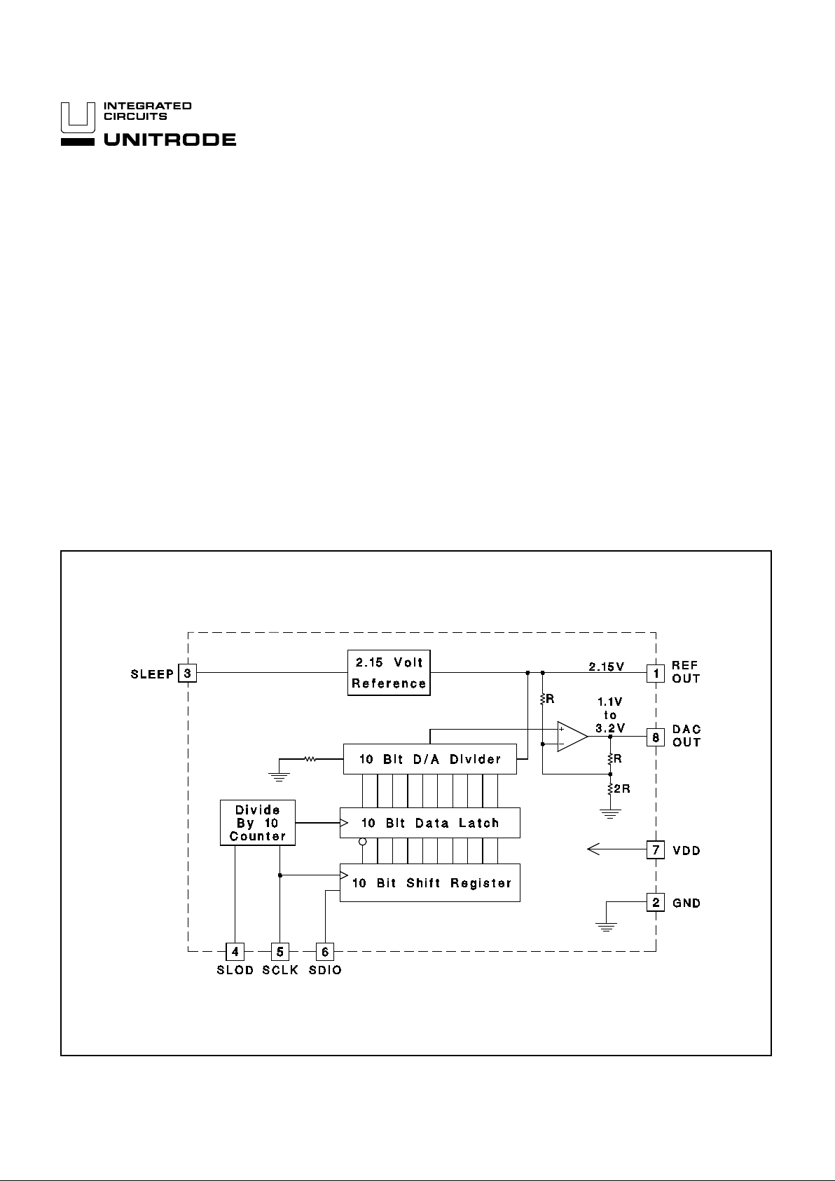
BLOCK DIAGRA M
2/95
FEATURES
• 10 Bit Resolution
• 1.1µs Output Rise Time
• 2.5µs Settling Time to 1%
• Single +5V Supply
• Monotonic
• Low Power Sleep Mode
• Three-wire Serial Interface
• 20MHz Data Rate
• 8 Pin SOIC and DIL Package
DESCRIPT IO N
The UCC5950 is a self-contained, microprocessor-compatible 10-bit D/A converter. It contains all of the functions required to take data directly from a threewire serial da ta bus and convert it to a preci se vol tage, i ncludi ng: an input shift
register, data latches, a p recisi on vo ltage reference, a precision 10-bit digital to
analog converter , and an output buffer amplifier.
The serial data interface i s cap able o f clo c k frequ enci es as hi gh as 20MHz, allowing update rates as high as two words per microsecond. The UCC5950 accepts commands encoded as 2’s-complement binary.
The data converter in the UCC5950 is inherently monotonic, making this part
ideal for use in closed-loop servo control systems as well as open-loop data
conversion. The UCC5950 uses a un ique segmented data converter which offers differential linea rity better than 1 LSB, integral linearity better than 2 LSB,
and fast conversion.
UCC5950
10-Bit Serial D/A Converter
UDG-95034

ABSOLUTE MAXIMUM RATINGS
VDD Supply Voltage. . . . . . . . . . . . . . . . . . . . . . . . . . . . . . . 6.5V
Input Voltage, Any I nput. . . . . . . . . . . . . . . . –0.3V to VDD+0.3V
Output Cur rent, Any Output . . . . . . . . . . . . . . . . . . . . . . . . ±5mA
Operating Tempe ratur e . . . . . . . . . . . . . . . . . . −55°C to +150°C
Stora g e Temperature. . . . . . . . . . . . . . . . . . . . −65°C to +150°C
Lead Temperature . . . . . . . . . . . . . . . . . . . . . . . . . . . . . . . 300°C
All voltages with respect to GND. All current s are positive int o,
negative out of, the sp ecifie d terminal. Consult Packa ging Section of Databook for thermal limitations and conside rations of
packages.
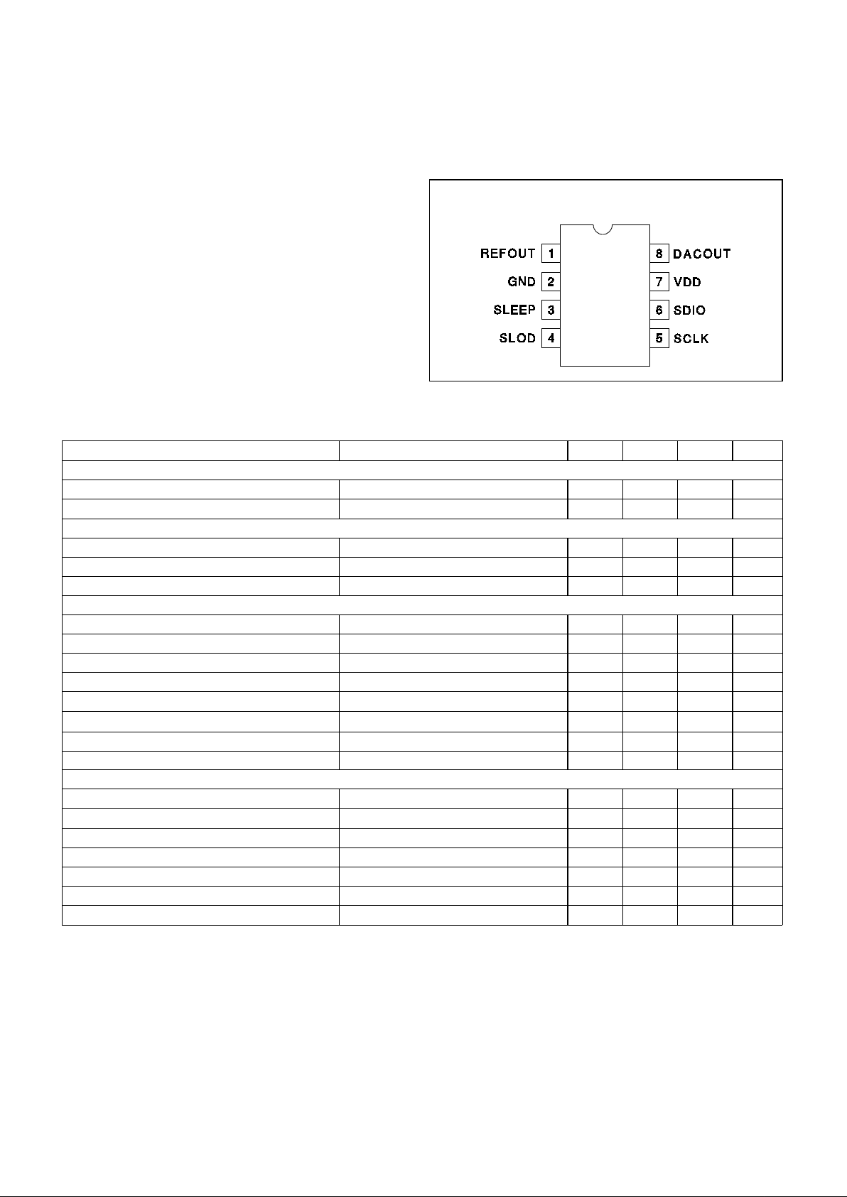
CONNECTION DIAG RAM
UCC5950
ELECTRICAL CHARACTERIST ICS Unless otherw ise stated, al l specificatio ns apply for 4.5V < VDD < 5.5V, REFOUT
Load < 100pF, DACOUT Load < 100pF, 0°C < T
A < +70°C, and TA = TJ.
PARAMETER TEST CONDITIONS MIN. TYP. MAX. UNITS
OVERALL SECTION
Supply Curren t SLEEP = 0V 1.5 5 mA
Supply Curren t SLEEP = 5V 0.1 10
µA
REFERENCE SECTION
REFOUT Output Volta ge 2.10 2.15 2.20 V
REFOUT Change with VDD 4.5V < VDD < 5.5V 1 10 mV
REFOUT Change with Load –1mA < I
REFOUT < 1mA 1 10 mV
D/A SECTION
Integral Nonlinearity (Note 1) 2 LSB
Differe ntial Nonlin earity 1 LSB
Full Scale Differe nce f ro m 1.49 24 x RE F –8 8 LSB
Zero Scale D ifference from 0.5089 x REF –8 8 LSB
DACOUT Full Scale Rise/Fall Time From 10% to 90% of swing (Note 4) 0.7 1.1
µs
DACOUT Full Scale Settling Time (TS) (Note 2, 3, 4) 1.4 2.5
µs
DACOUT Change with VDD 4.5V < VDD < 5.5V 1.5 10 mV
DACOUT Change with Load –1mA < I
DACOUT < 1mA 1.2 10 m V
LOGIC SECTION
Logic Input Thr esh old 1.5 2.5 3.5 V
Logic Input Cur ren t 0V < V
IN < VDD 5
µA
Logic Input Capacita nce (Note 4) 2.7 10 pF
SLOD Setup Time to SCLK low (TSLS) (Note 4) 50 ns
SLOD Hold Time from SCLK high (TSLH) From 10
TH
SCLK high (Note 4) 50 ns
SDIO Setup Time to SCLK high (TDS) (Note 4) 15 ns
SDIO Hold Time from SCLK high (TDH) (Note 4) 7 ns
Note 1: Integral nonlinear ity is defined as the worst deviat ion of the conve rter out put from th e best-fit straigh t line thro ugh
all converter ou tp ut codes.
Note 2: From 10
TH
Rising Edge of SCLK.
Note 3: Settling time is to 1% of final value.
Note 4: Guaranteed by design. Not 100% tested in production.
DIL-8, SOIC-8 (Top View)
N or J, D Package
2
 Loading...