Texas Instruments UCC3957MTR-3, UCC3957MTR-2, UCC3957MTR-1, UCC3957M-3, UCC3957M-2 Datasheet
...
UCC3957 -1/-2/-3/-4
PRELIMINARY
SLUS236 - JANUARY 1999
FEATURES
• Three or Four Cell Operation
• Two Tier Overcurrent Limiting
• 30µA Typical Supply Current
Consumption
• 3.5µA Typical Supply Current in Sleep
Mode
• Smart Discharge Minimizes Losses in
Overcharge Mode
• 6.5V to 20V VDD Supply Range
• Highly Accurate Internal Voltage
Reference
• Externally Adjustable Delays in
Overcurrent Controller
• Detection of Loss of Cell Sense
Connections
Three - Four Cell Lithium-Ion Protector Circuit
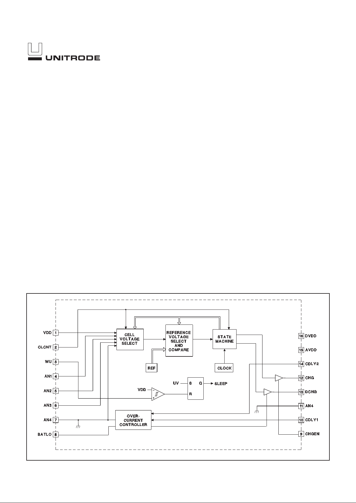
BLOCK DIAGRAM
UDG-97060
DESCRIPTION
The UCC3957 is a BiCMOS three or four cell lithium-ion battery pack
protector designed to operate with external P-channel MOSFETs. Utilizing external P-channel MOSFETs provides the benefits of no loss of
system ground in an overdischarge state, and protects the IC as well as
battery cells from damage during an overcharge state. An internal state
machine runs continuously to protect each lithium-ion cell from overcharge and overdischarge. A separate overcurrent protection block protects the battery pack from excessive discharge currents.
If any cell voltage exceeds the overvoltage threshold, the appropriate external P-channel MOSFET is turned off, preventing further charge current. An external N-channel MOSFET is required to level shift to this high
side P-channel MOSFET. Discharge current can still flow through the
second PFET. Likewise, if any cell voltage falls below the undervoltage
limit, the second P-channel MOSFET is turned off and only charge current is allowed. Such a cell voltage condition will cause the chip to go
into low power sleep mode. Attempting to charge the battery pack will
wake up the chip. A cell count pin (CLCNT) is provided to program the IC
for three or four cell operations.
A two tiered overcurrent controller and external current shunt protect the
battery pack from excessive discharge currents. If the first overcurrent
threshold level is exceeded, an internal timing circuit charges an external
capacitor to provide a user programmable blanking time.
(continued)

2
UCC3957 -1/-2/-3/-4
ELECTRICAL CHARACTERISTICS:
Unless otherwise specified, VDD = 16V and –20°C < TA< 70°C, TA= TJ.
All voltages measured with respect to the AN4 terminal.
PARAMETER TEST CONDITIONS MIN TYP MAX UNITS
Supply Section
Minimum V
DD
5.0 5.5 V
Supply Current 30 40 µA
Sleep Mode Supply Current VDD= 10.4V 3.5 7.5 µA
Output Section
DCHG Output Current Driving Logic Low and V
O
= 1V 40 70 100 µA
Driving Logic High and VO= VDD – 1 –20 –7 –3 mA
CHG Ouput Current Driving Logic Low and VO= 1V 40 70 100 µA
Driving Logic High and VO= VDD – 1V –20 –7 –3 mA
State Transitions
Normal to Overcharge UCC3957-1 4.15 4.20 4.25 V
Overcharge to Normal UCC3957-1 3.95 4.00 4.05 V
Normal to Overcharge UCC3957-2 4.20 4.25 4.30 V
Overcharge to Normal UCC3957-2 4.00 4.05 4.10 V
Normal to Overcharge UCC3957-3 4.25 4.30 4.35 V
Overcharge to Normal UCC3957-3 4.05 4.10 4.15 V
Normal to Overcharge UCC3957-4 4.30 4.35 4.40 V
Overcharge to Normal UCC3957-4 4.10 4.15 4.20 V
Undercharge to Normal 2.5 2.6 2.7 V
Normal to Undercharge 2.2 2.3 2.4 V
OV to CHG Delay (Note 1) 10 17 23 ms
ABSOLUTE MAXIMUM RATINGS
Supply Voltage . . . . . . . . . . . . . . . . . . . . . . . . . . . . . . . . . . 20V
Supply Current . . . . . . . . . . . . . . . . . . . . . . . . . . . . . . . . . 25mA
Output Current (CHG, DCHG) . . . . . . . . . . . . . . . . . . . . . 25mA
WU Input Voltage . . . . . . . . . . . . . . . . . . . . . . . . . . . . . . . . 28V
BATLO Input Voltage. . . . . . . . . . . . . . . . . . . . . . –0.3V to 2.5V
AN1 and AN3 Input Voltage . . . . . . . . . . . . . . . . . VAN4 – VDD
CLCNT and CHGEN. . . . . . . . . . . . . . . . . . . . . . . VAN4 – VDD
Storage Temperature . . . . . . . . . . . . . . . . . . . –65°C to +150°C
Junction Temperature. . . . . . . . . . . . . . . . . . . –55°C to +150°C
Lead Temperature (Soldering, 10 sec.). . . . . . . . . . . . . +300°C
Unless otherwise indicated, voltages are referenced to AN4.
Currents are positive into, negative out of the specified terminal.
Consult Packaging Section of Databook for thermal limitations
and considerations of packages.
DESCRIPTION (continued)
If at the end of the blanking time the overcurrent condition still exists, the external discharge FET is turned off
for a period 17 times longer than the first blanking period, and then the discharge FET is turned back on. If at
any time a second higher overcurrent threshold is ex-
ceeded for more than a user programmable time, the discharge FET is turned off, and will remain off for the same
period as the first tier off time. This two tiered overcurrent
protection scheme allows for charging capacitive loads
while retaining effective short circuit protection.
CDLY2
AVDD
DVDD
DCHG
CHG
CDLY1
AN4
CHGEN
1
2
3
4
5
6
7
8
16
15
14
13
12
11
10
9
CLCNT
VDD
BATLO
AN3
AN4
WU
AN1
AN2
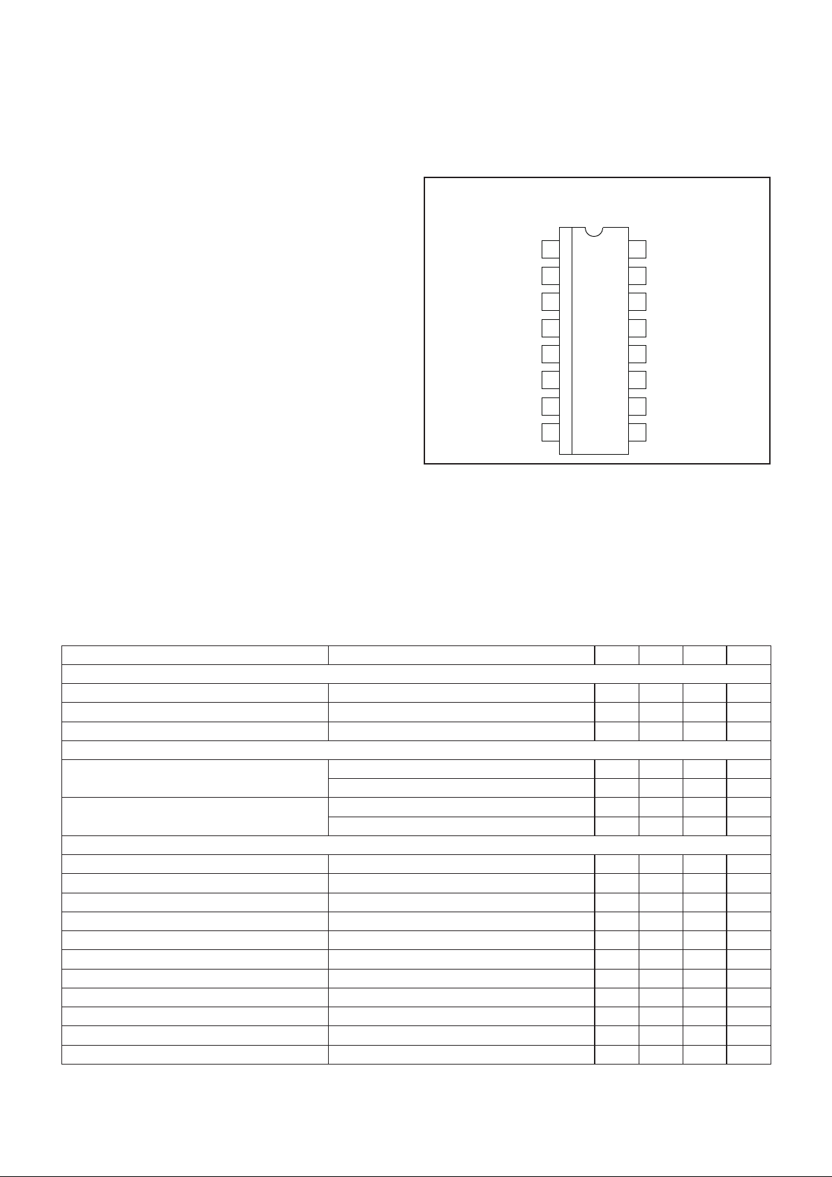
CONNECTION DIAGRAM
SSOP-16 (Top View)
M Package

3
UCC3957 -1/-2/-3/-4
PIN DESCRIPTIONS
AN1: Connects to the negative terminal of the top battery
cell and the positive terminal of the second battery cell.
AN2: Connects to the bottom terminal of the second
battery cell and the top terminal of the third battery cell.
AN3: Connects to the bottom terminal of the third battery
cell and the top terminal of the fourth battery cell in a four
cell stack. In a three cell pack it connects to the bottom
terminal of the third battery and to AN4.
AN4: Connects to the bottom terminal of the battery
stack and the top of the current sense resistor.
AVDD: Internal analog supply bypass cap pin. Connect a
0.1µF capacitor between this pin and AN4. This pin is
nominally 7.3V.
BATLO: Connects to the bottom of the current sense
resistor and the negative terminal of the battery pack.
CHGEN: The charge enable input for the protection IC.
This point must be driven high to allow charging of the
battery pack. This pin has a very weak pulldown.
CDLY1: Delay control pin for the short circuit protection
feature. A capacitor connected between this point and
AN4 will determine the time delay from when an
overcurrent situation is detected to when the FET is
turned off. This capacitor also controls the hiccup mode
timeout period.
CDLY2: An external cap can be tied between this pin
and AN4 to extend the blanking time on the second current limit tier.
CLCNT: This pin programs the IC for three or four cell
operation. Tying this pin low (to AN4) sets four cell operation, w`hile tying it high (to VDD or the preferred DSPLY
or ASPLY) sets three cell operation. This pin is internally
pulled low, so open circuit conditions will always result in
four cell mode.
DCHG: This pin is used to prevent overdischarge. If the
state machine indicates that any cell is undervoltage, this
pin will be driven high with respect to chip substrate so
that the external P-channel MOSFET will prevent further
discharge. If all cell voltages are above the minimum
threshold, this pin will be driven low.
CHG: This pin is used to control an external N-channel
MOSFET, which in turn drives a P-channel MOSFET. If at
least one cell voltage is over the OV threshold, this pin
will be driven low with respect to AN4. If all cell voltages
are below this threshold, this pin will be driven high.
DVDD: Internal digital supply bypass capacitor pin. Connect a 0.1µF capacitor between this pin and AN4. This
pin is nominally 7.3V.
VDD: Supply voltage to the IC. Connect this point to the
top of the lithium-ion battery stack.
WU: This pin is used to provide a wake up signal to the
IC during sleep mode. Connect this pin to the drain of the
N-channel level shift MOSFET.
ELECTRICAL CHARACTERISTICS: Unless otherwise specified, VDD = 16V and –20°C < T
A
< 70°C, TA= TJ.
All voltages measured with respect to the AN4 terminal.
PARAMETER TEST CONDITIONS MIN TYP MAX UNITS
State Transitions (continued)
UV to DCHG Delay (Note 1) 10 17 23 ms
Cell Sample Rate (Note 1) 5 8.5 11.5 ms
Smart Discharge Threshold BATLO Voltage 12 15 20 mV
Wakeup Input Threshold With Respect to V
DD 50 mV
Charge Enable Input Threshold 0.8 1.3 2.6 V
Short Circuit Protection
First Tier Threshold Level V
BATLO
120 150 180 mV
Second Tier Threshold Level V
BATLO
300 375 450 mV
First Tier Blanking Time CDLY1 = 0.1µF 305070ms
Restart Time CDLY1 = 0.1µF 300 500 700 ms
Second Tier Blanking Time CDLY2 = 10pF 200 400 550 µs
Note 1: Tested at probe only.
Note 2: Other OV/UV thresholds are available. Please consult the factory.
 Loading...