

Page 1

User’s Guide
July 2002 PMP Systems Power
SLLU049
Page 2

IMPORTANT NOTICE
Texas Instruments Incorporated and its subsidiaries (TI) reserve the right to make corrections, modifications,
enhancements, improvements, and other changes to its products and services at any time and to discontinue
any product or service without notice. Customers should obtain the latest relevant information before placing
orders and should verify that such information is current and complete. All products are sold subject to TI’s terms
and conditions of sale supplied at the time of order acknowledgment.
TI warrants performance of its hardware products to the specifications applicable at the time of sale in
accordance with TI’s standard warranty . Testing and other quality control techniques are used to the extent TI
deems necessary to support this warranty . Except where mandated by government requirements, testing of all
parameters of each product is not necessarily performed.
TI assumes no liability for applications assistance or customer product design. Customers are responsible for
their products and applications using TI components. T o minimize the risks associated with customer products
and applications, customers should provide adequate design and operating safeguards.
TI does not warrant or represent that any license, either express or implied, is granted under any TI patent right,
copyright, mask work right, or other TI intellectual property right relating to any combination, machine, or process
in which TI products or services are used. Information published by TI regarding third–party products or services
does not constitute a license from TI to use such products or services or a warranty or endorsement thereof.
Use of such information may require a license from a third party under the patents or other intellectual property
of the third party , or a license from TI under the patents or other intellectual property of TI.
Reproduction of information in TI data books or data sheets is permissible only if reproduction is without
alteration and is accompanied by all associated warranties, conditions, limitations, and notices. Reproduction
of this information with alteration is an unfair and deceptive business practice. TI is not responsible or liable for
such altered documentation.
Resale of TI products or services with statements different from or beyond the parameters stated by TI for that
product or service voids all express and any implied warranties for the associated TI product or service and
is an unfair and deceptive business practice. TI is not responsible or liable for any such statements.
Mailing Address:
Texas Instruments
Post Office Box 655303
Dallas, Texas 75265
Copyright 2002, Texas Instruments Incorporated
Page 3

EVM IMPORTANT NOTICE
Texas Instruments (TI) provides the enclosed product(s) under the following conditions:
This evaluation kit being sold by TI is intended for use for ENGINEERING DEVELOPMENT OR EV ALUA TION
PURPOSES ONL Y and is not considered by TI to be fit for commercial use. As such, the goods being provided
may not be complete in terms of required design-, marketing-, and/or manufacturing-related protective
considerations, including product safety measures typically found in the end product incorporating the goods.
As a prototype, this product does not fall within the scope of the European Union directive on electromagnetic
compatibility and therefore may not meet the technical requirements of the directive.
Should this evaluation kit not meet the specifications indicated in the EVM User’s Guide, the kit may be returned
within 30 days from the date of delivery for a full refund. THE FOREGOING WARRANTY IS THE EXCLUSIVE
WARRANTY MADE BY SELLER TO BUYER AND IS IN LIEU OF ALL OTHER WARRANTIES, EXPRESSED,
IMPLIED, OR ST ATUT ORY, INCLUDING ANY WARRANTY OF MERCHANTABILITY OR FITNESS FOR ANY
PARTICULAR PURPOSE.
The user assumes all responsibility and liability for proper and safe handling of the goods. Further, the user
indemnifies TI from all claims arising from the handling or use of the goods. Please be aware that the products
received may not be regulatory compliant or agency certified (FCC, UL, CE, etc.). Due to the open construction
of the product, it is the user’s responsibility to take any and all appropriate precautions with regard to electrostatic
discharge.
EXCEPT TO THE EXTENT OF THE INDEMNITY SET FORTH ABOVE, NEITHER P ARTY SHALL BE LIABLE
TO THE OTHER FOR ANY INDIRECT, SPECIAL, INCIDENTAL, OR CONSEQUENTIAL DAMAGES.
TI currently deals with a variety of customers for products, and therefore our arrangement with the user is not
exclusive.
TI assumes no liability for applications assistance, customer product design, software performance, or
infringement of patents or services described herein.
Please read the EVM User’s Guide and, specifically, the EVM Warnings and Restrictions notice in the EVM
User’s Guide prior to handling the product. This notice contains important safety information about temperatures
and voltages. For further safety concerns, please contact the TI application engineer.
Persons handling the product must have electronics training and observe good laboratory practice standards.
No license is granted under any patent right or other intellectual property right of TI covering or relating to any
machine, process, or combination in which such TI products or services might be or are used.
Mailing Address:
Texas Instruments
Post Office Box 655303
Dallas, Texas 75265
Copyright 2002, Texas Instruments Incorporated
Page 4

EVM WARNINGS AND RESTRICTIONS
It is important to operate this EVM within the input and output voltage ranges specified in the
user’s guide.
Exceeding the specified input range may cause unexpected operation and/or irreversible
damage to the EVM. If there are questions concerning the input range, please contact a TI
field representative prior to connecting the input power.
Applying loads outside of the specified output range may result in unintended operation and/or
possible permanent damage to the EVM. Please consult the EVM User’s Guide prior to
connecting any load to the EVM output. If there is uncertainty as to the load specification,
please contact a TI field representative.
During normal operation, some circuit components may have case temperatures greater than
60°C. The EVM is designed to operate properly with certain components above 60°C as long
as the input and output ranges are maintained. These components include but are not limited
to linear regulators, switching transistors, pass transistors, and current sense resistors. These
types of devices can be identified using the EVM schematic located in the EVM User’s Guide.
When placing measurement probes near these devices during operation, please be aware
that these devices may be very warm to the touch.
Mailing Address:
Texas Instruments
Post Office Box 655303
Dallas, Texas 75265
Copyright 2002, Texas Instruments Incorporated
Page 5

About This Manual
Related Documentation From Texas Instruments
Preface
Read This First
This users guide describes the characteristics, operation, and use of the
UCC2977 CCFL backlight converter evaluation module (EVM). The users
guide includes a schematic diagram, bill of materials and test results.
How to Use This Manual
This document contains the following chapters:
- Chapter 1—Hardware
- Chapter 2—Design Procedure
- Chapter 3—Test Results
Related Documentation From Texas Instruments
- Texas Instruments Users Manual, UCC3976/7 Users Manual, TI
Literature Number SLUU108
- Texas Instruments Data Sheet, UCC2977, TI Literature Number
SLUS499A
FCC Warning
This equipment is intended for use in a laboratory test environment only . It generates, uses, and can radiate radio frequency energy , and has not been tested
for compliance with the limits of computing devices pursuant to subpart J of
part 15 of FCC rules, which are designed to provide reasonable protection
against radio frequency interference. Operation of this equipment in other environments may cause interference with radio communications, in which case
the user at his own expense will be required to take whatever measures may
be required to correct this interference.
iii
Page 6

iv
Page 7

Contents
Contents
1 Hardware 1-1. . . . . . . . . . . . . . . . . . . . . . . . . . . . . . . . . . . . . . . . . . . . . . . . . . . . . . . . . . . . . . . . . . . . . . .
1.1 Introduction 1-2. . . . . . . . . . . . . . . . . . . . . . . . . . . . . . . . . . . . . . . . . . . . . . . . . . . . . . . . . . . . . . . .
1.2 Operating Specifications 1-2. . . . . . . . . . . . . . . . . . . . . . . . . . . . . . . . . . . . . . . . . . . . . . . . . . . . .
1.3 Schematic 1-3. . . . . . . . . . . . . . . . . . . . . . . . . . . . . . . . . . . . . . . . . . . . . . . . . . . . . . . . . . . . . . . . .
1.4 Bill of Materials 1-4. . . . . . . . . . . . . . . . . . . . . . . . . . . . . . . . . . . . . . . . . . . . . . . . . . . . . . . . . . . . .
1.5 Board Layout 1-5. . . . . . . . . . . . . . . . . . . . . . . . . . . . . . . . . . . . . . . . . . . . . . . . . . . . . . . . . . . . . .
2 Design Procedure 2-1. . . . . . . . . . . . . . . . . . . . . . . . . . . . . . . . . . . . . . . . . . . . . . . . . . . . . . . . . . . . . . .
2.1 Push-Pull Inductor Selection 2-2. . . . . . . . . . . . . . . . . . . . . . . . . . . . . . . . . . . . . . . . . . . . . . . . .
2.2 Frequency Range Setting 2-2. . . . . . . . . . . . . . . . . . . . . . . . . . . . . . . . . . . . . . . . . . . . . . . . . . . .
2.3 Analog Dimming of the Lamp 2-2. . . . . . . . . . . . . . . . . . . . . . . . . . . . . . . . . . . . . . . . . . . . . . . . .
2.4 Open-Lamp Voltage Programming 2-3. . . . . . . . . . . . . . . . . . . . . . . . . . . . . . . . . . . . . . . . . . . .
2.5 Shutdown 2-3. . . . . . . . . . . . . . . . . . . . . . . . . . . . . . . . . . . . . . . . . . . . . . . . . . . . . . . . . . . . . . . . . .
2.6 No Lock 2-3. . . . . . . . . . . . . . . . . . . . . . . . . . . . . . . . . . . . . . . . . . . . . . . . . . . . . . . . . . . . . . . . . . .
2.7 Burst Dimming 2-4. . . . . . . . . . . . . . . . . . . . . . . . . . . . . . . . . . . . . . . . . . . . . . . . . . . . . . . . . . . . .
2.8 Clamp Circuit (Optional) 2-4. . . . . . . . . . . . . . . . . . . . . . . . . . . . . . . . . . . . . . . . . . . . . . . . . . . . .
3 Test Results 3-1. . . . . . . . . . . . . . . . . . . . . . . . . . . . . . . . . . . . . . . . . . . . . . . . . . . . . . . . . . . . . . . . . . . . .
3.1 Test Setup 3-2. . . . . . . . . . . . . . . . . . . . . . . . . . . . . . . . . . . . . . . . . . . . . . . . . . . . . . . . . . . . . . . . .
3.1.1 Lighting CCFL 3-2. . . . . . . . . . . . . . . . . . . . . . . . . . . . . . . . . . . . . . . . . . . . . . . . . . . . . .
3.1.2 Analog Dimming Test 3-3. . . . . . . . . . . . . . . . . . . . . . . . . . . . . . . . . . . . . . . . . . . . . . . .
3.1.3 Burst Dimming Test 3-4. . . . . . . . . . . . . . . . . . . . . . . . . . . . . . . . . . . . . . . . . . . . . . . . . .
3.2 Test Results 3-5. . . . . . . . . . . . . . . . . . . . . . . . . . . . . . . . . . . . . . . . . . . . . . . . . . . . . . . . . . . . . . . .
v
Page 8

Contents
Figures
1–1 UCC2977EVM Schematic 1-3. . . . . . . . . . . . . . . . . . . . . . . . . . . . . . . . . . . . . . . . . . . . . . . . . . . . . .
1–2 Top Silk Screen With Top Copper Layer 1-5. . . . . . . . . . . . . . . . . . . . . . . . . . . . . . . . . . . . . . . . . .
1–3 Top Layer Copper 1-5. . . . . . . . . . . . . . . . . . . . . . . . . . . . . . . . . . . . . . . . . . . . . . . . . . . . . . . . . . . . .
1–4 Bottom Layer Copper 1-5. . . . . . . . . . . . . . . . . . . . . . . . . . . . . . . . . . . . . . . . . . . . . . . . . . . . . . . . . .
3–1 Test Setup 3-2. . . . . . . . . . . . . . . . . . . . . . . . . . . . . . . . . . . . . . . . . . . . . . . . . . . . . . . . . . . . . . . . . . .
3–2 Test Setup for Analog Dimming 3-3. . . . . . . . . . . . . . . . . . . . . . . . . . . . . . . . . . . . . . . . . . . . . . . . .
3–3 Test Setup for Burst Dimming 3-4. . . . . . . . . . . . . . . . . . . . . . . . . . . . . . . . . . . . . . . . . . . . . . . . . . .
3–4 Efficiency With a Low Profile Sumida Inductor 3-5. . . . . . . . . . . . . . . . . . . . . . . . . . . . . . . . . . . .
3–5 Efficiency With a High Profile Toko Inductor 3-5. . . . . . . . . . . . . . . . . . . . . . . . . . . . . . . . . . . . . . .
3–6 Transformer Input/Output Voltages at V
3–7 Transformer Input/Output Voltages at VI = 6 V 3-6. . . . . . . . . . . . . . . . . . . . . . . . . . . . . . . . . . . .
3–8 Burst Dimming With 50% Duty Cycle 3-6. . . . . . . . . . . . . . . . . . . . . . . . . . . . . . . . . . . . . . . . . . . .
3–9 Burst Dimming With 80% Duty Cycle 3-7. . . . . . . . . . . . . . . . . . . . . . . . . . . . . . . . . . . . . . . . . . . .
3–10 Open Lamp Protection 3-7. . . . . . . . . . . . . . . . . . . . . . . . . . . . . . . . . . . . . . . . . . . . . . . . . . . . . . . . .
= 3 V 3-6. . . . . . . . . . . . . . . . . . . . . . . . . . . . . . . . . . . .
I
Tables
1–1 Operating Specifications 1-2. . . . . . . . . . . . . . . . . . . . . . . . . . . . . . . . . . . . . . . . . . . . . . . . . . . . . . .
1–2 Bill of Materials Required for the UCC2977 (SLUP178) 1-4. . . . . . . . . . . . . . . . . . . . . . . . . . . . .
vi
Page 9

Chapter 1
Hardware
The UCC2977 evaluation module (SLUP178) provides a reference design for
evaluating the performance of a high efficiency CCFL backlight converter
using the UCC2977 (push-pull backlight controller). The device contains all of
the circuitry necessary to control a backlight converter. This chapter contains
the schematic, board layout, and the bill of materials. The evaluation module
(EVM) performance specifications are also given.
Topic Page
1.1 Introduction 1-2. . . . . . . . . . . . . . . . . . . . . . . . . . . . . . . . . . . . . . . . . . . . . . . . . .
1.2 Operating Specifications 1-2. . . . . . . . . . . . . . . . . . . . . . . . . . . . . . . . . . . . . .
1.3 Schematic 1-3. . . . . . . . . . . . . . . . . . . . . . . . . . . . . . . . . . . . . . . . . . . . . . . . . . . .
1.4 Bill of Materials 1-4. . . . . . . . . . . . . . . . . . . . . . . . . . . . . . . . . . . . . . . . . . . . . . .
1.5 Board Layout 1-5. . . . . . . . . . . . . . . . . . . . . . . . . . . . . . . . . . . . . . . . . . . . . . . . .
1-1
Page 10

Introduction
1.1 Introduction
The UCC2977 EVM (SLUP178) is a 1.8-W dc/ac inverter module used to drive
a cold cathode fluorescent lamp (CCFL) with a piezoelectric transformer
(PZT). This EVM consists of a push-pull circuit using the UCC2977 controller.
The principle of operation for the inverter is explained in the application section
of the UCC2977 data sheet.
1.2 Operating Specifications
This section summarizes the performance specifications of the SLUP178
converter. Table 1–1 lists the operating specifications for the SLUP178.
Table 1–1.Operating Specifications
Input voltage (VIN) 3~6 Vdc
Output voltage (Lamp_HV, Lamp LV) 300 V ac, rms
Output current (lamp current) 4.7 mA, rms
Operating frequency (kHz) 100 kHz
Burst dimming (BD )
Analog dimming (AD) 0~3 Vdc
CCFL lamp JKL BF3100–20B (100 mm, 270 V
†
Use a function generator.
†
Square wave, 120 Hz, 0 to 3 V
RMS
)
1-2
Page 11
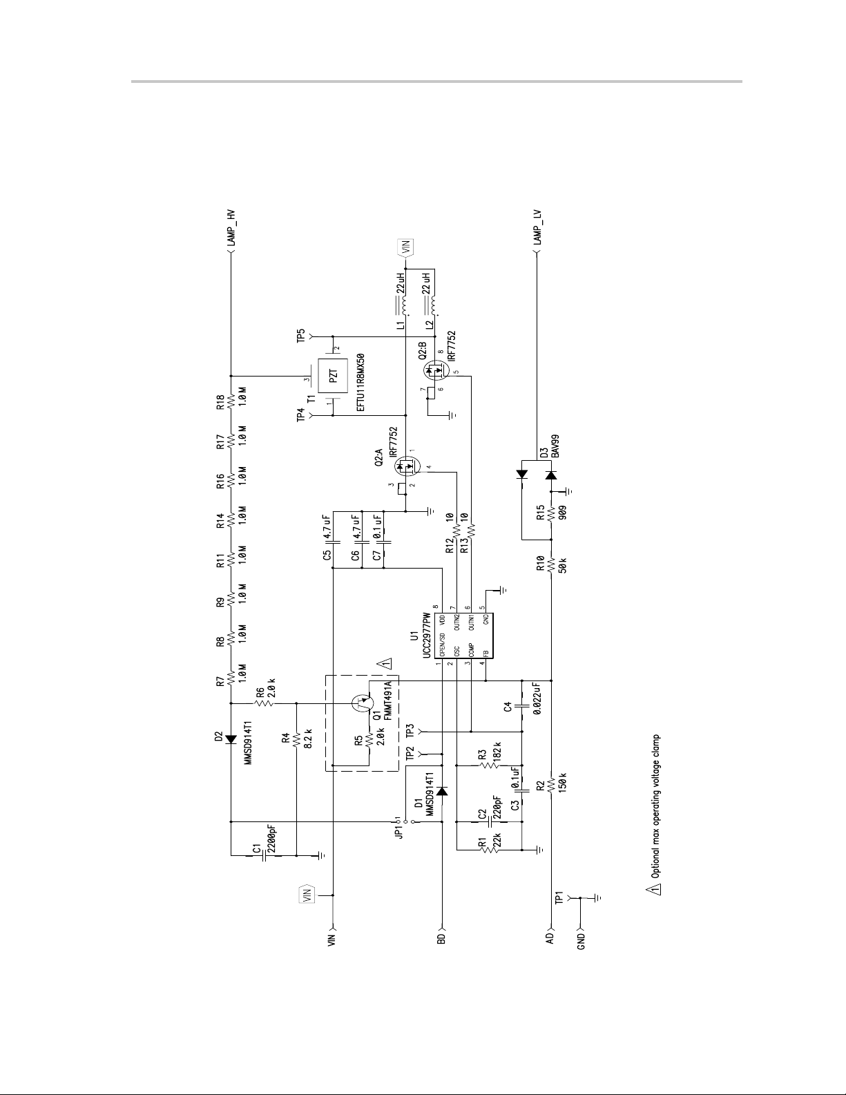
1.3 Schematic
Figure 1–1.UCC2977EVM Schematic
Schematic
Hardware
1-3
Page 12

Bill of Materials
1.4 Bill of Materials
Table 1–2.Bill of Materials Required for the UCC2977 (SLUP178)
Count Ref Des Description Size MFR Part Number
1 C1 Capacitor, ceramic, 2200 pF , 50 V ,
1 C2 Capacitor, ceramic, 220 pF, 50 V,
2 C3, C7 Capacitor, ceramic, 0.1 µF, 25 V,
1 C4 Capacitor, ceramic, 0.022 µF,
2 C5, C6 Capacitor, ceramic, 4.7 µF, 10 V,
2 D1, D2 Diode, switching, 1.0 mA, 75 V SOD123 Motorola MMSD914T1
1 D3 Diode, dual ultra fast, series,
1 JP1 Header, 3 pin, 100 mil spacing,
2 L1, L2 Inductor, SMT, 22 µH, 1.2 A,
1 Q1 Transistor, NPN, high perfor-
1 Q2 XSTR, MOSFET, N-channel,
1 R1 Resistor, chip, 22 kΩ, 1/16 W , 1% 603 Std Std
1 R10 Resistor, chip, 50 kΩ, 1/16 W, 1% 603 Std Std
2 R12, R13 Resistor, chip, 10 Ω, 1/16 W , 1% 603 Std Std
1 R15 Resistor, chip, 909 Ω, 1/16 W , 1% 603 Std Std
1 R2 Resistor, chip, 150 kΩ, 1/16 W , 1% 603 Std Std
1 R3 Resistor, chip, 182 kΩ, 1/16 W , 1% 603 Std Std
1 R4 Resistor, chip, 8.2 kΩ, 1/16 W , 1% 603 Std Std
2 R5, R6 Resistor, chip, 2.0 kΩ, 1/16 W, 1% 603 Std Std
8 R7, R8. R9.
R11, R14,
R16, R17,
R18
1 T1 Transformer , custom,
2 TP1, GND Test point, black, 1 mm 0.038 Farnell 240-333
9 TP2–TP5,
VIN, BD, AD,
LAMP_HV,
LAMP_LV
1 U1 IC, CCFL push-pull driver TSSOP-08 TI UCC2977PW
1 — PCB, 3.55I × 0.905I × 0.62I Any SLUP178
X7R, 20%
X7R, 20%
X7R, 20%
25 V , X7R, 20%
X5R, 20%
200 mA, 70 V
(36-pin strip)
128 mΩ
(or Toko inductor, 22 µH, 115 mΩ 7.6 × 7.6 × 5.1 mm Toko 646CY-220M
mance, 500 mA
30 V, 4.6 A, Rds 35 mΩ
Resistor, chip, 1.0 MΩ, 1/10 W,1%805 Std Std
Piezoelectric, SMT
Test point, red, 1 mm 0.038 Farnell 240-345
603 Murata GRM188R71H222KA01
603 Murata GRM188R7H221KD01
805 Murata GRM21BR71E104KA01
603 Murata GRM188R71E223KA01
1206 Murata GRM31CR61A475KA01
SOT23 Fairchild BAV99
0.100 × 3I Sullins PTC36SAAN
6.7 × 6.7 × 3 mm Sumida CDRH6D28-220NC
SOT23 ZeTek FMMT491A
TSSOP8 IR IRF7752
0.760 × 0.244 Panasonic EFTU11R8MX50
1-4
Page 13

1.5 Board Layout
Figure 1–2.Top Silk Screen With Top Copper Layer
Figure 1–3.Top Layer Copper
Board Layout
Figure 1–4.Bottom Layer Copper
Hardware
1-5
Page 14

1-6
Page 15

Chapter 2
Design Procedure
This chapter describes how to design the UCC2977EVM.
Topic Page
2.1 Push-Pull Inductor Selection 2-2. . . . . . . . . . . . . . . . . . . . . . . . . . . . . . . . . . .
2.2 Frequency Range Setting 2-2. . . . . . . . . . . . . . . . . . . . . . . . . . . . . . . . . . . . . .
2.3 Analog Dimming of the Lamp 2-2. . . . . . . . . . . . . . . . . . . . . . . . . . . . . . . . . .
2.4 Open-Lamp V oltage Programming 2-3. . . . . . . . . . . . . . . . . . . . . . . . . . . . . .
2.5 Shutdown 2-3. . . . . . . . . . . . . . . . . . . . . . . . . . . . . . . . . . . . . . . . . . . . . . . . . . . .
2.6 No Lock 2-3. . . . . . . . . . . . . . . . . . . . . . . . . . . . . . . . . . . . . . . . . . . . . . . . . . . . . .
2.7 Burst Dimming 2-4. . . . . . . . . . . . . . . . . . . . . . . . . . . . . . . . . . . . . . . . . . . . . . .
2.8 Clamp Circuit (Optional) 2-4. . . . . . . . . . . . . . . . . . . . . . . . . . . . . . . . . . . . . . .
Design Procedure
2-1
Page 16

Push-Pull Inductor Selection
Ȳ
ȴ
2.1 Push-Pull Inductor Selection
The push-pull topology requires a different approach for calculating the
external inductor values. Referring to Figure 1–1, Q2A and Q2B are driven out
of phase at 50% duty cycle. When Q2A is on, current is ramped up in L1.
During the next switch cycle Q2B is turned on, Q2A is turned off, and the
energy stored in L1 is transferred through the piezoelectric transformer. L1
resonates with the piezoelectric primary capacitance forming a half sinusoid
at Q2A’s drain. In order to achieve zero-voltage switching, the drain voltage
must return to ground before the next switching cycle. This dictates that the
LC resonant frequency must be greater than the switching frequency.
L t
In the EVM with a 100 kHz switching frequency and 61.6 nF piezoelectric
transformer, L1 and L2 must be less than 41 µH for zero-voltage switching, so
22-µH inductors are used.
A suitable capacitor must be chosen so that the peak-to-peak output ripple is
within the limits allowable for the application.
4 p
2
2.2 Frequency Range Setting
The VCO frequency range is programmed with external components R1, R3
and C2. The frequency is determined by the voltage decay from 1.7 V to 0.6 V
at the OSC pin. When the voltage reaches 0.6 V, an internal current source
charges OSC back to 1.7 V . The decay time is determined by the value of C2
and the discharge currents generated in R1 and R3. An accurate NPO
capacitor is recommended for C2 and 1% resistors are recommended for R1
and R3. The output frequency range can be calculated by equation 2:
COMP
Ǔ
+
ƒǒV
1
ƒ2 Cp
2 ln
R1 ) R3
ƪ
R1 R3 C2
ȱ
1.7 V (R1 ) R3) * V
ȧ
ǒ
0.6 V * V
COMP
ƫ
R1
COMP
Ǔ
R1 ) 0.6 V R3
(1)
(2)
ȳ
ȧ
With C2 set at 220 pF , R1 at 22 kΩ and R3 at 182 kΩ, the frequency is 100 kHz.
2.3 Analog Dimming of the Lamp
For analog dimming, enable the open-lamp detection by connecting pin 1 to
pin 2 of jumper JP1 and ground BD. Lamp intensity is controlled with the signal
AD.
The RMS lamp current becomes:
ƪ
1.5 V (R2 ) R10) * VAD R10
+
2-2
I
LAMP
Ǹ
2
R2 R15
ƫ
p
(3)
Page 17

Open-Lamp Voltage Programming
Zero volts on VAD commands full current while 3 V commands minimum
current. For the initially configured EVM, maximum current is 4.8 mA. R15 is
selected to be 909 Ω setting V
set to 150 K, R10 is calculated to be 50 K. The control-voltage to lamp-current
equation for the EVM is:
to 0 V and lamp current to 4.8 mA. With R2
AD
I
(mA) + 4.89 * 1.22 V
LAMP
2.4 Open-Lamp Voltage Programming
It is necessary to suspend the power-stage operation if an open lamp occurs
because the piezoelectric transformer has a high gain. The open-lamp
detection circuit is composed of voltage divider R7, R8, R9, R11, R14, R16,
R17, R18, R4, R6, D2, and C1. A 1.5 V comparator at the OPEN pin shuts
down the inverter if an open lamp is triggered. The RMS secondary voltage at
which an open lamp shutdown occurs can be calculated by equation (5).
9
V
OPEN
ǒ
1.5 V ) V
+
With R7~R9, R11, R14, R16~R18 at 1 Meg each, R6 at 2 k and R4 at 8.2 k,
the RMS value of open lamp threshold voltage at the secondary is 1220 V
The value of capacitor C1 should be large enough to filter the sinusoid
waveform into dc. For this board, 2200 pF was chosen. If C5 is too large, it
takes extra time for OPEN/SD to climb to 1.5 V when the output voltage hits
the open-lamp threshold, resulting in a higher output voltage than the set
value.
diode
Ǔ
ǒ
R
S
) R11) R14) S
i
i+7
2Ǹ (R4 ) R6)
AD
18
j+16
R
) R4) R6
j
Ǔ
RMS
(4)
(5)
RMS
.
2.5 Shutdown
2.6 No Lock
The open-lamp level should be set high enough to avoid tripping during normal
operation. Open-lamp detection is disabled for the burst-dimming mode by
connecting pin 3 to pin 2 of JP1. Connect pin 1 to pin 2 of JP1 to enable open
lamp protection.
The OPEN/SD pin is used for both open-lamp detection and commanded
shutdown. When a voltage higher than 2.5 V is applied to OPEN/SD through
D1, the part enters the shutdown or sleep mode where the oscillator is inactive
and both outputs are high. In this mode, the part draws little current at the V
pin and the OPEN/SD pin.
If the part fails to achieve regulation before reaching minimum frequency
(comp >2.2 V), it causes an internal retry counter to increment and then
attempt another start up. If the application does not operate normally after 7
attempts, the controller enters an error-induced shutdown state removing
power to the load.
Design Procedure
DD
2-3
Page 18

Burst Dimming
2.7 Burst Dimming
Burst dimming can be implemented at the OPEN/SD pin at the cost of
open-lamp detection.
Connect pin 2 to pin 3 of JP1 to disable the open-lamp detection circuit during
burst dimming mode.
Since the feedback loop does not need to operate with minimum lamp current
(as with analog dimming), the feedback capacitor, C4, can be reduced to 22
nF to improve the response time when the lamp restrikes.
To implement burst dimming on the EVM, AD should be grounded to set
maximum lamp brightness. A low-frequency 0 V – 4 V square wave applied
to BD will modulate the lamp current between zero and full intensity at the
desired frequency. A low-frequency repetition rate greater than 120 Hz is
recommended to avoid visible flicker. Applying 5 V at BD forces the lamp
current to zero, where 0 V at BD will force maximum lamp current. The duty
cycle of the square wave determines the lamp brightness as a percent of rated
lamp current.
2.8 Clamp Circuit (Optional)
V
CLAMP
There is also a clamp circuit to limit the maximum secondary voltage.
This circuit is typically not needed since the CCFL strikes or the open-lamp
circuit triggers before destructive levels are reached.
If R5 and Q1 are added to the board, the peak clamp voltage for the EVM is
given by equation (6):
Since the feedback loop does not need to operate with minimum lamp current
(as with analog dimming), the feedback capacitor, C4, can be reduced to 22
nF to improve the response time when the lamp restrikes.
(
ǒ
+
1.5 V) V
The peak clamped voltage for the evaluation board is 2200V.
The evaluation board components can be modified depending on the
application requirements. A supply between 3 Vdc and 6 Vdc is required for
this board to operate a 270~450 V cold-cathode fluorescent lamp (CCFL) from
1 mA to 4.8 mA. The input voltage range changes with different voltage lamp.
be
R7)R8)R9)R11)R14)R16)R17)R18)R6)R4
Ǔ
R4
)
PEAK
(6)
2-4
Page 19

Chapter 3
Test Results
This chapter describes how to properly connect and setup the UCC2977EVM.
It also presents the test results, which cover efficiency, burst dimming, and
open-lamp protection.
Topic Page
3.1 Test Setup 3-2. . . . . . . . . . . . . . . . . . . . . . . . . . . . . . . . . . . . . . . . . . . . . . . . . . . .
3.2 T est Results 3-5. . . . . . . . . . . . . . . . . . . . . . . . . . . . . . . . . . . . . . . . . . . . . . . . . .
Test Results
3-1
Page 20

Test Setup
3.1 Test Setup
3.1.1 Lighting CCFL
Figure 3–1.Test Setup
Power Supply
A power supply with a power capability of 6 V/0.5 A is required for this test.
Figure 3–1 shows the input/output connections to the SLUP178. Connect a
270-V lamp (BF3100–20B). Connect pin 1 to pin 2 of jumper JP1.
CCFL
Lamp
3-2
Page 21

3.1.2 Analog Dimming Test
For analog dimming, enable the open-lamp detection by connecting pin 1 to
pin 2 of jumper JP1. A power supply that has a power capability of 6 V/0.5 A
is required for this test. Figure 3–2 shows the input/output connections to the
SLUP178. The lamp intensity is controlled by V
wire of the lamp is as short as possible and the lamp reflector (if there is one)
is grounded to board ground. Do not let the high voltage wire cross any part
of the board.
Figure 3–2.Test Setup for Analog Dimming
Power Supply
Test Setup
(0~3 Vdc). Make sure the
AD
Power Supply
CCFL
Lamp
Test Results
3-3
Page 22

Test Setup
3.1.3 Burst Dimming Test
Connect pin 2 to pin 3 of JP1 to disable the open-lamp detection circuit during
burst dimming. A low frequency ( >100 Hz) 0~4 V square wave applied to BD
modulates the lamp current.
Figure 3–3.Test Setup for Burst Dimming
Power Supply
CCFL
Lamp
Function
Generator
+ –
3-4
Page 23

Test Results
3.2 Test Results
The test results for the SLUP178 are shown in this section.
Figure 3–4.Efficiency With a Low Profile Sumida Inductor (CDRH6D28; 22 µH, 128 mΩ,
6.7 × 6.7 × 3 mm)
EFFICIENCY
vs
90
85
80
75
70
65
Efficiency – %
60
55
50
3456
INPUT VOLTAGE
4.7 mA
4 mA
3 mA
2 mA
VI – Input Voltage – V
Figure 3–5.Efficiency With a High Profile Toko Inductor (646CY–220M; 22 µH,
115 mΩ, 7.6 × 7.6 × 5.1 mm)
EFFICIENCY
vs
90
85
80
75
70
65
Efficiency – %
60
55
50
3456
INPUT VOLTAGE
4.8 mA
2 mA
3 mA
VI – Input Voltage – V
4 mA
Test Results
3-5
Page 24

Test Results
Figure 3–6.Transformer Input/Output Voltages at VI = 3 V (CH1=Primary 1,
CH4=Primary 2, M1=Transformer Primary Voltage, CH3=Lamp Voltage)
Figure 3–7.Transformer Input/Output Voltages at VI = 6 V (CH1=Primary 1,
CH4=Primary 2, M1=Transformer Primary Voltage, CH3=Lamp Voltage)
Figure 3–8.Burst Dimming With 50% Duty Cycle (CH1=Burst Dimming Control Signal,
CH3=Lamp Voltage)
3-6
Page 25

Test Results
Figure 3–9.Burst Dimming With 80% Duty Cycle (CH1=Burst Dimming Control Signal,
CH3=Lamp Voltage)
Figure 3–10. Open Lamp Protection (CH1=Comp, C2=Open/SD)
Test Results
3-7
Page 26

3-8
 Loading...