

UCC1946
UCC2946
UCC3946
SLUS247B - FEBRUARY 2000
FEATURES
•
Fully Programmable Reset Threshold
•
Fully Programmable Reset Period
•
Fully Programmable Watchdog Period
•
2% Accurate Reset Threshold
•
VDD Can Go as Low as 2V
•
18µA Maximum IDD
•
Reset Valid Down to 1V
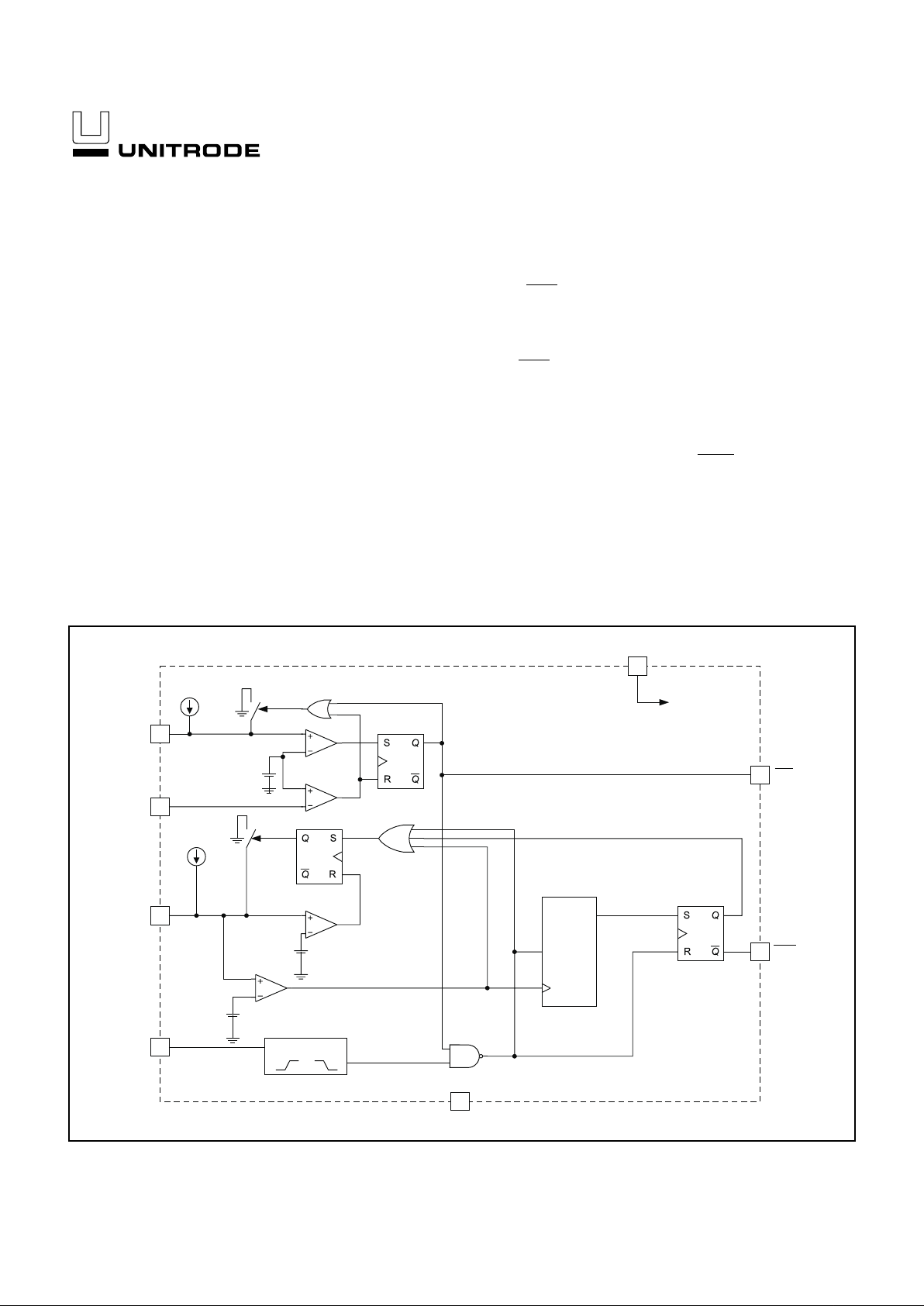
Microprocessor Supervisor with Watchdog Timer
6
7WDI
WP
8
VDD
3RES
5
POWER TO
CIRCUITRY
A3
A2
A1
A0
CLK
CLR
8-BIT COUNTER
400nA
WDO
1
GND
EDGE DETECT
WATCHDOG TIMING
100mV
1.235V
2RTH
4RP
1.235V .
400nA
POWER ON RESET
BLOCK DIAGRAM
Note: Pinout represents the 8-pin TSSOP package.
UDG-98001
DESCRIPTION
The UCC3946 is designed to provide accurate microprocessor supervi
sion, including reset and watchdog functions. During power up, the IC
asserts a reset signal RES
with VDD as low as 1V. The reset signal re
mains asserted until the VDD voltage rises and remains above the re
set threshold for the reset period. Both reset threshold and reset period
are programmable by the user. The IC is also resistant to glitches on
the VDD line. Once RES
has been deasserted, any drops below the
threshold voltage need to be of certain time duration and voltage mag
nitude to generate a reset signal. These values are shown in Figure 1.
An I/O line of the microprocessor may be tied to the watchdog input
(WDI) for watchdog functions. If the I/O line is not toggled within a set
watchdog period, programmable by the user, WDO
will be asserted.
The watchdog function will be disabled during reset conditions.
The UCC3946 is available in 8-pin SOIC(D), 8-pin DIP (N or J) and
8-pin TSSOP(PW) packages to optimize board space.
2
UCC1946
UCC2946
UCC3946
ELECTRICAL CHARACTERISTICS:
Unless otherwise specified, VDD = 2.1V to 5.5V for UCC1946 and UCC2946;
VDD = 2V to 5.5V for UCC3946; TA = 0°C to 70°C for UCC3946, –40°C to 95°C for UCC2946, and –55°C to 125°C for UCC1946;
T
A =TJ
PARAMETERS TEST CONDITIONS MIN TYP MAX MIN TYP MAX UNITS
UCC3946 UCC1946 & UCC2946
Operating Voltage 2.0 5.5 2.1 5.5 V
Supply Current 10 18 12 18 µA
Minimum VDD (Note 1) 1 1.1 V
Reset Section
Reset Threshold VDD Rising 1.210 1.235 1.260 1.170 1.235 1.260 V
Threshold Hysteresis 15 15 mV
Input Leakage 55nA
Output High Voltage I
SOURCE = 2mA VDD –
0.3
VDD –
0.3
V
Output Low Voltage I
SINK = 2mA 0.1 0.1 V
VDD = 1V, I
SINK = 20uA 0.2 0.4 V
VDD to Output Delay VDD = -1mV/µs (Note 2) 120 120 µs
Reset Period C
RP = 64nF 160 200 260 140 200 320 ms
Watchdog Section
WDI Input High 0.7·
V
DD
0.7·
V
DD
V
WDI Input Low 0.3·
VDD
0.3·
V
DD
V
Watchdog Period C
WP = 64nF 1.12 1.60 2.08 0.96 1.60 2.56 s
Watchdog Pulse Width 50 50 ns
Output High Voltage I
SOURCE = 2mA VDD –
0.3
VDD –
0.3
V
Output Low Voltage I
SINK = 2mA 0.1 0.1 V
Note 1: This is the minimum supply voltage where RES is considered valid.
Note 2: Guaranteed by design.Not 100% tested in production.
ABSOLUTE MAXIMUM RATINGS
VIN . . . . . . . . . . . . . . . . . . . . . . . . . . . . . . . . . . . . . . . . . . . . 10V
Storage Temperature . . . . . . . . . . . . . . . . . . . –65°C to +150°C
Junction Temperature. . . . . . . . . . . . . . . . . . . –55°C to +150°C
Lead Temperature (Soldering, 10 sec.). . . . . . . . . . . . . +300°C
Currents are positive into, negative out of the specified terminal.
Consult Packaging Section of the Databook for thermal limita
-
tions and considerations of packages.
WP
WDI
VDD
WDO
1
2
3
4
8
7
6
5
RTH
GND
RES
RP
SOIC-8, TSSOP-8, DIL-8 (Top View)
D, PW, N or J Package
CONNECTION DIAGRAM
3
UCC1946
UCC2946
UCC3946
The UCC3946 supervisory circuit provides accurate re
-
set and watchdog functions for a variety of microproces
sor applications. The reset circuit prevents the
microprocessor from executing code during undervoltage
conditions, typically during power-up and power-down. In
order to prevent erratic operation in the presence of
noise, voltage “glitches” whose voltage amplitude and
time duration are less than the values specified in Fig. 1
are ignored.
The watchdog circuit monitors the microprocessor’s activity, if the microprocessor does not toggle WDI during
the programmable watchdog period WDO
will go low,
alerting the microprocessor’s interrupt of a fault. The
WDO
pin is typically connected to the non-maskable in
-
put of the microprocessor so that an error recovery rou
-
tine can be executed.
APPLICATION INFORMATION
0
20
40
60
80
100
120
140
160
180
200
100 110 120 130 140 150 160 170 180
DELAY (µS)
OVERDRIVE VOLTAGEWITH
RESPECT TORESET THRESHOLD (mV)
RT SENSES GLITCH,
RES GOES LOW FOR RESET PERIOD
GLITCHES ARE IGNORED,
RESB REMAINS HIGH
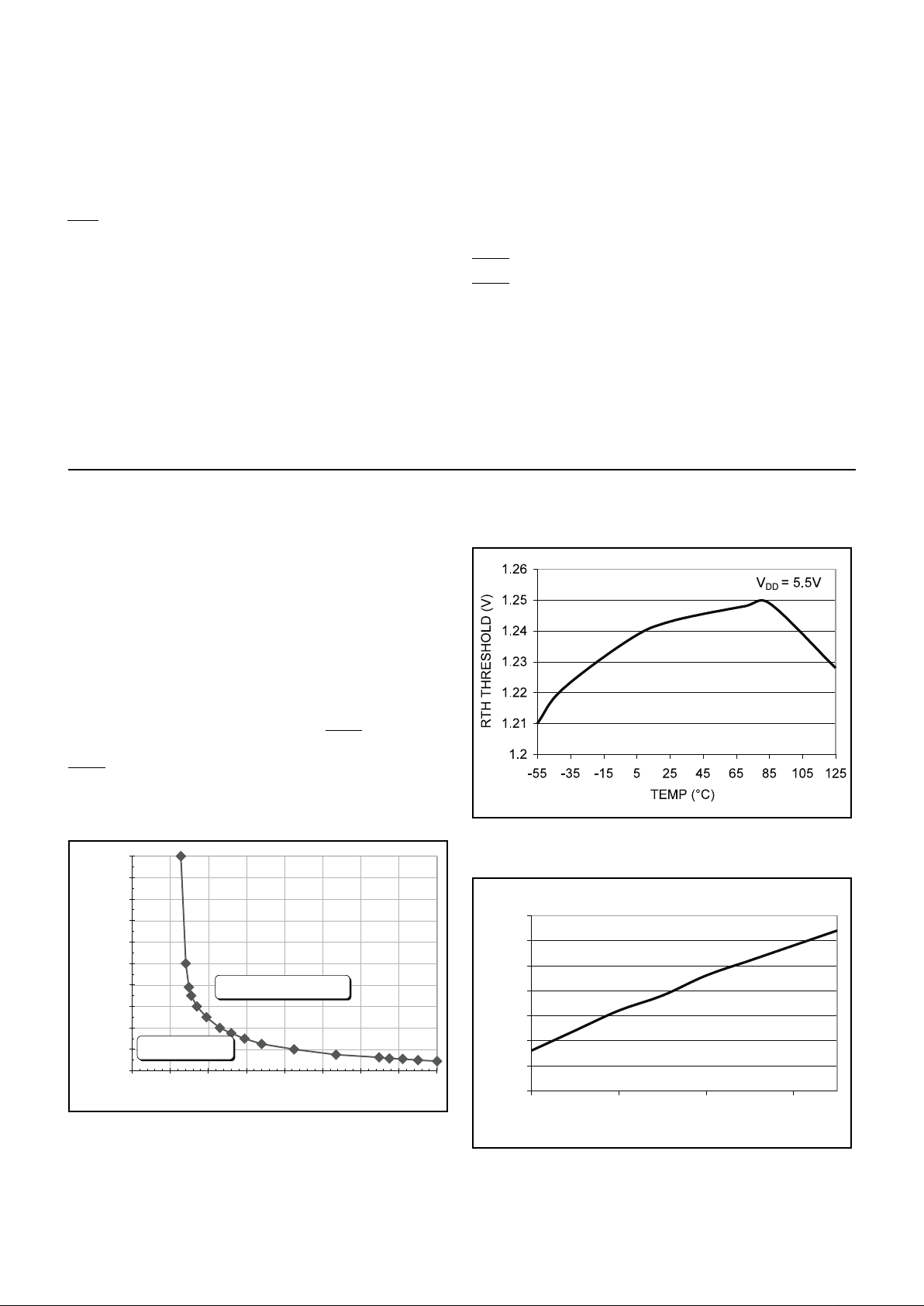
Figure 1. Overdrive voltage vs. delay to output low
on RESB.
Slew rate:–1V/mS;monitored voltage = VDD.
GND: Ground reference for the IC.
RES
: This pin is high only if the voltage on the RTH has
risen above 1.235V.Once RTH rises above the threshold,
this pin remains low for the reset period. This pin will also
go low and remain low if the RTH voltage dips below
1.235V for an amount of time determined by Figure 1.
RTH: This input compares its voltage to an internal 1.25V
reference. By using external resistors, a user can pro
-
gram any reset threshold he wishes to achieve.
RP: This pin allows the user to program the reset period
by adjusting an external capacitor.
VDD: Supply voltage for the IC.
WDI: This pin is the input to the watchdog timer. If this
pin is not toggled or strobed within the watchdog period,
WDO
is asserted.
WDO
: This pin is the watchdog output. This pin will be
asserted low if the WDI pin is not strobed or toggled
within the watchdog period.
WP: This pin allows the user to program the watchdog
period by adjusting an external capacitor.
PIN DESCRIPTIONS
Figure 2. Typical RTH threshold vs. temperature.
9
9.5
10
10.5
11
11.5
12
12.5
2345
VDD (V)
IDD (uA)
Figure 3. Typical IDD vs VDD.
4
UCC1946
UCC2946
UCC3946
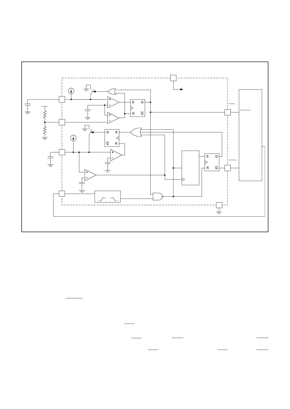
Programming the Reset Voltage and Reset Period
The UCC3946 allows the reset trip voltage to be pro
grammed with two external resistors.In most applications
VDD is monitored by the reset circuit, however, the de
sign allows voltages other than VDD to be monitored.
Referring to Fig. 4, the voltage below which reset will be
asserted is determined by:
V =1.235 •
R1+ R2
R2
RESET
In order to keep quiescent currents low, resistor values in
the megaohm range can be used for R1 and R2. A man
ual reset can be easily implemented by connecting a mo
mentary push switch in parallel with R2. RES
is
guaranteed to be low with VDD voltages as low as 1V.
Once VDD rises above the programmed threshold, RES
remains low for the reset period defined by:
TCRP RP
=•3 125.
where T
RP is time in milliseconds and CRP is capacitance
in nanofarads. C
RP is charged with a precision current
source of 400nA, a high quality, low leakage capacitor
(such as an NPO ceramic) should be used to maintain
timing tolerances. Fig. 5 illustrates the voltage levels and
timings associated with the reset circuit.
Programming the Watchdog Period
The watchdog period is programmed with C
WP as fol
-
lows:
TCWP WP
=•25
where T
WP is in milliseconds and CWP is in nanofarads.
A high quality, low leakage capacitor should be used for
C
WP. The watchdog input WDI must be toggled with a
high/low or low/high transition within the watchdog period
to prevent WDO
from assuming a logic level low. WDO
will maintain the low logic level until WDI is toggled or
RES
is asserted. If at any time RES is asserted, WDO
will assume a high logic state and the watchdog period
will be reinitiated. Fig. 6 illustrates the timings associated
with the watchdog circuit.
6
7
WDI
WP
8
VDD
3
5
POWER TO
CIRCUITRY
A3
A2
A1
A0
CLK
CLR
8-BIT COUNTER
400nA
WDO
1
GND
EDGE DETECT
WATCHDOG TIMING
100mV
1.235V
2
RTH
4
RP
400nA
POWER ON RESET
R1
VDD
R2
RESET
NMI
I/O
uP
RES
C
WP
1.235V
C
RP
Figure 4. Typical application diagram.
APPLICATION INFORMATION (cont.)
UDG-98002
Note: Pinout represents the 8-pin TSSOP package.
5
UCC1946
UCC2946
UCC3946
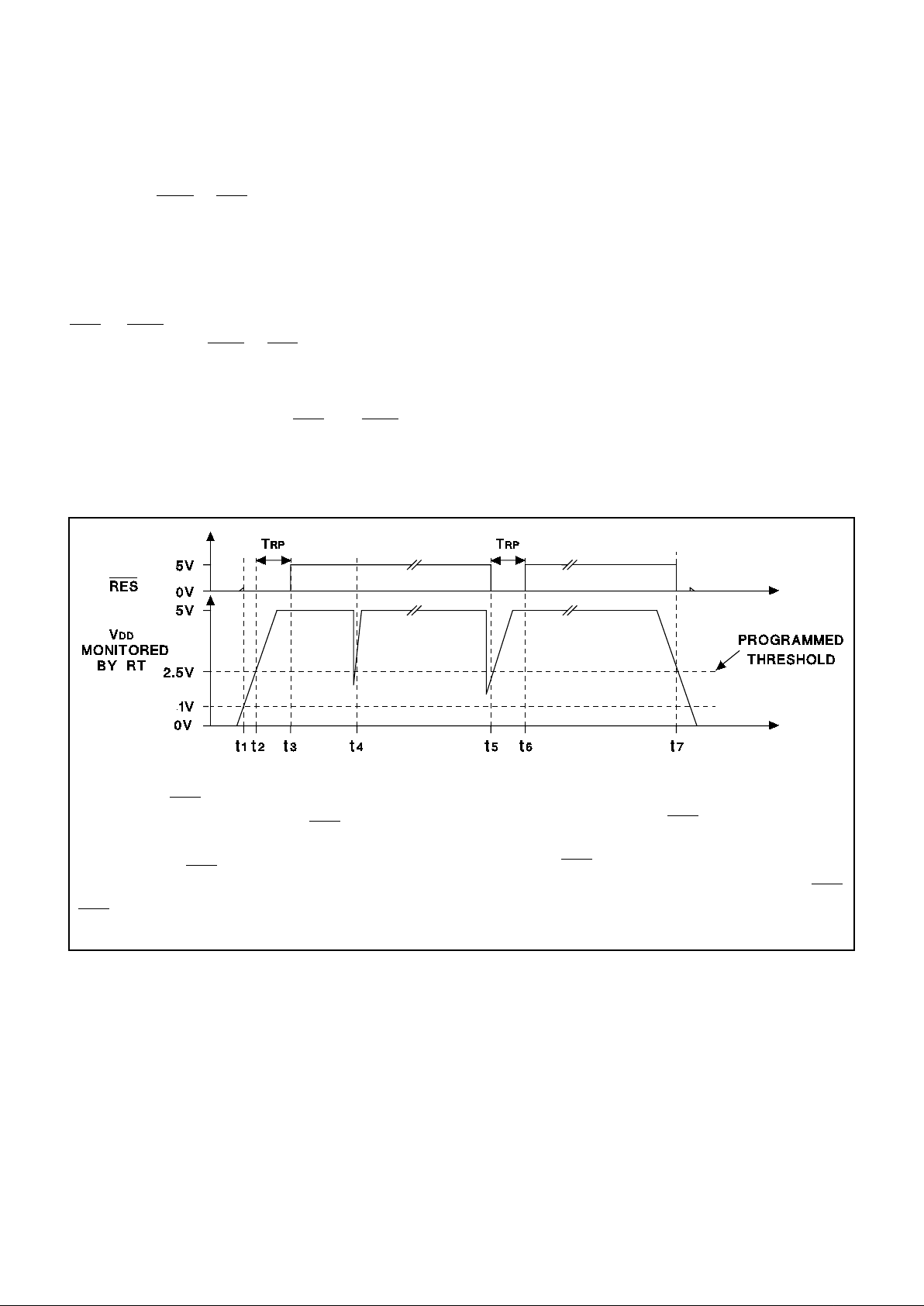
Figure 5. Reset circuit timings.
t1: VDD> 1V, RES is guaranteed low.
t2: V
DD
> programmed threshold, RES remains low for
T
RP
.
t3: T
RP
expires, RES pulls high.
t4: Voltage glitch occurs, but is filtered at the RTH pin,
RES
remains high.
t5: Voltage glitch occurs whose magnitude and duration
is greater than the RTH filter, RES
is asserted for TRP.
t6: On completion of the T
RP
pulse the RTHvoltage has
returned and RES
is pulled high.
t7: V
DD
dips below threshold (minus hysteresis), RES
is asserted.
UDG-97067
Connecting WDO to RES
In order to provide design flexibility, the reset and watch
dog circuits in the UCC3946 have separate outputs. Each
output will independently drive high or low, depending on
circuit conditions explained previously.
In some applications, it may be desirable for either the
RES
or WDO to reset the microprocessor. This can be
done by connecting WDO
to RES. If the pins try to drive
to different output levels, the low output level will domi
nate.Additional current will flow from VDD to GND during
these states. If the application cannot support additional
current (during fault conditions), RES
and WDO can be
connected to the inputs of an OR gate whose output is
connected to the microprocessor’s reset pin.
Layout Considerations
A 0.1µF capacitor connected from V
DD to GND is recom
-
mended to decouple the UCC3946 from switching tran
-
sients on the V
DD supply rail.
Since RP and WP are precision current sources, capaci
-
tors C
RP and CWP should be connected to these pins
with minimal trace length to reduce board capacitance.
Care should be taken to route any traces with high volt
age potential or high speed digital signals away from
these capacitors.
Resistors R1 and R2 generally have a high ohmic value,
traces associated with these parts should be kept short
in order to prevent any transient producing signals from
coupling into the high impedance RTH pin.
APPLICATION INFORMATION (cont.)

6
UCC1946
UCC2946
UCC3946
UNITRODE CORPORATION
7 CONTINENTAL BLVD.• MERRIMACK, NH 03054
TEL. (603) 424-2410 • FAX (603) 424-3460
0V
V
DD
t1
0V
V
DD
VDD
0V
t2 t3 t4 t5 t6 t7 t8 t9 t10 t11 t12 t13 t14
T
RP
TWP
RESET
WDI
WDO
Figure 6. Watchdog circuit timings.
APPLICATION INFORMATION (cont.)
t1: Microprocessor is reset.
t2: WDI is toggled some time after reset, but before
T
WP expires.
t3: WDI is toggled before T
WP expires.
t4: WDI is toggled before T
WP expires.
t5: WDI is not toggled before T
WP expires and WDO as-
serts low, triggering the microprocessor to enter an error recovery routine.
t6: The microprocessor’s error recovery routine is executed and WDI is toggled, reinitiating the watchdog
timer.
t7: WDI is toggled before T
WP expires.
t8: WDI is toggled before T
WP expires.
t9: RES
is momentarily triggered, RES is asserted low
for T
RP.
t10: Microprocessor is reset, RES
pulls high.
t11: WDI is toggled some time after reset, but before
T
WP expires.
t12: WDI is toggled before T
WP expires.
t13: WDI is toggled before T
WP expires.
t14: V
DD dips below the reset threshold, RES is as-
serted.
UDG-98007
 Loading...