

Page 1

Using the UCC25630-1EVM-291
User's Guide
Literature Number: SLUUBQ8B
August 2017–Revised January 2017
Page 2

Contents
1 Introduction......................................................................................................................... 5
2 Description.......................................................................................................................... 5
2.1 Typical Applications...................................................................................................... 5
2.2 Features................................................................................................................... 5
2.3 Using the EVM with UCC256302 ...................................................................................... 6
2.4 Using the EVM with UCC256303 ...................................................................................... 6
2.5 Using the EVM with UCC256304 ...................................................................................... 6
3 Performance Specifications................................................................................................... 7
4 UCC25630-1EVM-291 Schematic ............................................................................................ 8
5 Test Setup........................................................................................................................... 9
5.1 Test Equipment........................................................................................................... 9
5.2 Recommended Test Setup at No Load.............................................................................. 10
5.3 Recommended Test Setup With Load............................................................................... 11
6 List of Test Points .............................................................................................................. 11
7 List of Terminals ................................................................................................................ 12
8 Test Procedure................................................................................................................... 12
8.1 Equipment Shutdown .................................................................................................. 12
9 Performance Data and Typical Characteristic Curves ............................................................. 13
9.1 Efficiency................................................................................................................. 13
9.2 Load Regulation ........................................................................................................ 13
9.3 Output Turn On ......................................................................................................... 14
9.4 Load Transient ......................................................................................................... 15
9.5 Output Voltage Ripple.................................................................................................. 16
9.6 Burst Mode at Light Load.............................................................................................. 16
9.7 Voltage on Resonant Capacitor....................................................................................... 17
9.8 X-Cap Discharge........................................................................................................ 17
9.9 Bode Plot ................................................................................................................ 18
9.10 Switching Frequency vs. Load........................................................................................ 18
10 EVM Assembly Drawing and PCB Layout.............................................................................. 18
11 List of Materials ................................................................................................................. 21
Revision History.......................................................................................................................... 23
2
Table of Contents
Copyright © 2017, Texas Instruments Incorporated
SLUUBQ8B–August 2017–Revised January 2017
Submit Documentation Feedback
Page 3

www.ti.com
1 UCC25630-1EVM-291 Schematic......................................................................................... 8
2 UCC25630-1EVM-291 Recommended Test Setup for No Load..................................................... 10
3 UCC25630-1EVM-291 Recommended Test Setup With Load....................................................... 11
4 UCC25630-1EVM-291 Efficiency ........................................................................................ 13
5 UCC25630-1EVM-291 Load Regulation ................................................................................ 13
6 Output Turn On at 390 VDC with Full Load (10 A) .................................................................... 14
7 Output Turn On at 390 VDC with No Load ............................................................................. 14
8 No Load (0 A) to Full Load (10 A) Transient (Ch1 = I
9 Full Load (10 A) to No Load (0 A) Transient (Ch1 = I
10 Output Voltage Ripple at V
11 Burst Mode at Vin= 390-V and 100-mA Load (Ch3 = V
12 Voltage on Resonant Capacitor (Vin= 390-V and 10-A Load, Ch1 = V
13 X-Cap Discharge ........................................................................................................... 17
14 Bode Plot at V
15 Switching Frequency vs. Load (V
16 UCC25630-1EVM-291 Top Layer Assembly Drawing (Top View)................................................... 19
17 UCC25630-1EVM-291 Bottom Layer Assembly Drawing (Bottom View)........................................... 19
18 UCC25630-1EVM-291 Top Copper (Top View)........................................................................ 20
19 UCC25630-1EVM-291 Bottom Copper (Top View).................................................................... 20
List of Figures
; Ch3 = V
out
; Ch3 = V
out
= 390-V and 10-A Load ................................................................. 16
in
; Ch4 = LO).............................................. 16
out
= 390 V and 10 A Load ................................................................................ 18
in
= 390 V)............................................................................ 18
in
)................................................ 15
out
)................................................ 15
out
; Ch4 = LO)........................... 17
RES
List of Tables
1 UCC25630-1EVM-291 Specifications..................................................................................... 7
2 UCC25630-1EVM-291 Typical No Load and Standby Power ......................................................... 7
3 Test Points .................................................................................................................. 11
4 Terminals.................................................................................................................... 12
5 UCC25630-1EVM-291 List of Materials ................................................................................. 21
SLUUBQ8B–August 2017–Revised January 2017
Submit Documentation Feedback
Copyright © 2017, Texas Instruments Incorporated
List of Figures
3
Page 4

WARNING
General Texas Instruments High Voltage Evaluation (TI HV EVM) User Safety Guidelines
Always follow TI’s setup and application instructions, including use of all interface components within their
recommended electrical rated voltage and power limits. Always use electrical safety precautions to help
ensure your personal safety and those working around you. Contact TI's Product Information Center
http://support/ti./com for further information.
Save all warnings and instructions for future reference.
Failure to follow warnings and instructions may result in personal injury, property damage, or
death due to electrical shock and burn hazards.
The term TI HV EVM refers to an electronic device typically provided as an open framed, unenclosed
printed circuit board assembly. It is intended strictly for use in development laboratory environments,
solely for qualified professional users having training, expertise and knowledge of electrical safety
risks in development and application of high voltage electrical circuits. Any other use and/or
application are strictly prohibited by Texas Instruments. If you are not suitable qualified, you should
immediately stop from further use of the HV EVM.
1. Work Area Safety
1. Keep work area clean and orderly.
2. Qualified observer(s) must be present anytime circuits are energized.
3. Effective barriers and signage must be present in the area where the TI HV EVM and its interface
electronics are energized, indicating operation of accessible high voltages may be present, for the
purpose of protecting inadvertent access.
4. All interface circuits, power supplies, evaluation modules, instruments, meters, scopes and other
related apparatus used in a development environment exceeding 50Vrms/75VDC must be
electrically located within a protected Emergency Power Off EPO protected power strip.
5. Use stable and nonconductive work surface.
6. Use adequately insulated clamps and wires to attach measurement probes and instruments. No
freehand testing whenever possible.
2. Electrical Safety
As a precautionary measure, it is always a good engineering practice to assume that the entire EVM
may have fully accessible and active high voltages.
1. De-energize the TI HV EVM and all its inputs, outputs and electrical loads before performing any
electrical or other diagnostic measurements. Revalidate that TI HV EVM power has been safely
de-energized.
2. With the EVM confirmed de-energized, proceed with required electrical circuit configurations,
wiring, measurement equipment connection, and other application needs, while still assuming the
EVM circuit and measuring instruments are electrically live.
3. After EVM readiness is complete, energize the EVM as intended.
WARNING: WHILE THE EVM IS ENERGIZED, NEVER TOUCH THE EVM OR ITS ELECTRICAL
CIRCUITS AS THEY COULD BE AT HIGH VOLTAGES CAPABLE OF CAUSING ELECTRICAL
SHOCK HAZARD.
3. Personal Safety
1. Wear personal protective equipment (for example, latex gloves or safety glasses with side shields)
or protect EVM in an adequate lucent plastic box with interlocks to protect from accidental touch.
Limitation for safe use:
EVMs are not to be used as all or part of a production unit.
www.ti.com
4
List of Tables
Copyright © 2017, Texas Instruments Incorporated
SLUUBQ8B–August 2017–Revised January 2017
Submit Documentation Feedback
Page 5

1 Introduction
This EVM, UCC25630-1EVM-291, is used to help evaluate the UCC256301 LLC control device in digital
TV SMPS, AC-DC power adapter, LED lighting, etc. applications and then to aid their design. The EVM is
a standalone LLC resonant half-bridge DC-DC power converter. The EVM, UCC25630-1EVM-291, can be
used as it is delivered without additional work to evaluate an LLC resonant half-bridge DC-DC converter.
This user’s guide provides basic evaluation instruction from a viewpoint of system operation in standalone
LLC resonant half-bridge DC-DC power converter.
2 Description
UCC25630-1EVM-291 is an EVM for an LLC resonant half-bridge DC-DC power converter with LLC
controller UCC256301. UCC25630-1EVM-291 accepts DC line input from 340 VDC to 410 VDC, AC input
voltage from 85 VAC to 264 VAC, and a nominal output of 12 VDC with a full-load output power of 120 W,
or a full output current of 10 A.
NOTE: This EVM does not have an input fuse, and relies on an input current limit from its input
voltage source.
User's Guide
SLUUBQ8B–August 2017–Revised January 2017
Using the UCC25630-1EVM-291
2.1 Typical Applications
• Digital TV SMPS
• AC-DC Power Adapters
• Enterprise Server Applications
• LED Lighting Applications
2.2 Features
• Hybrid Hysteretic Controlled LLC Resonant Half-Bridge DC-DC Power Conversion
• DC Line Input from 340 VDC to 410 VDC
• AC Input Voltage from 85 VDC to 264 VAC
• Regulated 12-VDC Output, from No-Load to Full-Load
• Full-Load Power of 120 W, or Full-Load Current of 10 A
• High Efficiency
• Optimized Low Power Features Enable Extremely Low Standby Power
• Advanced Burst Mode with Adaptive Threshold
• Improved Capacitive Region Avoidance Scheme
• Adaptive Dead-Time
• X-Capacitor Discharge
• Over Temperature, Output Over Voltage, and Three Level Over Current Protections
• Test Points to Facilitate Device and Topology Evaluation
SLUUBQ8B–August 2017–Revised January 2017
Submit Documentation Feedback
Copyright © 2017, Texas Instruments Incorporated
Using the UCC25630-1EVM-291
5
Page 6

Description
2.3 Using the EVM with UCC256302
To use this EVM with UCC256302:
• Replace U1 with UCC256302
• Remove D1, D2
• Connect TP10 to TP5
2.4 Using the EVM with UCC256303
UCC25630-1EVM-291 is designed for UCC256301. With a slightly modification, this EVM can be used for
UCC256303. To use this EVM with UCC256303:
• Replace U1 with UCC256303
• Remove R11, D4
• Connect pin1 (HV) of U1 to PGND
• Connect external bias (11.25V - 26V) to TP21
2.5 Using the EVM with UCC256304
To use this EVM with UCC256304:
• Replace U1 with UCC256304
• Change R4 to 44.2 kΩ
www.ti.com
6
Using the UCC25630-1EVM-291
Copyright © 2017, Texas Instruments Incorporated
SLUUBQ8B–August 2017–Revised January 2017
Submit Documentation Feedback
Page 7
www.ti.com
3 Performance Specifications
Table 1. UCC25630-1EVM-291 Specifications
PARAMETER TEST CONDITIONS MIN TYP MAX UNITS
INPUT CHARACTERISTICS
DC voltage range 340 390 410 VDC
AC voltage range 85 264 VAC
AC voltage frequency 47 63 Hz
Input DC UVLO On 320 VDC
Input DC UVLO Off 140 VDC
Input DC current Input = 340 VDC, full load = 10 A 0.383 A
Input DC current Input = 390 VDC, full load = 10 A 0.331 A
Input DC current Input = 410 VDC, full load = 10 A 0.315 A
OUTPUT CHARACTERISTICS
V
I
OUT
OUT
Output voltage No load to full load = 10 A 12 VDC
Output load current 340 to 410 VDC 10 A
Output voltage ripple 390 VDC and full load = 10 A 130 mVpp
SYSTEM CHARACTERISTICS
Switching frequency 53 160 kHz
Peak efficiency 390 VDC, load = 8 A 92.9%
Operating temperature Natural convection 25 ºC
Performance Specifications
Table 2. UCC25630-1EVM-291 Typical No Load and Standby Power
VIN= 390 V
INPUT POWER (mW) OUTPUT POWER (mW) POWER LOSS (mW)
39.7 0 39.7
163.7 103.0 60.6
295.0 201.2 93.8
421.7 299.0 122.7
548.0 401.6 146.4
674.0 498.6 175.4
SLUUBQ8B–August 2017–Revised January 2017
Submit Documentation Feedback
Copyright © 2017, Texas Instruments Incorporated
Using the UCC25630-1EVM-291
7
Page 8
~
3
+
1
~
2
4
D3
GBU8J-BP
1uF
C3
1uF
C4
MURA160T3G
D1
MURA160T3G
D2
0.47µF
C6
HV1VCC
3
BLK
4
FB
5
ISNS6VCR7BW8LL/SS
9
LO
10
GND
11
RVCC
12
HB
14
HO
15
HS
16
U1
UCC25630-1DDB
470µF
C20
470µF
C21
470µF
C22
470µF
C23
TP4
TP1
TP3
TP5
TP2
TP10
TP7
TP12
TP11
TP23
HS2
HS1
PGND
SGND
PGND
PGND
EARTH
PGND
HS3
HS4
SGND
SGND
Q1
SPW20N60CFD
Q2
SPW20N60CFD
10pF
C29
DNP
0.047µF
C28
10.0k
R22
SGND
PGND
147k
R25
16.9k
R26
SGND
1
2 3
U4
TLVH431AQPK
6.04k
R20
2.2
R16
2.2µF
C18
LO
HO
HO
LO
HS
HS
1
2
4
3
U2
VO618A-3
42.2k
R17
10.0k
R18
PGND
3.9pF
C13
2.2µF
C12
4.7µF
C15
4.99M
R1
4.99MR24.99M
R3
140k
R4
PGND
BLK
BLK
PGND
0.022µF
C7
PGND
TP19
120µF
C16
0.15µF
C17
220pF
C5
TP6
RV1
MOV-14D621K
12V Vout
85V - 264V AC Input
TP8
TP9
22µF
C24
0.022µF
C8
1.5 µF
C2
402k
R15
732k
R14
357
R13
PGND
PGND
1.65k
R10
1.65k
R9
0
R24
TP17
TP18
10.0
R5
10.0
R6
5.11k
R7
5.11k
R8
10.0M
R28
TP13
60V
D4
6.04k
R23
NC8NC
11
5
1103
1279
6
NC2NC
4
T1
J2
J3
+
-
+
-
150pF
C11
TP20
TP16
TP15
1
2
4
3
U3
VO618A-3
PGND
2.00k
R19
SGND
J4
External disable
22µF
C25
22µF
C26
22µF
C27
123
D6
STPS41H100CTY
123
D7
STPS41H100CTY
D5
ES1JAF
47µF
C1
J1
10.0M
R27
10.0M
R12
10.0M
R29
TP22
1.65k
R11
J5
3300pF
C30
DNP
1.00
R30
D8
1N4148W-7-F
D9
1N4148W-7-F
TP14
TP21
4.7µF
C14
0
R32
10pF
C19
DNP
10.0k
R21
D10
MMSZ5234B-7-F
0.015µF
C10
150pF
C9
1.00
R31
3
4
NC1NC
2
NC5NC
6
50µHL1
Copyright © 2017, Texas Instruments Incorporated
UCC25630-1EVM-291 Schematic
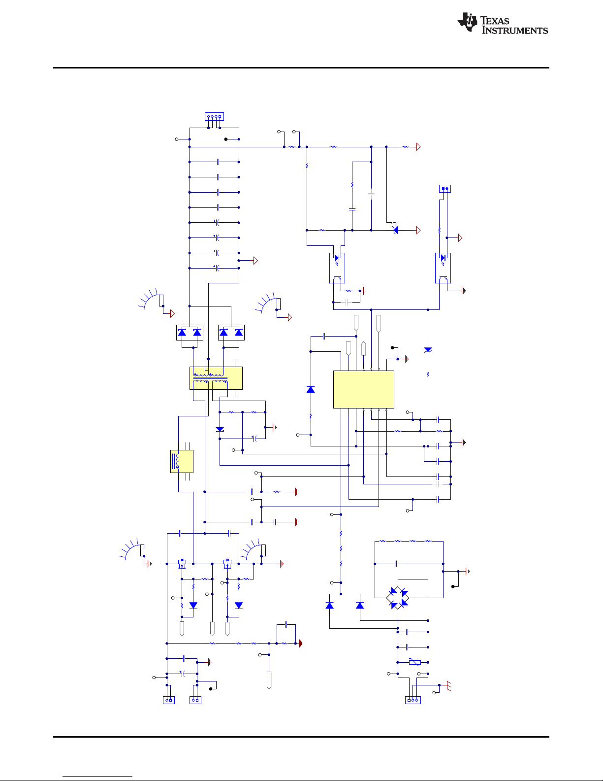
4 UCC25630-1EVM-291 Schematic
www.ti.com
8
Using the UCC25630-1EVM-291
Figure 1. UCC25630-1EVM-291 Schematic
Copyright © 2017, Texas Instruments Incorporated
SLUUBQ8B–August 2017–Revised January 2017
Submit Documentation Feedback
Page 9

www.ti.com
5 Test Setup
5.1 Test Equipment
DC Voltage Source: capable of 340 VDC to 410 VDC, adjustable, with minimum power rating 200 W, or
current rating not less than 1 A, with current limit function. The DC voltage source to be used should meet
IEC60950 reinforced insulation requirement.
AC Voltage Source: capable of single-phase output AC voltage 85 VAC to 264 VAC, 47 Hz to 63 Hz,
adjustable with minimum power rating 100 W. The AC voltage source to be used should meet IEC60950
reinforced insulation requirement.
DC Digital Multimeter: One unit capable of 0-VDC to 450-VDC input range, four digit display preferred;
and one unit capable of 0-VDC to 20-VDC input range, four digit display preferred.
Output Load: DC load capable of receiving 0 VDC to 20 VDC, 0 A to 15 A, and 0 W to 200 W or greater,
with the capability to display things such as load current and load power.
Current Meter: DC, optional in case the load has no display, one unit, capable of 0 A to 15 A. If you want
to measure standby power, the current meter needs to have a time averaging function.
Oscilloscope: capable of 500-MHz full bandwidth, digital or analog, if digital, 5 Gs/s or better.
Fan: 200-LFM to 400-LFM forced air cooling is recommended, but not required.
Recommended Wire Gauge: capable of 15 A, or better than #14 AWG, with the total length of wire less
than 8 feet (4 feet input and 4 feet return).
Test Setup
SLUUBQ8B–August 2017–Revised January 2017
Submit Documentation Feedback
Copyright © 2017, Texas Instruments Incorporated
Using the UCC25630-1EVM-291
9
Page 10

Test Setup
5.2 Recommended Test Setup at No Load
Figure 2 shows the equipment setup for testing at no load. It is important to note that in this setup, current
drawn by the voltage meter does not flow through the current meter.
Also, do not connect oscilloscope probes or any other sensing devices to the unit while measuring no-load
power, as these can provide a path for common mode current to flow. This causes an error in the
measurements.
During the no-load test, the current meter should be set to long-averaging mode and a few minutes should
be allowed for the reading to be accurate. Additionally, an appropriate current scale factor should be used.
www.ti.com
Figure 2. UCC25630-1EVM-291 Recommended Test Setup for No Load
10
Using the UCC25630-1EVM-291
Copyright © 2017, Texas Instruments Incorporated
SLUUBQ8B–August 2017–Revised January 2017
Submit Documentation Feedback
Page 11
www.ti.com
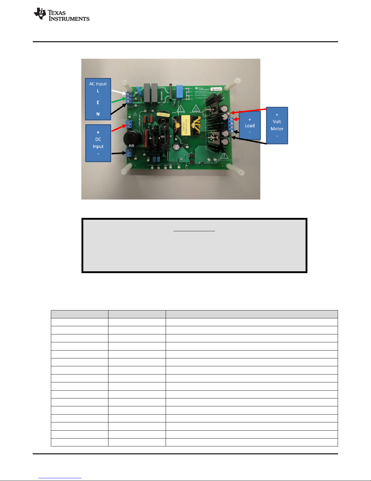
5.3 Recommended Test Setup With Load
Figure 3. UCC25630-1EVM-291 Recommended Test Setup With Load
Test Setup
High voltages that may cause injury exist on this evaluation
module (EVM). Please ensure all safety procedures are followed
when working on this EVM. Never leave a powered EVM
unattended.
6 List of Test Points
TEST POINTS NAME DESCRIPTION
TP1 EARTH AC earth
TP2 VIN_N Input voltage return terminal
TP3 AC_N AC neutral
TP4 AC_L AC line
TP5 VIN_P Input voltage positive terminal
TP6 BLK Input voltage sensing
TP7 HS Primary-side switch node, or the intersection of Q1 and Q2
TP8 HO Primary-side high side MOSFET gate, Q1
TP9 LO Primary-side low side MOSFET gate, Q2
TP10 AC_R AC rectifier output
TP11 VOUT_P Output voltage positive terminal
TP12 HV High-voltage start pin
TP13 PGND Primary-side ground
TP14 PGND Primary-side ground
TP15 VCR Resonant capacitor voltage sense
TP16 ISNS Resonant current sense
WARNING
Table 3. Test Points
SLUUBQ8B–August 2017–Revised January 2017
Submit Documentation Feedback
Copyright © 2017, Texas Instruments Incorporated
Using the UCC25630-1EVM-291
11
Page 12

List of Terminals
TEST POINTS NAME DESCRIPTION
TP17 INJECT1 Small signal injection terminal
TP18 INJECT2 Small signal injection terminal
TP19 BW Bias winding voltage sense
TP20 RVCC Regulated 12-V supply
TP21 VCC Supply input
TP22 LL/SS Soft-start and light-load burst mode threshold
TP23 VOUT_N Output voltage return terminal
7 List of Terminals
TERMINAL NAME DESCRIPTION
J1 AC Input 3-pin, AC power input, 85 V to 265 V
J2 VIN_P Input voltage positive terminal
J3 VIN_N Input voltage return terminal
J4 DISABLE External disable terminal
J5 VOUT Output voltage terminal, 4-pin
www.ti.com
Table 3. Test Points (continued)
Table 4. Terminals
8 Test Procedure
1. Refer to Figure 3 for basic setup. The required equipment for this measurement is listed in Section 5.1.
2. Before making electrical connections, visually check the board to make sure there are no suspected
spots of damage.
3. Keep the DC voltage source output off, connect it to J2 (+) and J3 (-). The DC voltage source should
be isolated and meet the IEC60950 requirement. Set the DC output voltage within the range specified
in Table 1, between 340 VDC and 410 VDC; set the DC source current limit to 1 A.
NOTE: The board has no fuse installed and relies on the external voltage source current limit to
ensure circuit protection.
4. Connect an electronic load set to either constant current mode or constant resistance mode. The load
current range is from 0 A to 10 A.
5. Keep the AC voltage source output off, connect it to J1 with AC_line to J1-1, AC_earth to J1-2,
AC_neutral to J1-3. The AC voltage source should be isolated and meet the IEC60950 requirement.
Set the AC output voltage in the range specified in Table 1, between 85 VAC and 264 VAC; set the AC
source current limit to 200 mA.
6. If the load does not have a current or a power display, a current meter needs to be inserted between
the load and the board.
7. Connect a voltage meter across the load and set the meter’s scale to 20 VDC.
8. Turn on the AC voltage source output.
9. Turn on the DC voltage source output. Then the measurements can be made.
8.1 Equipment Shutdown
1. Shut down AC voltage source.
2. Shut down DC voltage source.
3. Shut down electronic load.
12
Using the UCC25630-1EVM-291
Copyright © 2017, Texas Instruments Incorporated
SLUUBQ8B–August 2017–Revised January 2017
Submit Documentation Feedback
Page 13

I
out
(A)
V
out
(V)
0 1 2 3 4 5 6 7 8 9 10
12.012
12.014
12.016
12.018
12.02
12.022
12.024
D002
I
out
(A)
Efficiency (%)
0 1 2 3 4 5 6 7 8 9 10
77
79
81
83
85
87
89
91
93
95
D001
www.ti.com
Performance Data and Typical Characteristic Curves
9 Performance Data and Typical Characteristic Curves
Figure 4 through Figure 15 present typical performance curves for UCC25630-1EVM-291.
9.1 Efficiency
Figure 4. UCC25630-1EVM-291 Efficiency
9.2 Load Regulation
Figure 5. UCC25630-1EVM-291 Load Regulation
SLUUBQ8B–August 2017–Revised January 2017
Submit Documentation Feedback
Copyright © 2017, Texas Instruments Incorporated
Using the UCC25630-1EVM-291
13
Page 14

Performance Data and Typical Characteristic Curves
9.3 Output Turn On
www.ti.com
Figure 6. Output Turn On at 390 VDC with Full Load (10 A)
Figure 7. Output Turn On at 390 VDC with No Load
14
Using the UCC25630-1EVM-291
Copyright © 2017, Texas Instruments Incorporated
SLUUBQ8B–August 2017–Revised January 2017
Submit Documentation Feedback
Page 15

www.ti.com
9.4 Load Transient
Performance Data and Typical Characteristic Curves
Figure 8. No Load (0 A) to Full Load (10 A) Transient (Ch1 = I
; Ch3 = V
out
out
)
Figure 9. Full Load (10 A) to No Load (0 A) Transient (Ch1 = I
SLUUBQ8B–August 2017–Revised January 2017
Submit Documentation Feedback
Copyright © 2017, Texas Instruments Incorporated
; Ch3 = V
out
Using the UCC25630-1EVM-291
out
)
15
Page 16

Performance Data and Typical Characteristic Curves
9.5 Output Voltage Ripple
www.ti.com
Figure 10. Output Voltage Ripple at Vin= 390-V and 10-A Load
9.6 Burst Mode at Light Load
Figure 11. Burst Mode at Vin= 390-V and 100-mA Load (Ch3 = V
16
Using the UCC25630-1EVM-291
Copyright © 2017, Texas Instruments Incorporated
; Ch4 = LO)
out
SLUUBQ8B–August 2017–Revised January 2017
Submit Documentation Feedback
Page 17

www.ti.com
9.7 Voltage on Resonant Capacitor
Performance Data and Typical Characteristic Curves
Figure 12. Voltage on Resonant Capacitor (Vin= 390-V and 10-A Load, Ch1 = V
9.8 X-Cap Discharge
; Ch4 = LO)
RES
SLUUBQ8B–August 2017–Revised January 2017
Submit Documentation Feedback
Figure 13. X-Cap Discharge
Copyright © 2017, Texas Instruments Incorporated
Using the UCC25630-1EVM-291
17
Page 18

Load Current (A)
Frequency (kHz)
1 2 3 4 5 6 7 8 9 10
82.5
85
87.5
90
92.5
95
97.5
D003
Performance Data and Typical Characteristic Curves
www.ti.com
(Test condition: VAC= 264 V
, disconnected AC randomly, discharge time from 373 VAC to below 30 V:
RMS
700 ms)
9.9 Bode Plot
Figure 14. Bode Plot at Vin= 390 V and 10 A Load
9.10 Switching Frequency vs. Load
Figure 15. Switching Frequency vs. Load (Vin= 390 V)
10 EVM Assembly Drawing and PCB Layout
Figure 16 through Figure 19 show the design of the UCC25630-1EVM-291 printed circuit board. PCB
dimensions: L x W = 5.9 x 4.8 in, PCB material: FR4 or compatible, two layers and 2 oz copper on each
layer.
18
Using the UCC25630-1EVM-291
Copyright © 2017, Texas Instruments Incorporated
SLUUBQ8B–August 2017–Revised January 2017
Submit Documentation Feedback
Page 19

www.ti.com
EVM Assembly Drawing and PCB Layout
Figure 16. UCC25630-1EVM-291 Top Layer Assembly Drawing (Top View)
Figure 17. UCC25630-1EVM-291 Bottom Layer Assembly Drawing (Bottom View)
SLUUBQ8B–August 2017–Revised January 2017
Submit Documentation Feedback
Copyright © 2017, Texas Instruments Incorporated
Using the UCC25630-1EVM-291
19
Page 20

EVM Assembly Drawing and PCB Layout
www.ti.com
Figure 18. UCC25630-1EVM-291 Top Copper (Top View)
Figure 19. UCC25630-1EVM-291 Bottom Copper (Top View)
20
Using the UCC25630-1EVM-291
Copyright © 2017, Texas Instruments Incorporated
SLUUBQ8B–August 2017–Revised January 2017
Submit Documentation Feedback
Page 21

www.ti.com
11 List of Materials
DES QTY DESCRIPTION PART NUMBER MANUFACTURER
PCB1 1 Printed Circuit Board SV601291 Any
C1 1 Capacitor, aluminum, 47 µF, 450 V, ±20%, 2.82 ohm, TH B43501A5476M000 TDK
C2 1 Capacitor, film, 1.5uF, 450V, ±10%, TH ECQ-E2W155KH Panasonic
C3, C4 2 Capacitor, film, 1uF, 275V, ±20%, TH R46KN410000P0M Kemet
C5 1 Capacitor, ceramic, 220 pF, 50 V, ±10%, X7R, 0603 GRM188R71H221KA
C6 1 Capacitor, film, 0.47 µF, 630 V, ±10%, TH B32922C3474K TDK
C7, C8 2 Capacitor, film, 0.022 µF, 630 V, ±5%, TH ECWF6223JL Panasonic
C9, C11 2 Capacitor, film, 150 pF, 630 V, ±5%, TH PFR5151J630J11L4B
C10 1 Capacitor, ceramic, 0.015 µF, 25 V, ±5%, C0G/NP0, 0603 C0603C153J3GACTU Kemet
C12 1 Capacitor, ceramic, 2.2 µF, 35 V, ±10%, X5R, 0603 GRM188R6YA225KA
C13 1 Capacitor, ceramic, 3.9 pF, 50 V, ±6%, C0G/NP0, 0603 06035A3R9CAT2A AVX
C14, C15 2 Capacitor, ceramic, 4.7 µF, 16 V, ±10%, X5R, 0603 GRM188R61C475KAAJMuRata
List of Materials
Table 5. UCC25630-1EVM-291 List of Materials
MuRata
01D
Kemet
ULK
MuRata
12D
C16 1 Capacitor, aluminum, 120 µF, 63 V, ± 20%, 0.194 ohm,
C17 1 Capacitor, ceramic, 0.15 µF, 16 V, ±20%, Y5V, 0603 C0603C154Z4VACTU Kemet
C18 1 Capacitor, ceramic, 2.2 µF, 16 V, ±10%, X7R, 1206 C1206C225K4RACTU Kemet
C19 0 Capacitor, ceramic, 10 pF, 50 V, ±5%, C0G/NP0, 0603 06035A100JAT2A AVX
C20, C21,
C22, C23
C24, C25,
C26, C27
C28 1 Capacitor, ceramic, 0.047 µF, 16 V, ±10%, X7R, 0603 GRM188R71C473KA
C29 0 Capacitor, ceramic, 10 pF, 50 V, ±5%, C0G/NP0, 0603 06035A100JAT2A AVX
C30 0 Capacitor, ceramic, 3300 pF, 50 V, ±5%, C0G/NP0, 0603 GRM1885C1H332JA01DMuRata
D1, D2 2 Diode, Ultrafast, 600 V, 1 A, SMA MURA160T3G ON Semiconductor
D3 1 Diode, Switching-Bridge, 420 V, 8 A, TH GBU8J-BP Micro Commercial
D4 1 Diode, Schottky, 60 V, 1 A, AEC-Q101, SMB STPS160UY STMicroelectronics
D5 1 Diode, Ultrafast, 600 V, 1 A, AEC-Q101, SMAF ES1JAF Fairchild
D6, D7 2 Diode, Schottky, 100 V, 20 A, AEC-Q101, TH STPS41H100CTY STMicroelectronics
D8, D9 2 Diode, Ultrafast, 100 V, 0.15 A, SOD-123 1N4148W-7-F Diodes Inc.
D10 1 Diode, Zener, 6.2 V, 500 mW, SOD-123 MMSZ5234B-7-F Diodes Inc.
H1, H3,
H5, H7
H2, H4,
H6, H8
H9, H11 2 TO-220 mounting kit 4880SG Aavid Thermalloy
H10, H12 2 TO-247 mounting kit 4880SG Aavid Thermalloy
H13, H14 2 Large thermal pad to substitute for the smaller one in the
HS1,
HS2,
HS3, HS4
J1 1 Terminal block, 5.08 mm, 3x1, brass, TH ED120/3DS On-Shore Technology
AEC-Q200 Grade 2, TH
4 Capacitor, aluminum, 470 µF, 35 V, ±20%, TH 35ZL470MEFC10X20 Rubycon
4 Capacitor, ceramic, 22 µF, 35 V, ± 20%, X5R, 0805 C2012X5R1V226M12
4 Hex standoff 1-1/2" L #6-32 nylon 4824 Keystone
4 Hex standoff 0.5"L #6-32 nylon 1903C Keystone
TO-247 Mounting Kit
4 Heatsink TO-220 w/pins 1.5" tall 531102B02500G Aavid
EEU-FC1J121 Panasonic
TDK
5AC
MuRata
01D
Components
Semiconductor
SP900S-0.009-00-104 Bergquist
SLUUBQ8B–August 2017–Revised January 2017
Submit Documentation Feedback
Copyright © 2017, Texas Instruments Incorporated
Using the UCC25630-1EVM-291
21
Page 22

List of Materials
DES QTY DESCRIPTION PART NUMBER MANUFACTURER
J2, J3 2 Terminal block, 5.08 mm, 2x1, brass, TH ED120/2DS On-Shore Technology
J4 1 Header, 100 mil, 2 x 1, tin, TH PEC02SAAN Sullins Connector
J5 1 Terminal block, 5.08 mm, 4x1, brass, TH ED120/4DS On-Shore Technology
L1 1 Inductor, 50 µH, 0.023 Ω, TH RLTI-1234 Renco Electronics
Q1, Q2 2 MOSFET, N-channel, 650 V, 20.7 A, TO-247 SPW20N60CFD Infineon Technologies
R1, R2,
R3
R4 1 Resistor, 140 kΩ, 1%, 0.1 W, 0603 CRCW0603140KFKEAVishay-Dale
R5, R6 2 Resistor, 10.0 Ω, 1%, 0.125 W, 0805 CRCW080510R0FKEAVishay-Dale
R7, R8 2 Resistor, 5.11 kΩ, 1%, 0.1W, 0603 CRCW06035K11FKEAVishay-Dale
www.ti.com
Table 5. UCC25630-1EVM-291 List of Materials (continued)
Solutions
3 Resistor, 4.99 MΩ, 1%, 0.25 W, 1206 CRCW12064M99FKEAVishay-Dale
R9, R10,
R11
R12, R27,
R28, R29
R13 1 Resistor, 357 Ω, 1%, 0.25 W, 1206 CRCW1206357RFKEAVishay-Dale
R14 1 Resistor, 732 kΩ, 1%, 0.1 W, 0603 CRCW0603732KFKEAVishay-Dale
R15 1 Resistor, 402 kΩ, 1%, 0.1 W, 0603 CRCW0603402KFKEAVishay-Dale
R16 1 Resistor, 2.2 Ω, 5%, 0.1 W, 0603 CRCW06032R20JNEAVishay-Dale
R17 1 Resistor, 42.2 kΩ, 1%, 0.1 W, 0603 CRCW060342K2FKEAVishay-Dale
R18, R21,
R22
R19 1 Resistor, 2.00 kΩ, 1%, 0.1 W, 0603 CRCW06032K00FKEAVishay-Dale
R20, R23 2 Resistor, 6.04 kΩ, 1%, 0.1 W, 0603 CRCW06036K04FKEAVishay-Dale
R24, R32 2 Resistor, 0 Ω, 5%, 0.1 W, 0603 CRCW06030000Z0EAVishay-Dale
R25 1 Resistor, 147 kΩ, 1%, 0.1 W, 0603 CRCW0603147KFKEAVishay-Dale
R26 1 Resistor, 16.9 kΩ, 1%, 0.1 W, 0603 CRCW060316K9FKEAVishay-Dale
R30, R31 2 Resistor, 1.00 Ω, 1%, 0.125 W, 0805 CRCW08051R00FKEAVishay-Dale
3 Resistor, 1.65 kΩ, 1%, 0.25 W, 1206 CRCW12061K65FKEAVishay-Dale
4 Resistor, 10.0 MΩ, 1%, 0.25 W, 1206 CRCW120610M0FKEAVishay-Dale
3 Resistor, 10.0 kΩ, 1%, 0.1 W, 0603 CRCW060310K0FKEAVishay-Dale
RV1 1 Varistor 558 V 4.5KA, TH MOV-14D621K Bourns
T1 1 Transformer, 840 µH, TH RLTI-1233 Renco Electronics
22
Using the UCC25630-1EVM-291
SLUUBQ8B–August 2017–Revised January 2017
Submit Documentation Feedback
Copyright © 2017, Texas Instruments Incorporated
Page 23

www.ti.com
Revision History
Table 5. UCC25630-1EVM-291 List of Materials (continued)
DES QTY DESCRIPTION PART NUMBER MANUFACTURER
TP1, TP3,
TP4, TP5,
TP6, TP7,
TP8, TP9,
TP10,
TP11,
TP12,
TP15,
TP16,
TP17,
TP18,
TP19,
TP20,
TP21,
TP22
TP2,
TP13,
TP14,
TP23
U1 1 Enhanced LLC Resonant Controller with Driver,
U2, U3 2 Optocoupler, 5.3 kV, 50-600% CTR, TH VO618A-3 Vishay-Semiconductor
U4 1 Low-Voltage Adjustable Precision Shunt Regulator, 80
FID1,
FID2,
FID3,
FID4,
FID5,
FID6
19 Test point, multipurpose, white, TH 5012 Keystone
4 Test point, multipurpose, black, TH 5011 Keystone
UCC256301DDB Texas Instruments
DDB0014A
TLVH431AQPK Texas Instruments
mA, -40 to 125 degC, 3-pin SOT-89 (PK), Green (RoHS &
no Sb/Br)
0 Fiducial mark. There is nothing to buy or mount. N/A N/A
Revision History
NOTE: Page numbers for previous revisions may differ from page numbers in the current version.
Changes from A Revision (September 2017) to B Revision .......................................................................................... Page
• Added Using the EVM with UCC256302 section 2.3................................................................................. 6
Changes from Original (August 2017) to A Revision ..................................................................................................... Page
• Added Using the EVM with UCC256303 section 2.4................................................................................. 6
• Added Using the EVM with UCC256304 section 2.5................................................................................. 6
SLUUBQ8B–August 2017–Revised January 2017
Submit Documentation Feedback
Copyright © 2017, Texas Instruments Incorporated
Revision History
23
Page 24

IMPORTANT NOTICE FOR TI DESIGN INFORMATION AND RESOURCES
Texas Instruments Incorporated (‘TI”) technical, application or other design advice, services or information, including, but not limited to,
reference designs and materials relating to evaluation modules, (collectively, “TI Resources”) are intended to assist designers who are
developing applications that incorporate TI products; by downloading, accessing or using any particular TI Resource in any way, you
(individually or, if you are acting on behalf of a company, your company) agree to use it solely for this purpose and subject to the terms of
this Notice.
TI’s provision of TI Resources does not expand or otherwise alter TI’s applicable published warranties or warranty disclaimers for TI
products, and no additional obligations or liabilities arise from TI providing such TI Resources. TI reserves the right to make corrections,
enhancements, improvements and other changes to its TI Resources.
You understand and agree that you remain responsible for using your independent analysis, evaluation and judgment in designing your
applications and that you have full and exclusive responsibility to assure the safety of your applications and compliance of your applications
(and of all TI products used in or for your applications) with all applicable regulations, laws and other applicable requirements. You
represent that, with respect to your applications, you have all the necessary expertise to create and implement safeguards that (1)
anticipate dangerous consequences of failures, (2) monitor failures and their consequences, and (3) lessen the likelihood of failures that
might cause harm and take appropriate actions. You agree that prior to using or distributing any applications that include TI products, you
will thoroughly test such applications and the functionality of such TI products as used in such applications. TI has not conducted any
testing other than that specifically described in the published documentation for a particular TI Resource.
You are authorized to use, copy and modify any individual TI Resource only in connection with the development of applications that include
the TI product(s) identified in such TI Resource. NO OTHER LICENSE, EXPRESS OR IMPLIED, BY ESTOPPEL OR OTHERWISE TO
ANY OTHER TI INTELLECTUAL PROPERTY RIGHT, AND NO LICENSE TO ANY TECHNOLOGY OR INTELLECTUAL PROPERTY
RIGHT OF TI OR ANY THIRD PARTY IS GRANTED HEREIN, including but not limited to any patent right, copyright, mask work right, or
other intellectual property right relating to any combination, machine, or process in which TI products or services are used. Information
regarding or referencing third-party products or services does not constitute a license to use such products or services, or a warranty or
endorsement thereof. Use of TI Resources may require a license from a third party under the patents or other intellectual property of the
third party, or a license from TI under the patents or other intellectual property of TI.
TI RESOURCES ARE PROVIDED “AS IS” AND WITH ALL FAULTS. TI DISCLAIMS ALL OTHER WARRANTIES OR
REPRESENTATIONS, EXPRESS OR IMPLIED, REGARDING TI RESOURCES OR USE THEREOF, INCLUDING BUT NOT LIMITED TO
ACCURACY OR COMPLETENESS, TITLE, ANY EPIDEMIC FAILURE WARRANTY AND ANY IMPLIED WARRANTIES OF
MERCHANTABILITY, FITNESS FOR A PARTICULAR PURPOSE, AND NON-INFRINGEMENT OF ANY THIRD PARTY INTELLECTUAL
PROPERTY RIGHTS.
TI SHALL NOT BE LIABLE FOR AND SHALL NOT DEFEND OR INDEMNIFY YOU AGAINST ANY CLAIM, INCLUDING BUT NOT
LIMITED TO ANY INFRINGEMENT CLAIM THAT RELATES TO OR IS BASED ON ANY COMBINATION OF PRODUCTS EVEN IF
DESCRIBED IN TI RESOURCES OR OTHERWISE. IN NO EVENT SHALL TI BE LIABLE FOR ANY ACTUAL, DIRECT, SPECIAL,
COLLATERAL, INDIRECT, PUNITIVE, INCIDENTAL, CONSEQUENTIAL OR EXEMPLARY DAMAGES IN CONNECTION WITH OR
ARISING OUT OF TI RESOURCES OR USE THEREOF, AND REGARDLESS OF WHETHER TI HAS BEEN ADVISED OF THE
POSSIBILITY OF SUCH DAMAGES.
You agree to fully indemnify TI and its representatives against any damages, costs, losses, and/or liabilities arising out of your noncompliance with the terms and provisions of this Notice.
This Notice applies to TI Resources. Additional terms apply to the use and purchase of certain types of materials, TI products and services.
These include; without limitation, TI’s standard terms for semiconductor products http://www.ti.com/sc/docs/stdterms.htm), evaluation
modules, and samples (http://www.ti.com/sc/docs/sampterms.htm).
Mailing Address: Texas Instruments, Post Office Box 655303, Dallas, Texas 75265
Copyright © 2018, Texas Instruments Incorporated
 Loading...