

Economy Primary Side Controller
application
INFO
available
UCC1809-1/-2
UCC2809-1/-2
UCC3809-1/-2
FEATURES
User Programmable Soft Start With
•
Active Low Shutdown
User Programmable Maximum Duty
•
Cycle
Accessible 5V Reference
•
Undervoltage Lockout
•
Operation to 1MHz
•
0.4A Source/0.8A Sink FET Driver
•
Low 100µA Startup Current
•
PART
NUMBER
UCCX809-1 10V 8V
UCCX809-2 15V 8V
TURN ON
THRESHOLD
TURN OFF
THRESHOLD
DESCRIPTION
The UCC3809 family of BCDMOS economy low power integrated circuits
contains all the control and drive circuitry required for off-line and isolated
DC-to-DC fixed frequency current mode switching power supplies with
minimal external parts count. Internally implemented circuits include
undervoltage lockout featuring startup current less than 100µA, a user ac
cessible voltage reference, logic to ensure latched operation, a PWM com
parator, and a totem pole output stage to sink or source peak current. The
output stage, suitable for driving N-Channel MOSFETs, is low in the off
state.
Oscillator frequency and maximum duty cycle are programmed with two
resistors and a capacitor. The UCC3809 family also features full cycle soft
start.
The family has UVLO thresholds and hysteresis levels for off-line and
DC-to-DC systems as shown in the table to the left.
The UCC3809 and the UCC2809 are offered in the 8 pin SOIC (D), PDIP
(N), TSSOP (PW), and MSOP (P) packages. The small TSSOP and
MSOP packages make the device ideal for applications where board
space and height are at a premium.
-
-
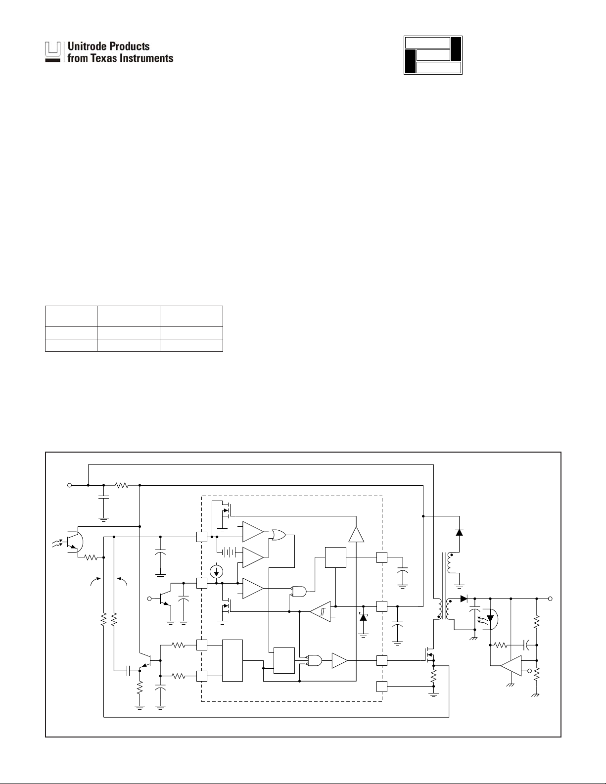
TYPICAL APPLICATION DIAGRAM
R
V
IN
FEEDBACK
CURRENT
SENSE
START
SLOPE
COMP
DISABLE
NOISE
FILTER
C
T
RT1
RT2
FB
1
+5V
SS
2
C
SS
3
4
1V
6µA
0.5V
OSC
1V
–
+
17.5V
REF
8
C
REF
V
–
+
V
REF
UDG-99036
OUT
VDD
7
C
VDD
OUT
6
GND
5
+
–
–
+
CLK
PWM
LATC H
R
S
5V
REF
–
15/8V
+
10/8V
UVLO
Q
SLUS166B - NOVEMBER 1999 - REVISED NOVEMBER 2004
ABSOLUTE MAXIMUM RATINGS*
VDD...........................................19V
I
..........................................25mA
VDD
I
(tpw < 1µs and Duty Cycle < 10%)........–0.4A to 0.8A
OUT
RT1, RT2, SS ......................–0.3V to REF + 0.3V
I
.........................................–15mA
REF
Storage Temperature ...................–65°C to +150°C
Junction Temperature...................–55°C to +150°C
Lead Temperature (Soldering, 10 sec.) .............+300°C
* Values beyond which damage may occur.
All voltages are with respect to ground unless otherwise stated.
Currents are positive into, negative out of the specified termi
nal. Consult Packaging Section of Databook for thermal limita
tions and considerations of packages.
UCC1809-1/-2
UCC2809-1/-2
UCC3809-1/-2
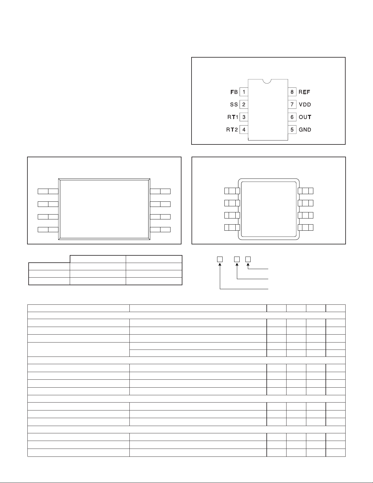
CONNECTION DIAGRAM
SOIC-8, DIL-8 (Top View)
D, N and J Packages
-
-
TSSOP-8 (Top View)
PW Package
FB
1
SS
2
RT1
3
RT2
4
REF
VDD
OUT
GND
8
7
6
5
MSOP-8 (Top View)
P Package
1
FB
2
SS
3
RT1
4
RT2
REF
VDD
OUT
GND
8
7
6
5
ORDERING INFORMATION
Temperature Range Available Packages
UCC1809-X –55°C to +125°C J
UCC2809-X –40°C to +85°C N, D, P, PW
UCC3809-X 0°C to +70°C N, D, P, PW
ELECTRICAL CHARACTERISTICS: Unless otherwise specified, C
PARAMETER TEST CONDITIONS MIN TYP MAX UNIT
Supply Section
VDD Clamp I
I
VDD
Starting (Note 1) 110 µA
I
VDD
Standby UCCx809-1, VDD = Start Threshold - 300mV 110 125 µA
I
VDD
Undervoltage Lockout Section
Start Threshold (UCCx809-1) 9.4 10.4 V
UVLO Hysteresis (UCCx809-1) 1.65 V
Start Threshold (UCCx809-2) 14.0 15.6 V
UVLO Hysteresis (UCCx809-2) 6.2 V
Voltage Reference Section
Output Voltage I
Line Regulation VDD = 10V to 15V 2 mV
Load Regulation I
Comparator Section
I
FB
Comparator Threshold 0.9 0.95 1 V
OUT Propagation Delay (No Load) V
= 10mA 16 17.5 19 V
VDD
No Load 600 900 µA
UCCx809-2, VDD = Start Threshold - 300mV 130 170 µA
= 0mA 4.75 5 5.25 V
REF
= 0mA to 5mA 2 mV
REF
Output Off –100 nA
= 0.8V to 1.2V at TR= 10ns 50 100 ns
FB
UCC 809 –
= 0.47 mF, VDD = 12V. TA=TJ.
VREF
UVLO OPTION
PACKAGE
TEMPERATURE RANGE
2

UCC1809-1/-2
UCC2809-1/-2
UCC3809-1/-2
ELECTRICAL CHARACTERISTICS: Unless otherwise specified, C
PARAMETER TEST CONDITIONS MIN TYP MAX UNIT
Soft Start Section
I
SS
Low VDD = 7.5V, ISS = 200mA 0.2 V
V
SS
Shutdown Threshold 0.44 0.48 0.52 V
Oscillator Section
Frequency RT1 = 10k, RT2 = 4.32k, CT = 820pF 90 100 110 kHz
Frequency Change with Voltage VDD = 10V to 15V 0.1 %/V
Peak Voltage 3.33 V
C
T
Valley Voltage 1.67 V
C
T
Peak to Peak Voltage 1.54 1.67 1.80 V
C
T
Output Section
Output V
Output V
Output Low Voltage During UVLO I
Minimum Duty Cycle V
Maximum Duty Cycle 70 %
Rise Time C
Fall Time C
Note 1. Ensured by design. Not 100% production tested.
Low I
SAT
High I
SAT
VDD = 16V, VSS = 0V; –40°Cto+85°C –4.9 –7.0 –9.1 mA
VDD = 16V, V
= 80mA (dc) 0.8 1.5 V
OUT
= –40mA (dc), VDD – OUT 0.8 1.5 V
OUT
= 20mA (dc) 1.5 V
OUT
=2V 0 %
FB
= 1nF 35 ns
OUT
= 1nF 18 ns
OUT
SS = 0V; < –40°C; >+85°C –4.0 –7.0 –10.0 mA
= 0.47 mF, VDD = 12V. TA=TJ.
VREF
PIN DESCRIPTIONS
FB: This pin is the summing node for current sense
feedback, voltage sense feedback (by optocoupler) and
slope compensation. Slope compensation is derived
from the rising voltage at the timing capacitor and can be
buffered with an external small signal NPN transistor.
External high frequency filter capacitance applied from
this node to GND is discharged by an internal 250W on
resistance NMOS FET during PWM off time and offers
effective leading edge blanking set by the RC time
constant of the feedback resistance from current sense
resistor to FB input and the high frequency filter capacitor
capacitance at this node to GND.
GND: Reference ground and power ground for all
functions.
OUT: This pin is the high current power driver output. A
minimum series gate resistor of 3.9W is recommended to
limit the gate drive current when operating with high bias
voltages.
REF: The internal 5V reference output. This reference is
buffered and is available on the REF pin. REF should be
bypassed with a 0.47mF ceramic capacitor.
RT2: This pin connects to timing resistor RT2 and
controls the negative ramp time of the internal oscillator
(Tf = 0.74 · (C
+ 27pF) · RT2). The negative threshold
T
of the internal oscillator is sensed through inactive timing
resistor RT1 which connects to pin RT1 and timing
capacitor C
.
T
SS: This pin serves two functions. The soft start timing
capacitor connects to SS and is charged by an internal
6µA current source. Under normal soft start SS is
discharged to at least 0.4V and then ramps positive to 1V
during which time the output driver is held low. As SS
charges from 1V to 2V soft start is implemented by an
increasing output duty cycle. If SS is taken below 0.5V,
the output driver is inhibited and held low. The user
accessible 5V voltage reference also goes low and I
VDD
< 100mA.
VDD: The power input connection for this device. This
pin is shunt regulated at 17.5V which is sufficiently below
the voltage rating of the DMOS output driver stage. VDD
should be bypassed with a 1mF ceramic capacitor.
RT1: This pin connects to timing resistor RT1 and
controls the positive ramp time of the internal oscillator
(Tr = 0.74 · (C
+ 27pF) · RT1). The positive threshold of
T
the internal oscillator is sensed through inactive timing
resistor RT2 which connects to pin RT2 and timing
capacitor C
.
T
3
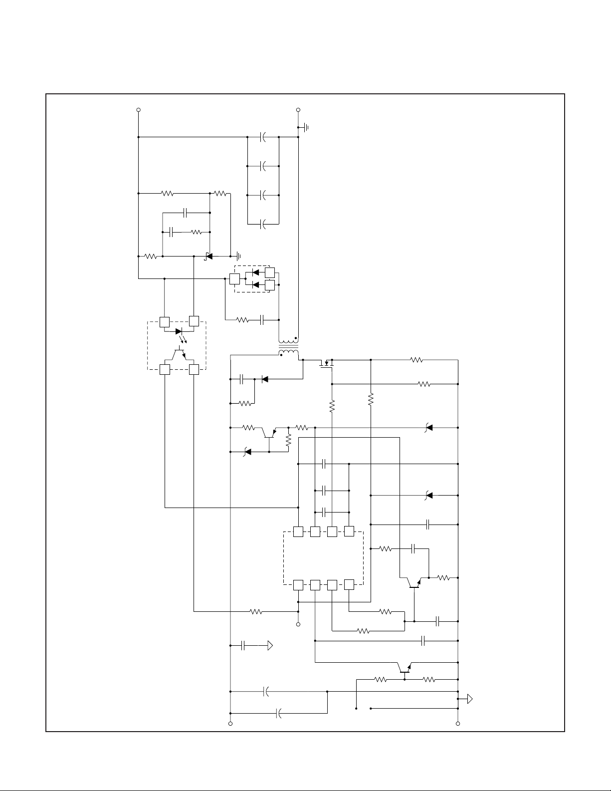
APPLICATION INFORMATION
UCC1809-1/-2
UCC2809-1/-2
UCC3809-1/-2
OUT
+V
C19
C18
1%
R17
12.1K
C14
470pF
C13
0.1µ F
R15
750
R14
2
1
H11AV1
4
5
U4
10K
U3
TL431
1%
R16
12.1K
C17
C16
U2
MBR2535CTL
2
3W
R19
5.1K
C10
D3
0.22 µF
2K
R9
3W
R13
1.1K
OUT
–V
6.3V
330 µF
6.3V
330 µF
6.3V
330 µF
6.3V
330 µF
3
1
µF
C15
0.015
T1
SF24
Q2
80µH
2N2907A
5:1
Q3
IRF640
1K
10
R10
680
R11
R6
R8
3W
0.15
R7
15K
D2
1N5245
+VIN
D4
R5
C3
1µF
1N5240
470
C2
PGND1
150 µF
C1
27K
R12
UCC3809
150 µF
C7
0.47 µF
C9
0.1µ F
C8
1µF
8
7
REF
VDD
FB
SS
2
1
TP1
6
OUT
RT1
3
5
GND
RT2
4
U1
R3
12.1K
ON/OFF
R20
5.62K
R4
6.19K
R1
5.1k
D1
5231B
C6
330pF
C22
0.1µ F
Q4
R18
3.01K
2N2222A
C5
1nF
C4
0.01 µF
Q1
2N2222A
R2
1.1K
PGND1
–VIN
UDG-99179
Figure 1. Isolated 50W flyback converter utilizing the UCC3809. The switching frequency is 70kHz, Vin = -32V to
-72V, Vout = +5V, Iout = 0A to 10A
4
APPLICATION INFORMATION (cont.)
K
The Typical Application Diagram shows an isolated
flyback converter utilizing the UCC3809. Note that the
capacitors C
REF
and C
tors for the reference and IC input voltage, respectively.
Both capacitors should be low ESR and ESL ceramic,
placed as close to the IC pins as possible, and returned
directly to the ground pin of the chip for best stability.
REF provides the internal bias to many of the IC func
tions and C
should be at least 0.47µF to prevent REF
REF
from drooping.
FB Pin
The basic premise of the UCC3809 is that the voltage
sense feedback signal originates from an optocoupler
that is modulated by an external error amplifier located
on the secondary side. This signal is summed with the
current sense signal and any slope compensation at the
FB pin and compared to a 1V threshold, as shown in the
Typical Application Diagram. Crossing this 1V threshold
resets the PWM latch and modulates the output driver
on-time much like the current sense comparator used in
the UC3842. In the absence of a FB signal, the output
will follow the programmed maximum on-time of the oscillator.
When adding slope compensation, it is important to use
a small capacitor to AC couple the oscillator waveform
before summing this signal into the FB pin. By correctly
selecting the emitter resistor of the optocoupler, the voltage sense signal can force the FB node to exceed the
1V threshold when the output that is being compared ex
ceeds a desired level. Doing so drives the UCC3809 to
zero percent duty cycle.
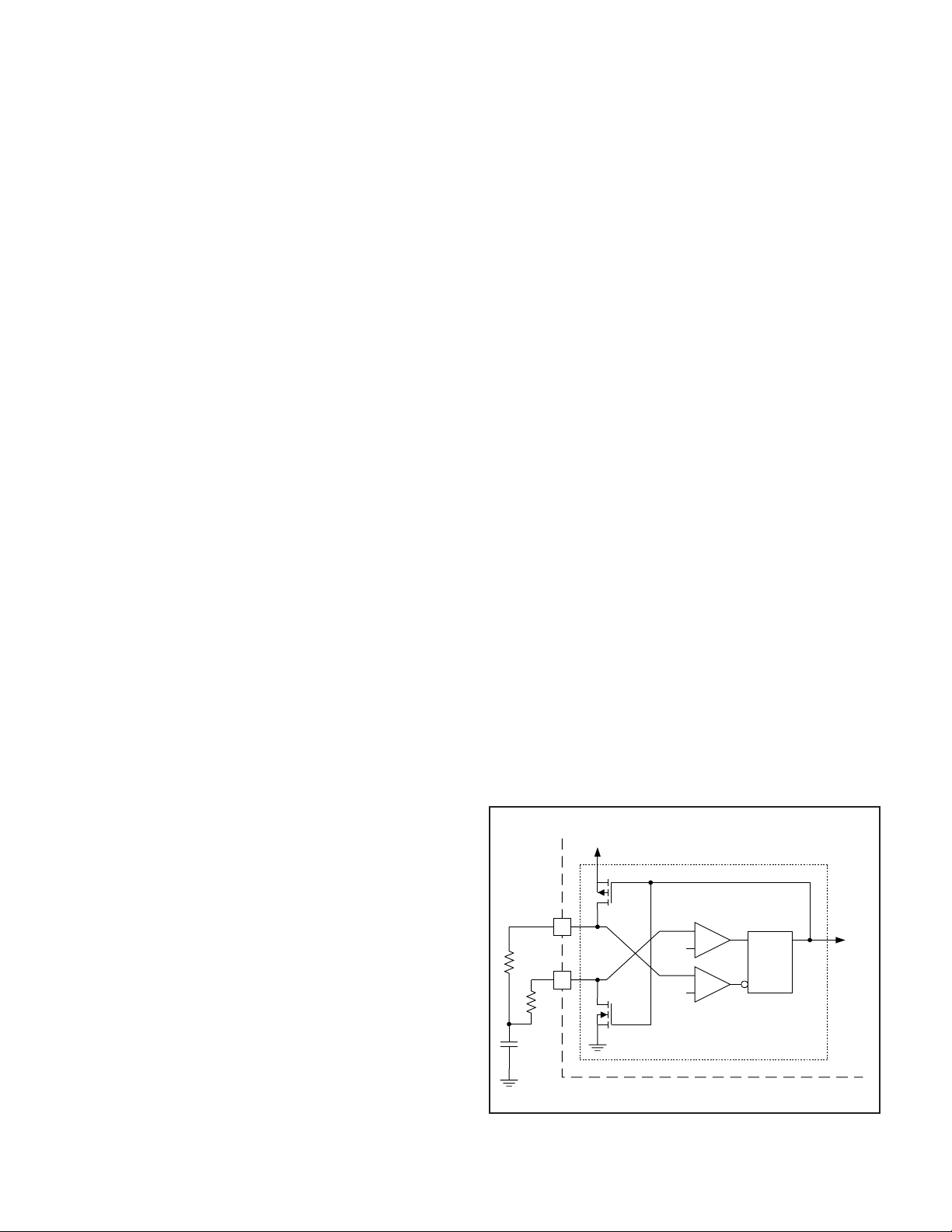
Oscillator
are local decoupling capaci
VDD
UCC1809-1/-2
UCC2809-1/-2
UCC3809-1/-2
reference) sensed through RT1. The R input to the oscil
lator latch, R(OSC), is also level sensitive and resets the
CLK signal low when CT crosses the 1.67V threshold,
turning off Q2 and turning on Q1, initiating another charg
ing cycle.
Figure 3 shows the waveforms associated with the oscil
lator latch and the PWM latch (shown in the Typical Ap
-
plication Diagram). A high CLK signal not only initiates a
discharge cycle for CT, it also turns on the internal NMOS
FET on the FB pin causing any external capacitance
used for leading edge blanking connected to this pin to
be discharged to ground. By discharging any external
capacitor completely to ground during the external
switch’s off-time, the noise immunity of the converter is
enhanced allowing the user to design in smaller RC com
ponents for leading edge blanking. A high CLK signal
also sets the level sensitive S input of the PWM latch,
S(PWM), high, resulting in a high output, Q(PWM), as
shown in Figure 3. This Q(PWM) signal will remain high
until a reset signal, R(PWM) is received. A high R(PWM)
signal results from the FB signal crossing the 1V threshold, or during soft start or if the SS pin is disabled.
Assuming the UVLO threshold is satisfied, the OUT signal of the IC will be high as long as Q(PWM) is high and
S(PWM), also referred to as CLK, is low. The OUT signal will be dominated by the FB signal as long as the FB
signal trips the 1V threshold while CLK is low. If the FB
signal does not cross the 1V threshold while CLK is low,
the OUT signal will be dominated by the maximum duty
cycle programmed by the user. Figure 3 illustrates the
various waveforms for a design set up for a maximum
duty cycle of 70%.
-
-
-
-
-
The following equation sets the oscillator frequency:
−
[]FCTpFRTRT
=•+ •+
OS C
DRTCTpFF
=•• + •074 1 27.
MAX OS C
()
074 27 1 2
.
()
()
1
Referring to Figure 2 and the waveforms in Figure 3,
when Q1is on, CT charges via the R
DS(on)
of Q1 and
RT1. During this charging process, the voltage of CT is
sensed through RT2. The S input of the oscillator latch,
S(OSC), is level sensitive, so crossing the upper thresh
old (set at 2/3 VREF or 3.33V for a typical 5.0V refer
ence) sets the Q output (CLK signal) of the oscillator
latch high. A high CLK signal results in turning off Q1 and
turning on Q2. CT now discharges through RT2 and the
R
DS(on)
of Q2. CT discharges from 3.33V to the lower
threshold (set at 1/3 VREF or 1.67V for a typical 5.0V
V
REF
Q1
3
RT1
4
-
CT
RT2
Q2
-
Figure 2. UCC3809 oscillator.
5
3.33V
1.67V
+
–
+
–
OSC
SQ
R
OS CILLAT OR
LATC H
CL
UDG-97195
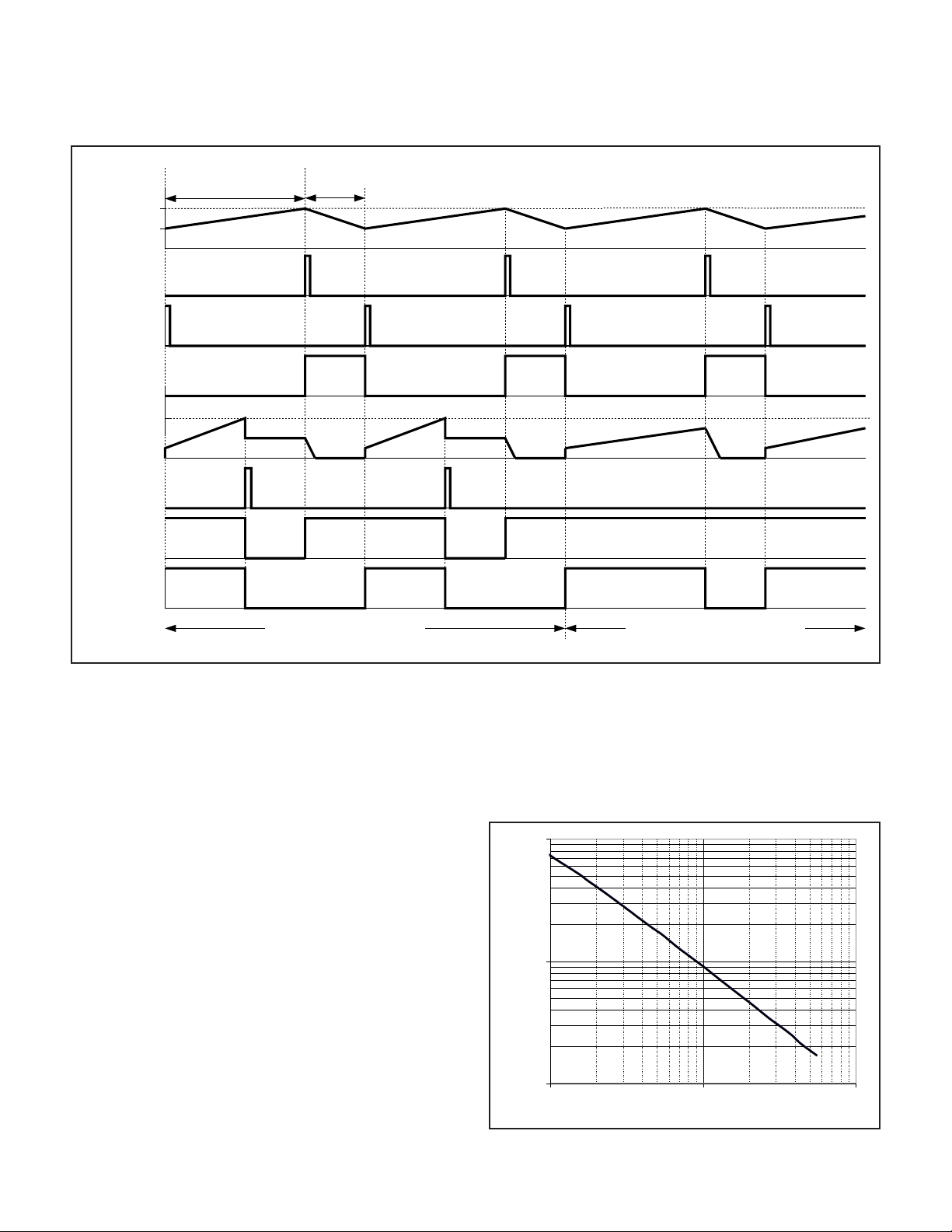
APPLICATION INFORMATION (cont.)
CT
CHARGINGCTDISCHARG ING
3.33V
1.67V
CT
S(OSC)
R(OSC)
Q(OSC)=CLK
=S(P WM)
1V
FB
R(PWM)
UCC1809-1/-2
UCC2809-1/-2
UCC3809-1/-2
Q(PWM)
OUT
FB S IG NAL DO MINAN T MAX. D UT Y CYCLE D O MINANT
Figure 3. Waveforms associated with the oscillator latch and the PWM latch.
The recommended value for CT is 1nF for frequencies in
the 100 kHz or less range and smaller CT for higher fre
-
1000
quencies. The minimum recommended values of RT1
and RT2 are 10kΩ and 4.32kΩ, respectively. Using these
values maintains a ratio of at least 20:1 between the
R
of the internal FETs and the external timing resis
DS(on)
tors, resulting in minimal change in frequency over tem
perature. Because of the oscillator's susceptibility to
-
-
100
capacitive coupling, examine the oscillator frequency by
looking at the common RT1-RT2-CT node on the circuit
FREQUENCY [kHz]
board as opposed to looking at pins 3 and 4 directly. For
good noise immunity, RT1 and RT2 should be placed as
close to pins 3 and 4 of the IC as possible. CT should be
returned directly to the ground pin of the IC with minimal
stray inductance and capacitance.
10
100 1000 10000
Figure 4. Oscillator frequency vs. CT(RT1 = 10k,
RT2 = 4.32k)
6
70%
ON
30%
OFF
UDG-99037
CT [pF]

APPLICATION INFORMATION (cont.)
Synchronization
UCC1809-1/-2
UCC2809-1/-2
UCC3809-1/-2
changed.
Both of the synchronization schemes shown in Figure 5
can be successfully implemented with the internal oscilla
tor of the UCC3809. Both schemes allow access to the
timing ramp needed for slope compensation and have
minimal impact on the programmed maximum duty cycle.
In the absence of a sync pulse, the PWM controller will
run independently at the frequency set by RT1, RT2, and
CT. This free running frequency must be approximately
15 to 20% lower than the sync pulse frequency to insure
the free running oscillator does not cross the comparator
threshold before the desired sync pulse.
Option I uses the synchronization pulse to pull pin 3 low,
triggering the internal 1.67V comparator to reset the RS
latch and initiate a charging cycle. The valley voltage of
the CT waveform is higher when synchronized using this
configuration, decreasing the ramp charge and discharge
times, thereby increasing the operating frequency; otherwise the overall shape of the CT voltage waveform is un-
Option II uses the synchronization pulse to superimpose
-
the sync voltage onto the peak of the CT waveform. This
triggers the internal 3.33V comparator, initiating a dis
charge cycle. The sync pulse is summed with the free
running oscillator waveform at the CT node, resulting in a
spike on top of the CT peak voltage.
ADDITIONAL INFORMATION
Please refer to the following Unitrode application topics
for additional information.
[1] Application Note U-165, Design Review: Isolated 50W
Flyback Converter with the UCC3809 Primary Side Con
troller by Lisa Dinwoodie.
[2] Design Note DN-89, Comparing the UC3842,
UCC3802, and UCC3809 Primary Side PWM Controllers
by Lisa Dinwoodie.
-
-
1k
3
SYNC
PULSE
2N2222A
424
RT1
4
RT2
CT
OPTION I
Figure 5. UCC3809 synchronization options.
UCC3809
OS C ILLATO R
+5V
SYNC
PULSE
2N2222A
0.1µF
424
RT1
RT2
CT
24
OPTION II
3
UCC3809
OS C ILLATO R
4
UDG-99006
7

TYPICAL CHARACTERISTICS CURVES
UCC1809-1/-2
UCC2809-1/-2
UCC3809-1/-2
180
160
140
120
100
80
60
Idd standby (uA)
40
20
0
-50 -25 0 25 50 75 100 125
Temperature (deg C)
UCC2809-2
UCC2809-1
Figure 6. IDD(standby) vs. temperature.
110
105
16
14
12
10
8
UVLO (V)
6
4
2
0
-50 -25 0 25 50 75 100 125
Temperature (deg C)
2809-2 UVLO on
2809-1UVLO on
UVLO off
Figure 7. UVLO vs. temperature.
100
95
Oscillator frequency (kHz)
90
-50 -25 0 25 50 75 100 125
temperature (deg C)
Figure 8. Oscillator frequency vs. temperature.
REVISION HISTORY
REV. B 11/04
Added Ivdd Stand-by Current specifications in the Electrical Characteristics table.
Modified Ivdd Starting specifications in the Electrical Characteristics table.
Added Typical Characteristics Curves for Idd(Standby), UVLO thresholds, and Oscillator Frequency.
8

PACKAGE OPTION ADDENDUM
www.ti.com
PACKAGING INFORMATION
Orderable Device Status
UCC2809D-1 ACTIVE SOIC D 8 75 Green (RoHS &
UCC2809D-1G4 ACTIVE SOIC D 8 75 Green (RoHS &
UCC2809D-2 ACTIVE SOIC D 8 75 Green (RoHS &
UCC2809D-2G4 ACTIVE SOIC D 8 75 Green (RoHS &
UCC2809DTR-1 ACTIVE SOIC D 8 2500 Green (RoHS &
UCC2809DTR-1G4 ACTIVE SOIC D 8 2500 Green (RoHS &
UCC2809DTR-2 ACTIVE SOIC D 8 2500 Green (RoHS &
UCC2809DTR-2G4 ACTIVE SOIC D 8 2500 Green (RoHS &
UCC2809P-1 ACTIVE MSOP DGK 8 80 Green (RoHS &
UCC2809P-1G4 ACTIVE MSOP DGK 8 80 Green (RoHS &
UCC2809P-2 ACTIVE MSOP DGK 8 80 Green (RoHS &
UCC2809P-2G4 ACTIVE MSOP DGK 8 80 Green (RoHS &
UCC2809PTR-1 ACTIVE MSOP DGK 8 2500 Green (RoHS &
UCC2809PTR-1G4 ACTIVE MSOP DGK 8 2500 Green (RoHS &
UCC2809PTR-2 ACTIVE MSOP DGK 8 2500 Green (RoHS &
UCC2809PTR-2G4 ACTIVE MSOP DGK 8 2500 Green (RoHS &
UCC2809PW-1 ACTIVE TSSOP PW 8 150 Green (RoHS &
UCC2809PW-1G4 ACTIVE TSSOP PW 8 150 Green (RoHS &
UCC2809PW-2 ACTIVE TSSOP PW 8 150 Green (RoHS &
UCC2809PW-2G4 ACTIVE TSSOP PW 8 150 Green (RoHS &
UCC2809PWTR-1 ACTIVE TSSOP PW 8 2000 Green (RoHS &
UCC2809PWTR-1G4 ACTIVE TSSOP PW 8 2000 Green (RoHS &
UCC2809PWTR-2G4 ACTIVE TSSOP PW 8 TBD Call TI Call TI
UCC3809D-1 ACTIVE SOIC D 8 75 Green (RoHS &
UCC3809D-1G4 ACTIVE SOIC D 8 75 Green (RoHS &
(1)
Package
Type
Package
Drawing
Pins Package
Qty
Eco Plan
no Sb/Br)
no Sb/Br)
no Sb/Br)
no Sb/Br)
no Sb/Br)
no Sb/Br)
no Sb/Br)
no Sb/Br)
no Sb/Br)
no Sb/Br)
no Sb/Br)
no Sb/Br)
no Sb/Br)
no Sb/Br)
no Sb/Br)
no Sb/Br)
no Sb/Br)
no Sb/Br)
no Sb/Br)
no Sb/Br)
no Sb/Br)
no Sb/Br)
no Sb/Br)
no Sb/Br)
(2)
Lead/Ball Finish MSL Peak Temp
CU NIPDAU Level-1-260C-UNLIM
CU NIPDAU Level-1-260C-UNLIM
CU NIPDAU Level-1-260C-UNLIM
CU NIPDAU Level-1-260C-UNLIM
CU NIPDAU Level-1-260C-UNLIM
CU NIPDAU Level-1-260C-UNLIM
CU NIPDAU Level-1-260C-UNLIM
CU NIPDAU Level-1-260C-UNLIM
CU NIPDAU Level-2-260C-1 YEAR
CU NIPDAU Level-2-260C-1 YEAR
CU NIPDAU Level-2-260C-1 YEAR
CU NIPDAU Level-2-260C-1 YEAR
CU NIPDAU Level-2-260C-1 YEAR
CU NIPDAU Level-2-260C-1 YEAR
CU NIPDAU Level-2-260C-1 YEAR
CU NIPDAU Level-2-260C-1 YEAR
CU NIPDAU Level-2-260C-1 YEAR
CU NIPDAU Level-2-260C-1 YEAR
CU NIPDAU Level-2-260C-1 YEAR
CU NIPDAU Level-2-260C-1 YEAR
CU NIPDAU Level-2-260C-1 YEAR
CU NIPDAU Level-2-260C-1 YEAR
CU NIPDAU Level-1-260C-UNLIM
CU NIPDAU Level-1-260C-UNLIM
3-Mar-2008
(3)
Addendum-Page 1

PACKAGE OPTION ADDENDUM
www.ti.com
Orderable Device Status
(1)
Package
Type
Package
Drawing
Pins Package
Qty
Eco Plan
(2)
UCC3809D-2 ACTIVE SOIC D 8 75 Green (RoHS &
no Sb/Br)
UCC3809D-2G4 ACTIVE SOIC D 8 75 Green (RoHS &
no Sb/Br)
UCC3809DTR-1 ACTIVE SOIC D 8 2500 Green (RoHS &
no Sb/Br)
UCC3809DTR-1G4 ACTIVE SOIC D 8 2500 Green (RoHS &
no Sb/Br)
UCC3809DTR-2 ACTIVE SOIC D 8 2500 Green (RoHS &
no Sb/Br)
UCC3809DTR-2G4 ACTIVE SOIC D 8 2500 Green (RoHS &
no Sb/Br)
UCC3809N-1 ACTIVE PDIP P 8 50 Green (RoHS &
no Sb/Br)
UCC3809N-1G4 ACTIVE PDIP P 8 50 Green (RoHS &
no Sb/Br)
UCC3809N-2 ACTIVE PDIP P 8 50 Green (RoHS &
no Sb/Br)
UCC3809N-2G4 ACTIVE PDIP P 8 50 Green (RoHS &
no Sb/Br)
UCC3809P-1 ACTIVE MSOP DGK 8 80 Green (RoHS &
no Sb/Br)
UCC3809P-1G4 ACTIVE MSOP DGK 8 80 Green (RoHS &
no Sb/Br)
UCC3809P-2 ACTIVE MSOP DGK 8 80 Green (RoHS &
no Sb/Br)
UCC3809P-2G4 ACTIVE MSOP DGK 8 80 Green (RoHS &
no Sb/Br)
UCC3809PTR-1 ACTIVE MSOP DGK 8 2500 Green (RoHS &
no Sb/Br)
UCC3809PTR-1G4 ACTIVE MSOP DGK 8 2500 Green (RoHS &
no Sb/Br)
UCC3809PTR-2 ACTIVE MSOP DGK 8 2500 Green (RoHS &
no Sb/Br)
UCC3809PTR-2G4 ACTIVE MSOP DGK 8 2500 Green (RoHS &
no Sb/Br)
UCC3809PW-1 ACTIVE TSSOP PW 8 150 Green (RoHS &
no Sb/Br)
UCC3809PW-1G4 ACTIVE TSSOP PW 8 150 Green (RoHS &
no Sb/Br)
UCC3809PW-2 ACTIVE TSSOP PW 8 150 Green (RoHS &
no Sb/Br)
UCC3809PW-2G4 ACTIVE TSSOP PW 8 150 Green (RoHS &
no Sb/Br)
UCC3809PWTR-1 ACTIVE TSSOP PW 8 2000 Green (RoHS &
no Sb/Br)
UCC3809PWTR-1G4 ACTIVE TSSOP PW 8 2000 Green (RoHS &
no Sb/Br)
(1)
The marketing status values are defined as follows:
ACTIVE: Product device recommended for new designs.
LIFEBUY: TI has announced that the device will be discontinued, and a lifetime-buy period is in effect.
3-Mar-2008
Lead/Ball Finish MSL Peak Temp
CU NIPDAU Level-1-260C-UNLIM
CU NIPDAU Level-1-260C-UNLIM
CU NIPDAU Level-1-260C-UNLIM
CU NIPDAU Level-1-260C-UNLIM
CU NIPDAU Level-1-260C-UNLIM
CU NIPDAU Level-1-260C-UNLIM
CU NIPDAU N / A for Pkg Type
CU NIPDAU N / A for Pkg Type
CU NIPDAU N / A for Pkg Type
CU NIPDAU N / A for Pkg Type
CU NIPDAU Level-2-260C-1 YEAR
CU NIPDAU Level-2-260C-1 YEAR
CU NIPDAU Level-2-260C-1 YEAR
CU NIPDAU Level-2-260C-1 YEAR
CU NIPDAU Level-2-260C-1 YEAR
CU NIPDAU Level-2-260C-1 YEAR
CU NIPDAU Level-2-260C-1 YEAR
CU NIPDAU Level-2-260C-1 YEAR
CU NIPDAU Level-2-260C-1 YEAR
CU NIPDAU Level-2-260C-1 YEAR
CU NIPDAU Level-2-260C-1 YEAR
CU NIPDAU Level-2-260C-1 YEAR
CU NIPDAU Level-2-260C-1 YEAR
CU NIPDAU Level-2-260C-1 YEAR
(3)
Addendum-Page 2

PACKAGE OPTION ADDENDUM
www.ti.com
NRND: Not recommended for new designs. Device is in production to support existing customers, but TI does not recommend using this part in
a new design.
PREVIEW: Device has been announced but is not in production. Samples may or may not be available.
OBSOLETE: TI has discontinued the production of the device.
(2)
Eco Plan - The planned eco-friendly classification: Pb-Free (RoHS), Pb-Free (RoHS Exempt), or Green (RoHS & no Sb/Br) - please check
http://www.ti.com/productcontent for the latest availability information and additional product content details.
TBD: The Pb-Free/Green conversion plan has not been defined.
Pb-Free (RoHS): TI's terms "Lead-Free" or "Pb-Free" mean semiconductor products that are compatible with the current RoHS requirements
for all 6 substances, including the requirement that lead not exceed 0.1% by weight in homogeneous materials. Where designed to be soldered
at high temperatures, TI Pb-Free products are suitable for use in specified lead-free processes.
Pb-Free (RoHS Exempt): This component has a RoHS exemption for either 1) lead-based flip-chip solder bumps used between the die and
package, or 2) lead-based die adhesive used between the die and leadframe. The component is otherwise considered Pb-Free (RoHS
compatible) as defined above.
Green (RoHS & no Sb/Br): TI defines "Green" to mean Pb-Free (RoHS compatible), and free of Bromine (Br) and Antimony (Sb) based flame
retardants (Br or Sb do not exceed 0.1% by weight in homogeneous material)
(3)
MSL, Peak Temp. -- The Moisture Sensitivity Level rating according to the JEDEC industry standard classifications, and peak solder
temperature.
Important Information and Disclaimer:The information provided on this page represents TI's knowledge and belief as of the date that it is
provided. TI bases its knowledge and belief on information provided by third parties, and makes no representation or warranty as to the
accuracy of such information. Efforts are underway to better integrate information from third parties. TI has taken and continues to take
reasonable steps to provide representative and accurate information but may not have conducted destructive testing or chemical analysis on
incoming materials and chemicals. TI and TI suppliers consider certain information to be proprietary, and thus CAS numbers and other limited
information may not be available for release.
3-Mar-2008
In no event shall TI's liability arising out of such information exceed the total purchase price of the TI part(s) at issue in this document sold by TI
to Customer on an annual basis.
Addendum-Page 3

PACKAGE MATERIALS INFORMATION
www.ti.com
TAPE AND REEL INFORMATION
19-Mar-2008
*All dimensions are nominal
Device Package
Type
UCC2809DTR-1 SOIC D 8 2500 330.0 12.4 6.4 5.2 2.1 8.0 12.0 Q1
UCC2809DTR-1 SOIC D 8 2500 330.0 12.4 6.4 5.2 2.1 8.0 12.0 Q1
UCC2809DTR-2 SOIC D 8 2500 330.0 12.4 6.4 5.2 2.1 8.0 12.0 Q1
UCC2809DTR-2 SOIC D 8 2500 330.0 12.4 6.4 5.2 2.1 8.0 12.0 Q1
UCC2809PTR-1 MSOP DGK 8 2500 330.0 12.4 5.3 3.4 1.4 8.0 12.0 Q1
UCC2809PTR-2 MSOP DGK 8 2500 330.0 12.4 5.3 3.4 1.4 8.0 12.0 Q1
UCC2809PWTR-1 TSSOP PW 8 2000 330.0 12.4 7.0 3.6 1.6 8.0 12.0 Q1
UCC3809DTR-1 SOIC D 8 2500 330.0 12.4 6.4 5.2 2.1 8.0 12.0 Q1
UCC3809DTR-1 SOIC D 8 2500 330.0 12.4 6.4 5.2 2.1 8.0 12.0 Q1
UCC3809DTR-2 SOIC D 8 2500 330.0 12.4 6.4 5.2 2.1 8.0 12.0 Q1
UCC3809DTR-2 SOIC D 8 2500 330.0 12.4 6.4 5.2 2.1 8.0 12.0 Q1
UCC3809PTR-1 MSOP DGK 8 2500 330.0 12.4 5.3 3.4 1.4 8.0 12.0 Q1
UCC3809PTR-2 MSOP DGK 8 2500 330.0 12.4 5.3 3.4 1.4 8.0 12.0 Q1
UCC3809PWTR-1 TSSOP PW 8 2000 330.0 12.4 7.0 3.6 1.6 8.0 12.0 Q1
Package
Drawing
Pins SPQ Reel
Diameter
(mm)
Reel
Width
W1 (mm)
A0 (mm) B0 (mm) K0 (mm) P1
(mm)W(mm)
Pin1
Quadrant
Pack Materials-Page 1

PACKAGE MATERIALS INFORMATION
www.ti.com
19-Mar-2008
*All dimensions are nominal
Device Package Type Package Drawing Pins SPQ Length (mm) Width (mm) Height (mm)
UCC2809DTR-1 SOIC D 8 2500 346.0 346.0 29.0
UCC2809DTR-1 SOIC D 8 2500 340.5 338.1 20.6
UCC2809DTR-2 SOIC D 8 2500 340.5 338.1 20.6
UCC2809DTR-2 SOIC D 8 2500 346.0 346.0 29.0
UCC2809PTR-1 MSOP DGK 8 2500 346.0 346.0 29.0
UCC2809PTR-2 MSOP DGK 8 2500 346.0 346.0 29.0
UCC2809PWTR-1 TSSOP PW 8 2000 346.0 346.0 29.0
UCC3809DTR-1 SOIC D 8 2500 340.5 338.1 20.6
UCC3809DTR-1 SOIC D 8 2500 346.0 346.0 29.0
UCC3809DTR-2 SOIC D 8 2500 340.5 338.1 20.6
UCC3809DTR-2 SOIC D 8 2500 346.0 346.0 29.0
UCC3809PTR-1 MSOP DGK 8 2500 346.0 346.0 29.0
UCC3809PTR-2 MSOP DGK 8 2500 346.0 346.0 29.0
UCC3809PWTR-1 TSSOP PW 8 2000 346.0 346.0 29.0
Pack Materials-Page 2

MECHANICAL DATA
MTSS001C – JANUARY 1995 – REVISED FEBRUARY 1999
PW (R-PDSO-G**) PLASTIC SMALL-OUTLINE PACKAGE
14 PINS SHOWN
0,65
1,20 MAX
14
0,30
0,19
8
4,50
4,30
PINS **
7
Seating Plane
0,15
0,05
8
1
A
DIM
14
0,10
6,60
6,20
M
0,10
0,15 NOM
2016
0°–8°
Gage Plane
24
0,25
0,75
0,50
28
A MAX
A MIN
NOTES: A. All linear dimensions are in millimeters.
B. This drawing is subject to change without notice.
C. Body dimensions do not include mold flash or protrusion not to exceed 0,15.
D. Falls within JEDEC MO-153
3,10
2,90
5,10
4,90
5,10
4,90
6,60
6,40
7,90
7,70
9,80
9,60
4040064/F 01/97
POST OFFICE BOX 655303 • DALLAS, TEXAS 75265


MECHANICAL DATA
MPDI001A – JANUARY 1995 – REVISED JUNE 1999
P (R-PDIP-T8) PLASTIC DUAL-IN-LINE
0.400 (10,60)
0.355 (9,02)
8
5
0.260 (6,60)
0.240 (6,10)
1
0.021 (0,53)
0.015 (0,38)
NOTES: A. All linear dimensions are in inches (millimeters).
B. This drawing is subject to change without notice.
C. Falls within JEDEC MS-001
4
0.070 (1,78) MAX
0.020 (0,51) MIN
0.200 (5,08) MAX
0.125 (3,18) MIN
0.100 (2,54)
0.010 (0,25)
Seating Plane
M
0.325 (8,26)
0.300 (7,62)
0.015 (0,38)
Gage Plane
0.010 (0,25) NOM
0.430 (10,92)
MAX
4040082/D 05/98
For the latest package information, go to http://www.ti.com/sc/docs/package/pkg_info.htm
POST OFFICE BOX 655303 • DALLAS, TEXAS 75265

IMPORTANT NOTICE
Texas Instruments Incorporated and its subsidiaries (TI) reserve the right to make corrections, modifications, enhancements, improvements,
and other changes to its products and services at any time and to discontinue any product or service without notice. Customers should
obtain the latest relevant information before placing orders and should verify that such information is current and complete. All products are
sold subject to TI’s terms and conditions of sale supplied at the time of order acknowledgment.
TI warrants performance of its hardware products to the specifications applicable at the time of sale in accordance with TI’s standard
warranty. Testing and other quality control techniques are used to the extent TI deems necessary to support this warranty. Except where
mandated by government requirements, testing of all parameters of each product is not necessarily performed.
TI assumes no liability for applications assistance or customer product design. Customers are responsible for their products and
applications using TI components. To minimize the risks associated with customer products and applications, customers should provide
adequate design and operating safeguards.
TI does not warrant or represent that any license, either express or implied, is granted under any TI patent right, copyright, mask work right,
or other TI intellectual property right relating to any combination, machine, or process in which TI products or services are used. Information
published by TI regarding third-party products or services does not constitute a license from TI to use such products or services or a
warranty or endorsement thereof. Use of such information may require a license from a third party under the patents or other intellectual
property of the third party, or a license from TI under the patents or other intellectual property of TI.
Reproduction of TI information in TI data books or data sheets is permissible only if reproduction is without alteration and is accompanied
by all associated warranties, conditions, limitations, and notices. Reproduction of this information with alteration is an unfair and deceptive
business practice. TI is not responsible or liable for such altered documentation. Information of third parties may be subject to additional
restrictions.
Resale of TI products or services with statements different from or beyond the parameters stated by TI for that product or service voids all
express and any implied warranties for the associated TI product or service and is an unfair and deceptive business practice. TI is not
responsible or liable for any such statements.
TI products are not authorized for use in safety-critical applications (such as life support) where a failure of the TI product would reasonably
be expected to cause severe personal injury or death, unless officers of the parties have executed an agreement specifically governing
such use. Buyers represent that they have all necessary expertise in the safety and regulatory ramifications of their applications, and
acknowledge and agree that they are solely responsible for all legal, regulatory and safety-related requirements concerning their products
and any use of TI products in such safety-critical applications, notwithstanding any applications-related information or support that may be
provided by TI. Further, Buyers must fully indemnify TI and its representatives against any damages arising out of the use of TI products in
such safety-critical applications.
TI products are neither designed nor intended for use in military/aerospace applications or environments unless the TI products are
specifically designated by TI as military-grade or "enhanced plastic." Only products designated by TI as military-grade meet military
specifications. Buyers acknowledge and agree that any such use of TI products which TI has not designated as military-grade is solely at
the Buyer's risk, and that they are solely responsible for compliance with all legal and regulatory requirements in connection with such use.
TI products are neither designed nor intended for use in automotive applications or environments unless the specific TI products are
designated by TI as compliant with ISO/TS 16949 requirements. Buyers acknowledge and agree that, if they use any non-designated
products in automotive applications, TI will not be responsible for any failure to meet such requirements.
Following are URLs where you can obtain information on other Texas Instruments products and application solutions:
Products Applications
Amplifiers amplifier.ti.com Audio www.ti.com/audio
Data Converters dataconverter.ti.com Automotive www.ti.com/automotive
DSP dsp.ti.com Broadband www.ti.com/broadband
Clocks and Timers www.ti.com/clocks Digital Control www.ti.com/digitalcontrol
Interface interface.ti.com Medical www.ti.com/medical
Logic logic.ti.com Military www.ti.com/military
Power Mgmt power.ti.com Optical Networking www.ti.com/opticalnetwork
Microcontrollers microcontroller.ti.com Security www.ti.com/security
RFID www.ti-rfid.com Telephony www.ti.com/telephony
RF/IF and ZigBee® Solutions www.ti.com/lprf Video & Imaging www.ti.com/video
Mailing Address: Texas Instruments, Post Office Box 655303, Dallas, Texas 75265
Copyright © 2008, Texas Instruments Incorporated
Wireless www.ti.com/wireless
 Loading...