

Texas Instruments UC5602QPTR, UC5602QP, UC5602DWPTR, UC5602DWP Datasheet
UC5602
SCSI Active Terminator
FEATURES DESCRIPTION
• Complies with SCSI, SCSI-2
Standards
• 10pF Channel Capacitance During
Disconnect
• Active Termination for 18 Lines
• Logic Command Disconnects all
Termination Lines
• Low Supply Current in Disconnect
Mode
• Trimmed Regulator for Accurate
Termination Current
• Current Limit and Thermal
Shutdown Protection
• 110 Ohm Termination
• Meets SCSI Hot Plugging
The UC5602 is a pi n compatible version of its predecessor, the UC5601,
and is targeted for high vol ume applicatio ns which req uire ac tive termination, but not the high performance of the UC5601. The major differences
are relaxed outpu t current and termination tolerances, and the absence of
low side clamps.
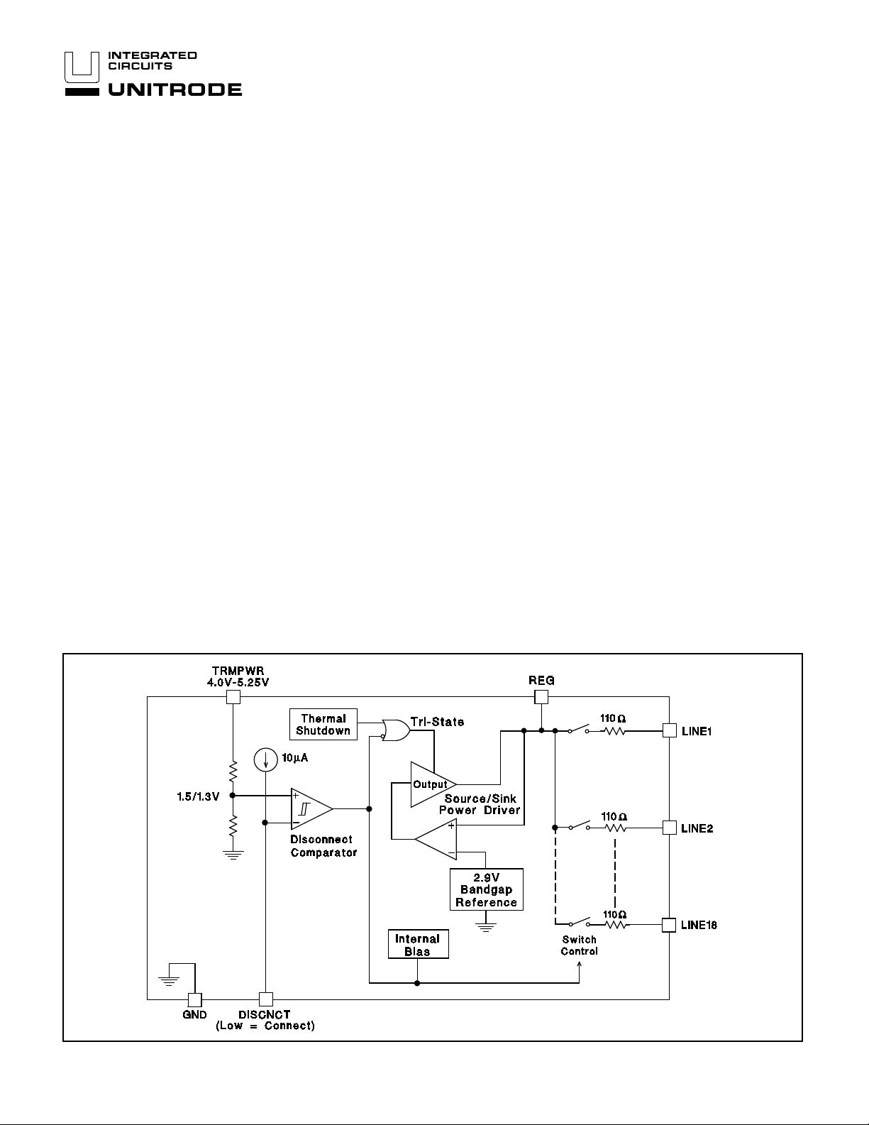
The UC5602 provides 18 lines of active termination for a SCSI (Small
Computer Systems Interface) paral lel bus. The SCSI-2 standard recommends active termination at both ends of the cable segment, and SCSI-3
will make it a requirement.
The UC5602 provides a disco nnect feature whi ch, when open ed or driven
high, will disconnect all termi nating resistors, and disables the regu lator;
greatly reduci ng standby powe r. The output channels remain high impedance even without Termpwr applied.
Internal circuit trimming is utilized, first to trim the impedance to a 7% tolerance; and then most importantly, to trim the output current 7% tolerance,
as close to the max SCSI as possible, which maximizes noise margin in
fast SCSI operation.
Other features include thermal shutdown, current limit, and 40mA of active
negation sink current capability.
BLOCK DIAGRAM
This device is offered in low thermal re sistance versions of the industry
standard 28 pin wide body SOIC and PLCC, as well as a 24 pin DIL plastic
package.
10/94
UDG-94052
Circuit Design Patented
UC5602
ABSOLUTE MAXIMUM RATINGS
Termpwr Voltage . . . . . . . . . . . . . . . . . . . . . . . . . . . . . . . . . +7V
Signal Line Voltage. . . . . . . . . . . . . . . . . . . . . . . . . . . 0V to +7V
Regulator Output Current. . . . . . . . . . . . . . . . . . . . . . . . . . 0.5A
Storage Temperature . . . . . . . . . . . . . . . . . . . −−65°C to +150°C
Operating Tem perat ure . . . . . . . . . . . . . . . . . −−55°C t o +150° C
Lead Temperat ure (Solde ring, 10 Sec.). . . . . . . . . . . . . +300°C
Unless otherwise specified all volta ges are with respect to
Ground. Cur ren ts are po sitive into, negative out of the specified terminal.
Consult Packaging Section of Unitr ode Int egr ated Circ uits databook for thermal limitations and consider ations of pack ages .
RECOMMENDED OPERATING CONDITIONS
Termpwr Voltage . . . . . . . . . . . . . . . . . . . . . . . . . 4.0V to 5.25V
Signal Line Voltage. . . . . . . . . . . . . . . . . . . . . . . . . . . 0V to +3V
Disconnect Input Voltage . . . . . . . . . . . . . . . . . . 0V to Termpwr
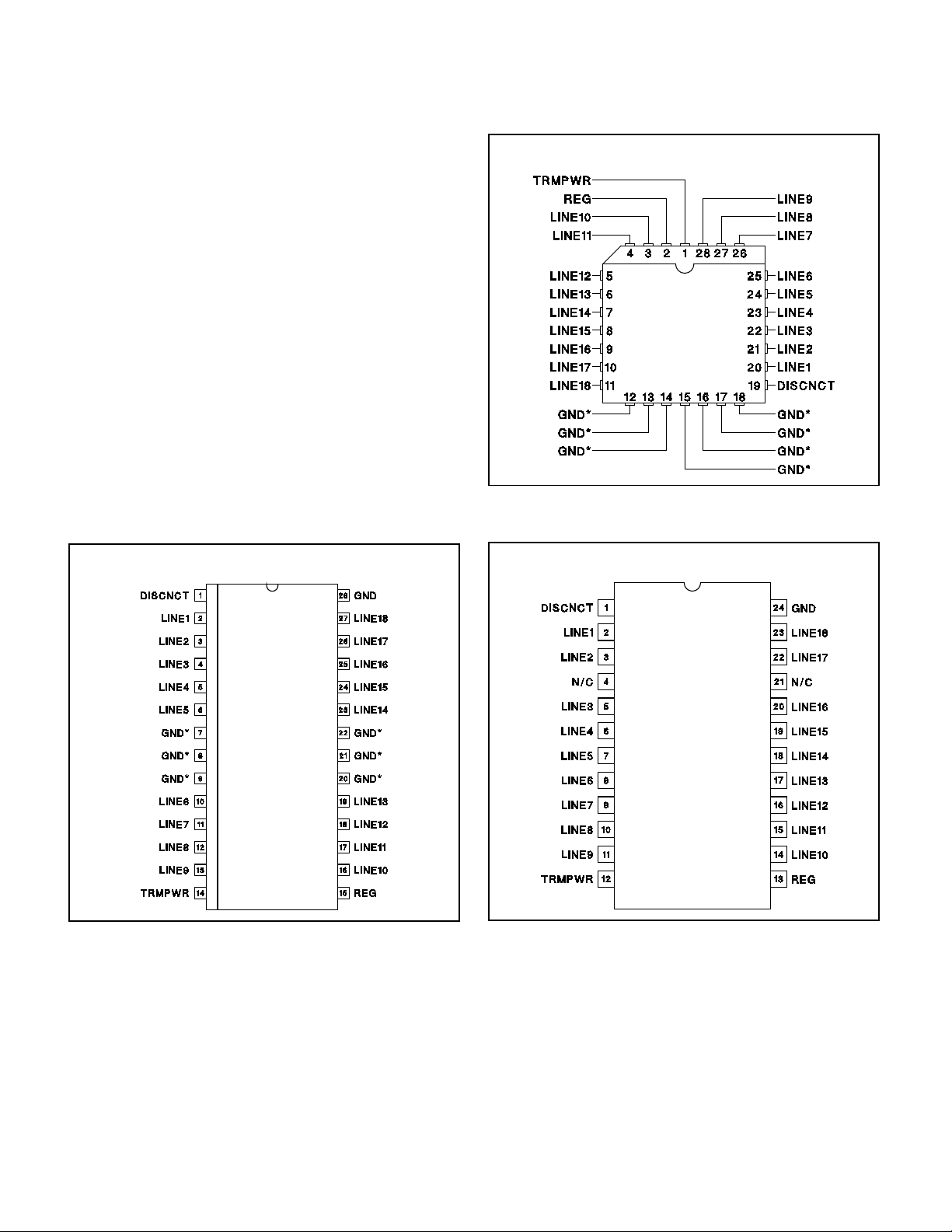
SOIC-28 (Top View)
DWP Package
CONNECTION DIAGRAMS
PLCC-28 (Top View)
QP Package
* QP package pins 12 - 18 serve as both hea tsink and sign al
ground.
DIL-24 (Top View)
N Package
* DWP package pin 28 serves as signal ground ; pins 7, 8, 9,
20, 21, 22 serve as heatsink/ground.
Note: Drawings are not to scale.
2
 Loading...