Texas Instruments UC5180CQTR, UC5180CQ, UC5180CN, UC5180CJ Datasheet

ABSOLUTE MAXIMUM RATINGS (Note 1)
Supply Voltage, VCC . . . . . . . . . . . . . . . . . . . . . . . . . . . . . . . . . . . . . . . . . . . 7V
Output Sink Current. . . . . . . . . . . . . . . . . . . . . . . . . . . . . . . . . . . . . . . . . 50 mA
Output Sho rt C ircuit Time . . . . . . . . . . . . . . . . . . . . . . . . . . . . . . . . . . . . . 1 Sec
Common Mo de Inpu t Ra nge. . . . . . . . . . . . . . . . . . . . . . . . . . . . . . . . . . . . 15V
Differential I nput Range. . . . . . . . . . . . . . . . . . . . . . . . . . . . . . . . . . . . . . . . 25V
Failsafe Voltage. . . . . . . . . . . . . . . . . . . . . . . . . . . . . . . . . . . . . . . . . -0.3 to V
CC
PLCC Power Dissipation, TA = 25°C (Note 2). . . . . . . . . . . . . . . . . . . 1000 mW
DIP Power Dissipation, T
A = 25°C (Note 2) . . . . . . . . . . . . . . . . . . . . 1200 mW
Storage Temp era ture Ran ge. . . . . . . . . . . . . . . . . . . . . . . . . . -65°C to +150°C
Lead Temperatur e (So ldering , 10 Second s). . . . . . . . . . . . . . . . . . . . . . -300°C
Note 1: All voltages are with respect to ground, pin 14. Curren ts are positive
into, negative out of the specif ied t erminal
Note 2: Consult Packa ging Section of Databo ok for ther mal limitations and
considerations of package.
Octal Line Receiver
UC5180C
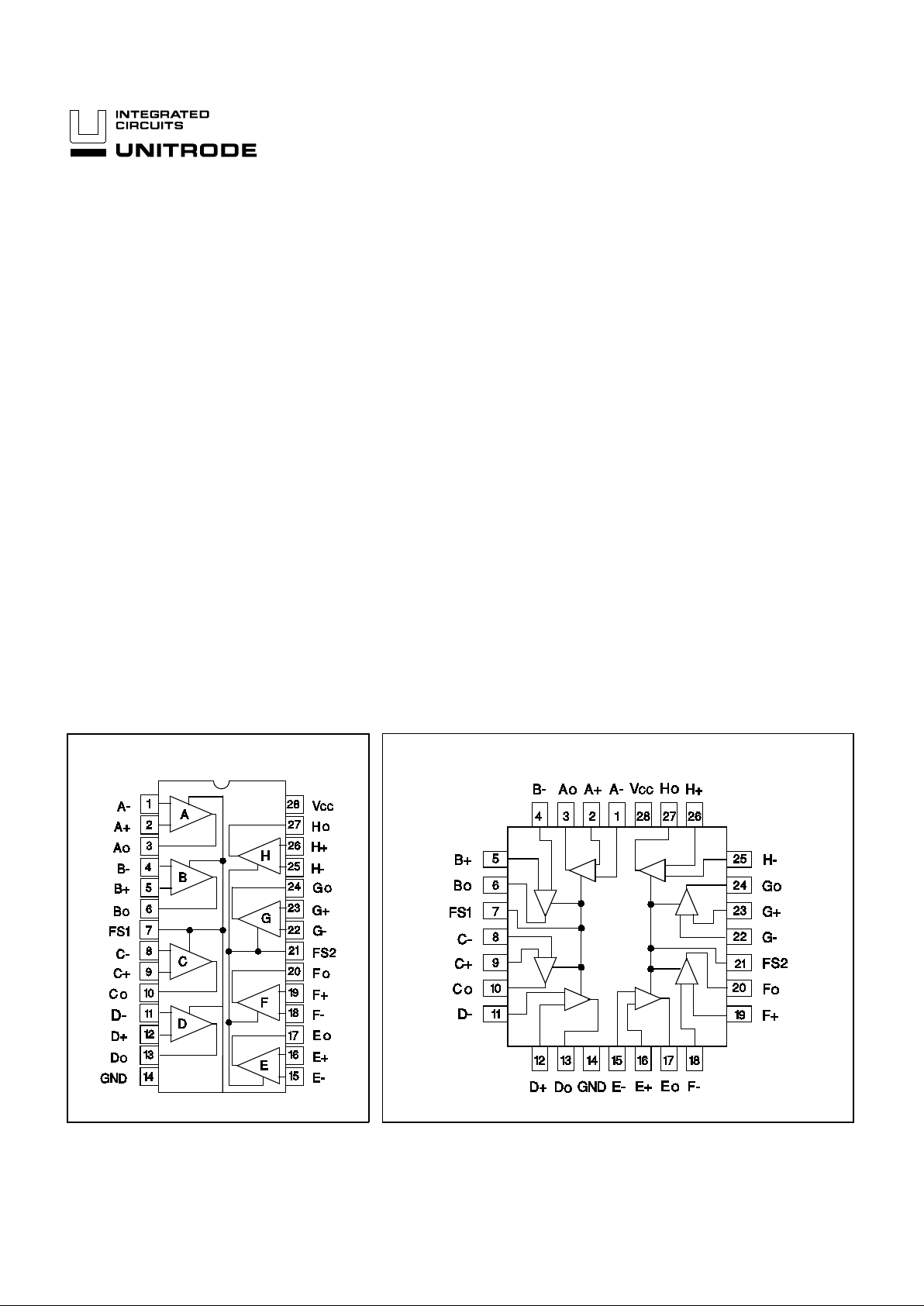
DIL-28 (TOP VIEW)
CONNECTION DIAGRAMS
DESCRIPTION
The UC5180C is an octal l ine receiver designed t o meet a wide range
of digital communications requiremen ts as outlined in EIA standards
EIA232E, EIA423A, EIA422A, and CCITT V.10, V.11, V.28, X.26, and
X.27. The UC5180C includes an input noise filter and is intended for
applications e mployi ng data rates up to 200 KBPS. A failsafe function
allows these de vices to "fail " to a known state under a wide variety of
fault conditions at the inputs.
FEATURES
• Meets EIA 232E/423A/422A and CCITT
V.10,V.11, V.28, X.26, X.27
• Single +5V Supply--TTL Compatible
Outputs
• Differential Inputs Withstand ± 25V
• Low Open Circuit Voltage for Improved
Failsafe Characteristi c
• Reduced Supply Current--35 mA Max
• Input Noise Filter
• Internal Hysteresis
PLCC-28 (TOP VIEW)
1/94

DC ELECTRICAL CHARACTERISTI CS:
PARAMETERS SYMBOL TEST CONDITIONS UC5180C UNITS
MIN MAX
DC Input Resistance R
IN 3V ≤ | VIN | ≤ 25V 3 7 kΩ
Failsafe Output Voltage V
OFS Input s Open or Shorted
Together, or One Input
Open and One Grounde d
0 ≤ IOUT ≤ 8mA, VFAILSAFE = 0V 0.45 V
0 ≥ I
OUT ≥ - 400 µA,
V
FAILSAFE = VCC
2.7
Differential In put High
Threshold
V
TH VOUT = 2.7V, IOUT = 440 µA
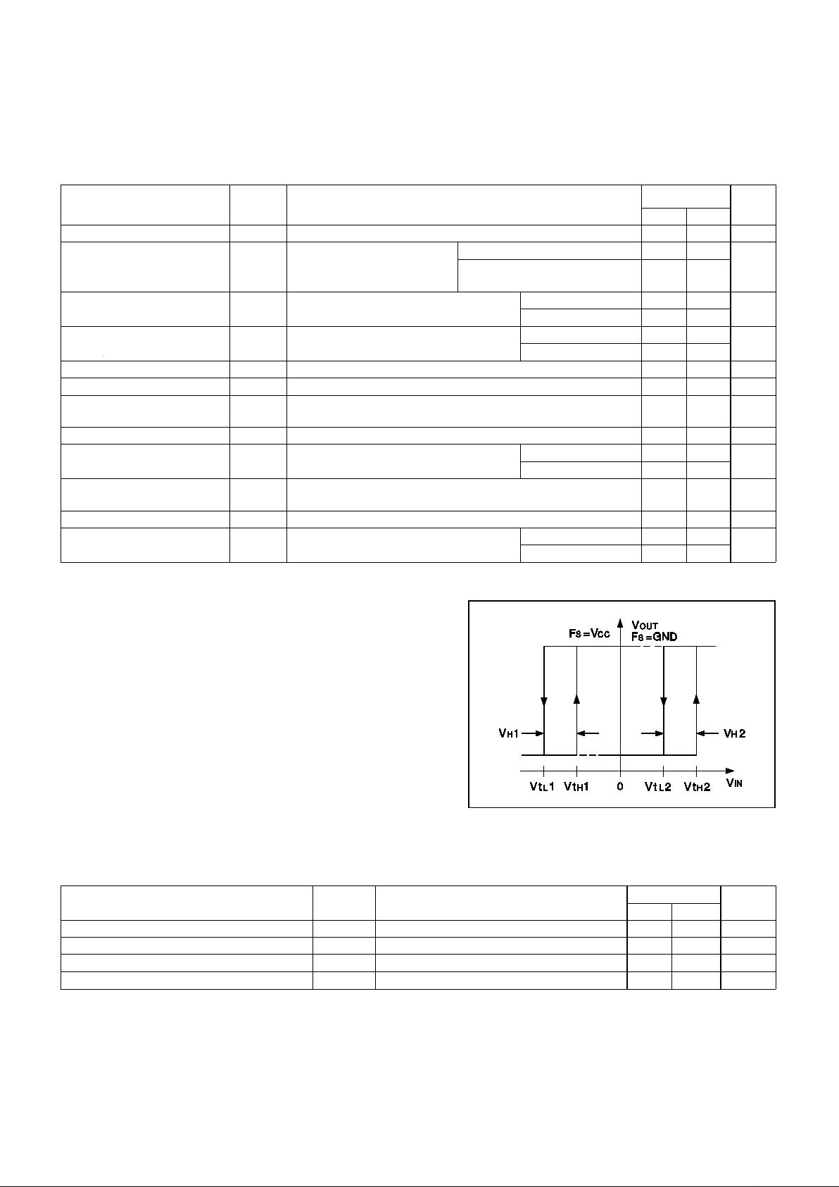
(See Figure 1)
RS = 0 (Note 2) 50 20 0 mV
R
S = 500 (Note 2) 400
Differential In put Low
Threshold
V
TL VOUT = 0.4 5V, IOUT = 440 mA
(See Figure 1)
RS = 0 (Note 2) -200 -5 0 mV
R
S = 500 (Note 2) -400
Hysteresis V
H FS = 0V or VCC (See Figure 1) 50 140 mV
Open Circuit Input Voltage V
ICC 75 mV
Input Capacita nce C
I 20 pF
High Level Output Voltage V
CH VID = 1V, IOUT = - 440 µ A2.7V
Low Level Output Volta ge V
OL VID = -1V
(Note 3)
IOUT = 4 mA 0.4 V
I
OUT = 8 mA 0.45
Short Circuit Output
Current
I
OS Note 4 20 100 mA
Supply Current I
CC 4.75V ≤ VCC ≤ 5.25V 35 mA
Input Curren t I
IN Other Inputs Grounded VIN = +10V 3.25 mA
V
IN
= -10V -3.25
UC5180C
Figure 1. VtL, VtH, VH Def inition
Unless otherwise stated these specifica tion s apply for TA = 0°C to +70°C, V CC
= 5V ± 5%, Input Common Mod e Range ± 7V, TA =TJ
AC ELECTRICAL CHARACTERIS TI CS:
PARAMETERS SYMBOL TEST CONDITION S UC5180C UNITS
MIN MAX
Propagation Delay - Low to High t
PLH CL = 50pF, VIN =
±
500mV 550 ns
Propagation Dela y - High to Low t
PHL CL = 50pF, VIN =
±
500mV 550 ns
Acceptance Input Frequency f
A Unused I npu t Ground ed, VIN = ± 200mV 0.1 MHz
Rejectable Input Frequency f
R Unu sed Inpu t Ground ed, VIN = ± 500m V 5.5 MHz
V
CC = 5V ± 5%, TA = 0°C to + 70°C, Figure 2, TA = TJ.
Note 2: RS is a resistor in series with each input.
Note 3: Measured after 100ms warm up (at 0°C)
Note 4: Only 1 output may be shorted at one time
and then only for a maximum of 1 sec.
2
 Loading...