Phase Locked Frequency Controller
UC1634
UC2634
UC3634
FEATURES
• Precision Phase Locked Frequency Control
System
• Communication Logic for 2-Phase Motors
• Disable Input for Motor Inhibit
• Crystal Oscillator
• Programmable Reference Frequency Dividers
• Phase Detector with Absolute Frequency
Steering
• Digital Lock Indicator
• Two High Current Op-Amps
• 5V Reference Output
DESCRIPTION
The UC1634 series of devices is optimized to provide precision
phase locked frequency control for two phase DC brushless motors. These devices include most of the features of the general
purpose UC1633 Phase Locked Control family and also provide
the out-of-phase commutation signals required for driving two
phase brushless motors. Only an external power booster stage
is required for a complete drive and control system.
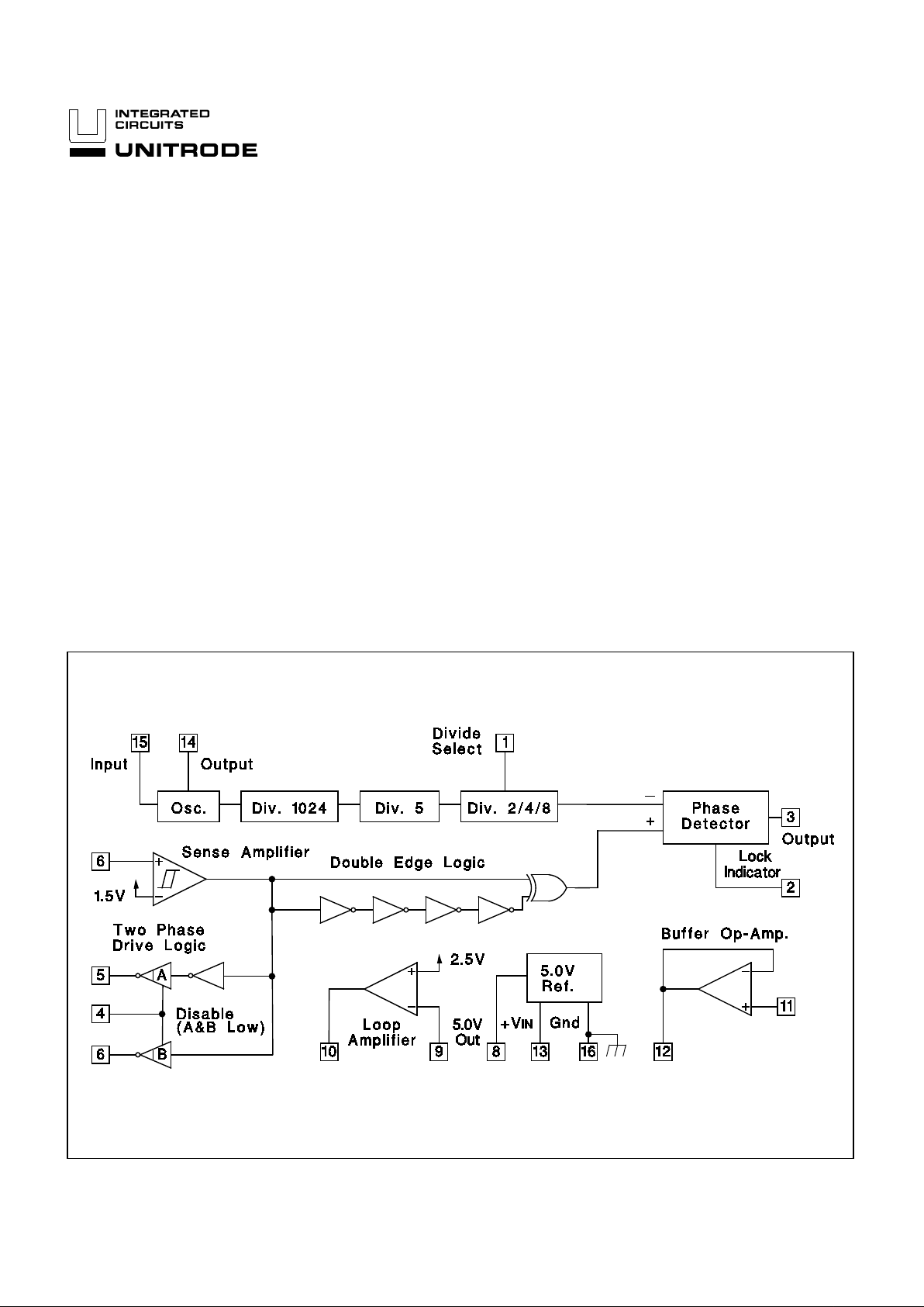
The two commutation outputs are open collector devices that can
sink in excess of 16mA. A disable input allows the user to simultaneously force both of these outputs to an active low state.
Double edge logic, followin g the sense amplifier, doubles the reference frequency at the phase detector by respondi ng to both
edges of the input signal at Pin 7.
BLOCK DIAGRAM
6/93

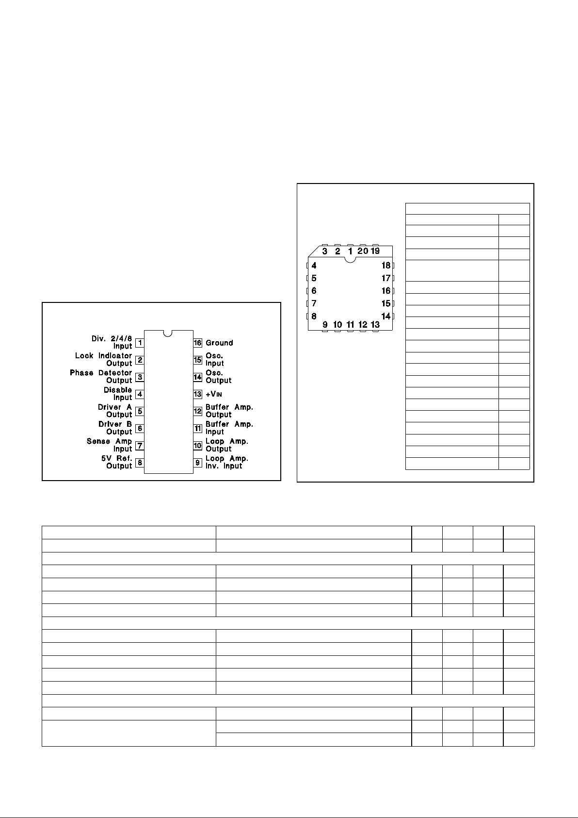
CONNECTION DIAGRAMS
UC1634
UC2634
UC3634
PACKAGE PIN FUNCTION
FUNCTION PIN
N/C 1
DIV 2/4/8 2
Lock Indicator Ou tput 3
Phase Detector
Output
4
Disable Input 5
N/C 6
Driver A Output 7
Driver B Output 8
Sense Amp Output 9
5V Ref Output 10
Loop Amp Inv Input 11
Loop Amp Output 12
Buffer Amp Input 13
Buffer Amp Out put 14
+V
IN 15
N/C 16
OSC Output 17
OSC Input 18
Ground 19
DIV 4/5 Input 20
DIL-16, SOIC- 16 (T O P VIEW)
J or N Package, DW Package
Input Supply Volt age ( +VI N). . . . . . . . . . . . . . . . . . . . . . . . +20V
Reference Output Current . . . . . . . . . . . . . . . . . . . . . . . -30mA
Op-Amp Output Currents . . . . . . . . . . . . . . . . . . . . . . . . ±±30mA
Op-Amp Input Volt ages . . . . . . . . . . . . . . . . . . . . . -.3V to +20V
Phase Detec to r Output Cur ren t . . . . . . . . . . . . . . . . . . . ±±10mA
Lock Indicato r Output Cur ren t . . . . . . . . . . . . . . . . . . . . +15mA
Lock Indicato r Output Volt age . . . . . . . . . . . . . . . . . . . . . . +20V
Divide Select Input Voltage . . . . . . . . . . . . . . . . . . -.3V to +10V
Disable Input Voltage. . . . . . . . . . . . . . . . . . . . . . . -.3V to +10V
Oscillator Input Voltage . . . . . . . . . . . . . . . . . . . . . . -.3V to +5V
Sense Amplifier Input Volta ge . . . . . . . . . . . . . . . . -.3V to +20V
Driver Output Curr ent s. . . . . . . . . . . . . . . . . . . . . . . . . . +30mA
Driver Output Voltag es. . . . . . . . . . . . . . . . . . . . . . . . . . . . +20V
Power Dissipation at T
A = 25°C(Note 2) . . . . . . . . . . . 1000mW
Power Dissipation at T
C = 25°C (Note 2). . . . . . . . . . . 2000mW
Operating Junct ion Te mp era tu re . . . . . . . . . . . -55°C to +150°C
Storage Temperature. . . . . . . . . . . . . . . . . . . . -65°C to +150°C
Lead Tempera tu re (Solderin g, 10 Seconds) . . . . . . . . . . 300°C
PLCC-20 (TOP VIEW)
Q Package
Note 1: V olta ges ar e refe ren ced t o ground , (P in 16, DIL Pack age). Curre nts are posit ive into , negat ive out of , the specifi ed
terminals.
Note 2: Consult Packag in g Sect ion of Dat aboo k for ther ma l
limitations and con sider atio ns of pack age.
ABSOLUTE MAXI MUM RATING S (Note 1, 2)
PARAMETERS TEST CONDITIONS MIN TYP MAX UNITS
Supply Current +VIN = 15V 20 29 mA
Reference
Output Volt age ( VREF
)
4.75 5.0 5.25 V
Load Regulation IOUT = 0mA to 7mA 5.0 20 mV
Line Regulation +VIN = 8V to 15V 2.0 20 mV
Short Circuit Current VOUT = 0V 12 30 mA
Oscillator
DC Voltage Gain Oscillator In to Oscillator Out 12 16 20 dB
Input DC Level (VIB) Oscillator In Pin Open, TJ = 25°C 1.15 1.3 1.45 V
Input Impedance (Note 3) VIN = VIB
±
0.5V, T
J = 25°C 1.3 1.6 1. 9 kΩ
Output DC Level Oscillator In Pin Open, TJ = 25°C 1.2 1.4 1.6 V
Maximum Operating Frequency 10 MHz
Dividers
Maximum Input Frequency Input = 1VPP at Oscillator In 10 MHz
Div. 4/5 Input Current Input = 5V (Div. by 4) 150 500 µA
(Q Package Only, Note 4) Input = 0V (Div. by 5) -5.0 0.0 5.0 µA
Unless other wise stat ed, these specif icat ions ap ply fo r TA = 0°C to +70°C for the
UC3634, -25°C to + 85°C for the UC2634 and -55°C t o +125°C for the UC1634 ,
+VIN
=
12V. TA=TJ.
ELECTRICAL CHARACTERISTICS:
2
 Loading...