

4/97
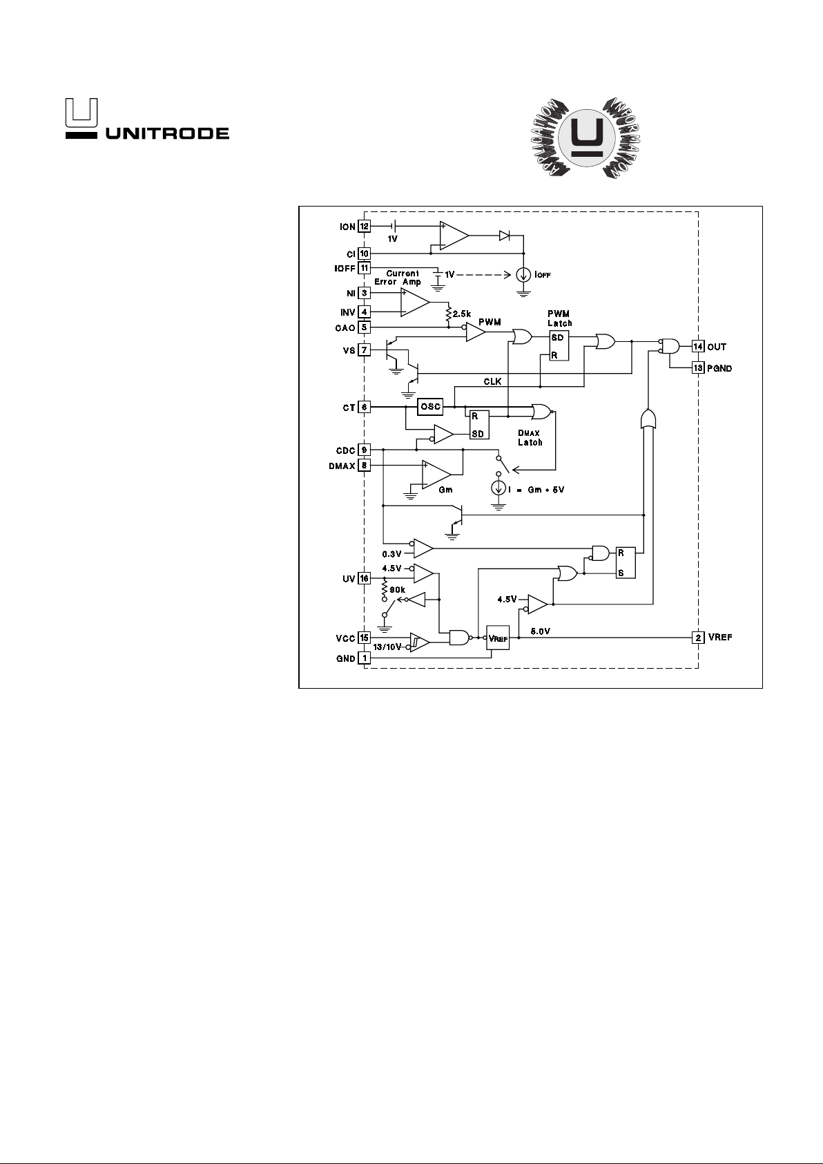
BLOCK DIAGRAM
• Primary Side Voltage Feedforward Control of Isolated Power
Supplies
• Accurate DC Control of
Secondary Side Short Circuit
Current using Primary Side
Average Current Mode Control
• Accurate Programmable
Maximum Duty Cycle Clamp
• Maximum Volt-Second Product
Clamp to Prevent Core Saturation
• Practical Operation Up to 1MHz
• High Current (2A Pk) Totem Pole
Output Driver
• Wide Bandwidth (8MHz) Current
Error Amplifier
• Undervoltage Lockout Monitors
VCC, VIN and VREF
• Output Active Low During UVLO
• Low Startup Current (500µA)
The UC3548 family of PWM control ICs uses voltage fee dforward control to regulate the output voltage of isolated
power supplies. The UC3548 resides on the primary side
and has the necessary features to accurately control secondary side short circuit current with average current
mode control techniques. The UC3548 can be used to
control a wide variety of converter topologies.
In addition to the basic functions required for pulse width
modulation, the UC3548 implements a patented technique
of sensing secondary current from the primary side in an
isolated buck derived converter. A current waveform synthesizer monitors switch current and si m ul at es th e indu cto r
current downslope so that the complete current waveform
can be constructed on the primary side without actual secondary side measurement. This information on the primary
side is used by an average current mode control circuit to
accurately limit maximum output current.
The UC3548 circuitry includes a precision reference, a
wide bandwidth error amplifier for average current control,
an oscillator to generate the system clock, latching PWM
comparator and logic circuits, and a high current output
driver. The current error amplifier easily interfaces with an
optoisolator from a secondary side voltage sensing circuit.
A full featured undervoltage lockout (UVLO) circuit is contained in the UC3548. UVLO monitors the supply voltage
to the controller (VCC), the reference voltage (VREF), and
the input line voltage (VIN). All three must be good before
soft start commences. If either VCC or VIN is low, the supply current required by the chip is only 500µA and the
output is ac tively h eld low.
Two on board protection features set controlled limits to
prevent transformer core saturation. Input voltage is monitored and pulse width is constrained to limit the maximum
volt-second product applied to the transformer. A unique
patented technique limits maximum duty cycle within 3%
of a user programmed value.
These two features allow for more optimal use of transformers and switches, resulting in reduced system size
and cost.
Both patents embodied in the UC3548 belong to Lambda
Electronics Incorporated and are licensed for use in applications emplo yin g th ese devices.
UC1548
UC2548
UC3548
Primary Side PWM Controller
FEATURES
DESCRIPTION
UDG-95037
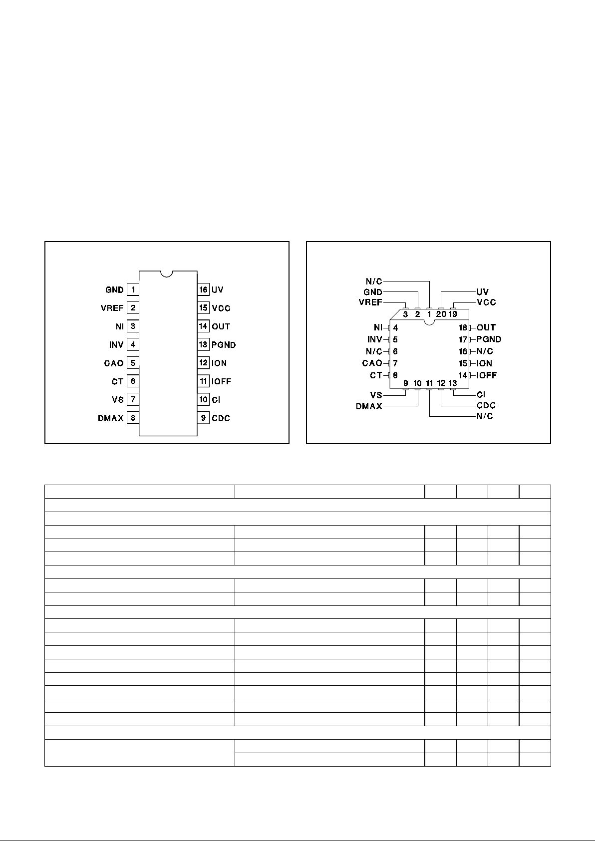
Pin numbers refer to 16-pin DIL and SOIC packages only .
ELECTRICAL CHARACTERISTICS
Unless otherwise stated, all specifications are over the junction temperature range of
−55°C to +125°C for the UC1548, −40°C to +85°C for the UC2548, and 0°C to +70°C for the UC3548. Test conditions are: VCC =
12V, CT = 400pF, CI = 100pF, IOFF = 100µA, CDC = 100nF, Cvs = 100pF, and Ivs = 400µA, TA = TJ.
UC1548
UC2548
UC3548
Supply Voltage (Pin 15) . . . . . . . . . . . . . . . . . . . . . . . . . . . . 22V
Output Current, Source or Sink (Pin 14)
DC . . . . . . . . . . . . . . . . . . . . . . . . . . . . . . . . . . . . . . . . . 0.5A
Pulse (0.5µs) . . . . . . . . . . . . . . . . . . . . . . . . . . . . . . . . . 2.2A
Power Ground to Ground (Pin 1 to Pin 13) . . . . . . . . . . . ±0.2V
Analog Input Voltages
(Pins 3, 4, 7, 8, 12, 16) . . . . . . . . . . . . . . . . . . . . . -0.3 to 7V
Analog Input Currents, Sourc e or Sink
(Pins 3, 4, 7, 8, 11, 12, 16) . . . . . . . . . . . . . . . . . . . . . . 1mA
Analog Output Currents, Sourc e or Sink (Pin s 5 & 10) . . . 5mA
Power Dissipation at TA = 60°C . . . . . . . . . . . . . . . . . . . . . . . . 1W
Storage Temperatur e Ran ge. . . . . . . . . . . . . . . −65°C to +150°C
Lead Temperature (Soldering 10 seconds) . . . . . . . . . . +300°C
CONNECTION DIAGRAMS
PARAMETER TEST CONDITIONS MIN TYP MAX UNITS
Real Time Current Waveform Synthesizer
Ion Amplifier
Offset Voltage 0.95 1 1.05 V
Slew Rate (Note 1) 20 25 V/µs
lib -2 -20 µA
IOFF Current Mirror
Input Voltage 0.95 1 1.05 V
Current Gain 0.911.1A/A
Current Error Amplifier
A
VOL
60 100 dB
Vio 12V ≤ VCC ≤ 20V, 0V ≤ VCM ≤ 5V 10 mV
lib -0.5 -3 µA
Voh I
O
= −200µA 3.1 3.3 3.5 V
Vol I
O
= 200µA0.30.6V
Source Current V
O
= 1V 1.4 1.6 2.0 mA
GBW Product f = 200kHz 5 8 MHz
Slew Rate (Note 1) 810 V/µs
Oscillator
Frequency TA = 25°C 240 250 260 kHz
235 265 kH z
Notes: All voltages are with respect to ground (DIL and SOIC
pin 1). Currents are positive into the specified terminal.
Pin numbers refer to the 16 pin DIL and SO IC packages.
Consult Packaging Section of Databook for thermal
limitations and considerations of packages.
ABSOLUTE MAXIMUM RATINGS
PLCC-20 & LCC-20 (Top View)
Q & L Packages
DIL-16, SOIC-16 (Top View)
J, N, or DW Packages
2
UC1548
UC2548
UC3548
PARAMETER TEST CONDITIONS MIN TYP MAX UNITS
Duty Cycle Clamp
Max Duty Cycle V(D
MAX
) = 0.75 • V
REF
73.5 76.5 79.5 %
VCC Comparator
Turn-on Threshold 13 14 V
Turn-off Threshold 910 V
Hysteresis 2.533.5V
UV Comparator
Turn-on Threshold 4.14.354.6 V
R
HYSTERESIS
Vuv = 4.2V 77 90 103 kΩ
Reference
VREF T
A
= 25°C 4.95 5 5.05 V
0 < I
O
< 10mA, 12 < VCC < 20 4.93 5.07 V
Line Regulation 12V < VCC < 20V 4 15 mV
Load Regulation 0 < I
O
< 10mA 3 15 mV
Short Circuit Current V
REF
= 0V 30 50 70 mA
Output Stage
Rise & Fall Time (Note 1) Cl = 1nF 20 45 ns
Output Low Saturation I
O
= 20mA 0.25 0.4 V
I
O
= 200mA 1.2 2.2 V
Output High Saturation I
O
= -200mA 2.0 3.0 V
UVLO Output Low Saturation IO = 20mA 0.8 1.2 V
I
CC
I
START
VCC = 12V 0.2 0.4 mA
I
CC
(pre-start) VCC = 15V, V(UV) = 0 0.5 1 mA
ICC (run) 22 26 mA
Note 1: Guaranteed by design. Not 100% tested in production.
ELECTRICAL CHARACTERISTICS (cont.):
Unless otherwise stated, all specifications are over the junction
temperature range of −55°C to +125°C for the UC1548, −40°C to +85°C for the UC2548, and 0°C to +70°C for the UC3548. Test
conditions are: VCC = 12 V, C T = 40 0p F, CI = 100 pF , IO F F = 10 0µ A, CDC = 100nF, Cvs = 100pF, and Ivs = 400µA, TA = TJ.
CAO:
Output of the current error amplifier. Also the
resistor load for the collector of an optocoupler.
CDC:
Connect a charge balance integration capacitor
from CDC to GND to achieve an accurate duty cycle
clamp. This capacitor also sets the soft start time.
CI:
Output of th e inductor c urrent waveform synthesizer.
Requires a capacitor to ground.
CT:
A capacitor from CT to GND sets the oscillator
frequency.
DMAX:
Programs maximum duty cycle with a resistive
divider from VREF to DMAX to GND.
GND:
Signal ground.
INV:
Inverting input of the current error amplifier.
IOFF:
Programs the discharge slope of the capacitor on
CI to emulate the down slope of the inductor current
waveform.
ION:
Input pin to inductor current waveform synthesizer.
Apply a voltage proportional to switch current to this pin.
NI:
Noninverting input of the current error amplifier.
OUT
: Output driver for the gate of a power FET.
PGND:
Power ground pin for the output driver. This
ground circuit should be connected to GND at a single
point.
UV:
Line voltage sense pin to insure the chip only
operates with sufficient line voltage. Program with a
resistive divide r from the conver ter input voltage to UV
to GND.
VCC:
Chip supply voltage. Bypass with a 1µF ceramic
capacitor to PGND.
VREF:
Precision voltage reference. Bypass with a 1µF
ceramic capacitor to GND.
VS:
Volt sec ond clamp pr ogramming pin and feedforward
ramp waveform for the puls e wi dth m odulator. Connect a
resistor to the input line voltage and a capacitor to GND.
PIN DESCRIPTIONS
3
 Loading...