

1/97
• Automatic Feed Forward Compensation
• Programmable Pulse-by-Pulse Current
Limiting
• Automatic Symmetry Correction in Push-pull
Configuration
• Enhanced Load Response Characteristics
• Parallel Operation Capability for Modular
Power Systems
• Differential Current Sense Amplifier with
Wide Common Mode Range
• Double Pulse Suppression
• 500mA (Peak) Totem-pole Outputs
•±1% Bandgap Reference
• Under-voltage Lockout
• Soft Start Capability
• Shutdown Terminal
• 500kHZ Operation
Current Mode PWM Controller
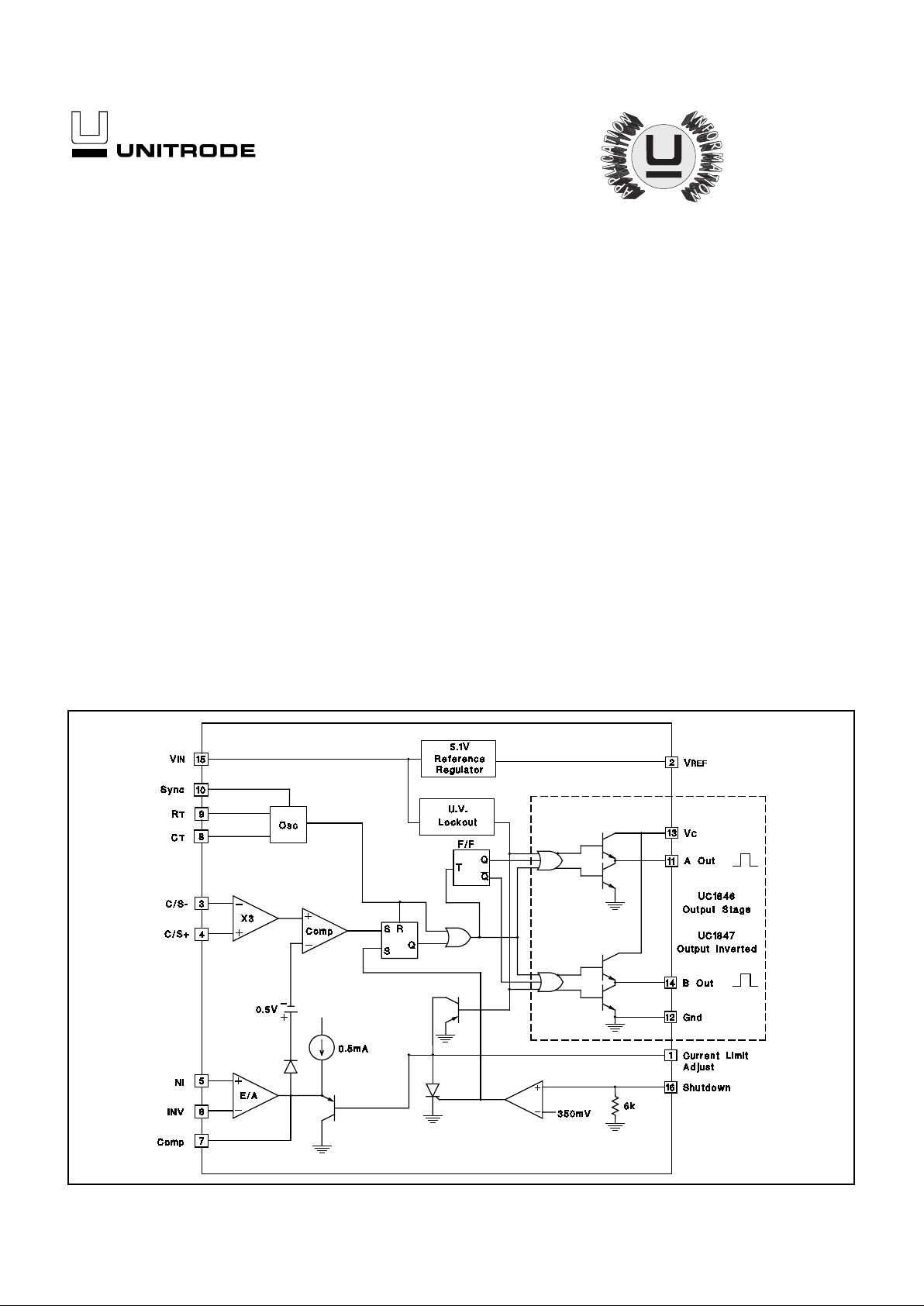
The UC1846/7 family of control ICs provides all of the necessary
features to implement fixed frequency, current mode control
schemes while maintaining a minimum external parts count. The superior performance of this technique can be measured in improved
line regula tion, enhanced load response characteristics, and a simpler, easier-to-design control loop. Topological advantages include
inherent pulse-by-pulse current limiting capability, automatic symmetry corre ction for push -pull convert ers, and the ability to parallel
“power modules" while maintaining equal current sharing.
Protection circuitry includes built-in under-voltage lockout and programmable current limit in addition to soft start capability. A shutdown funct ion is al so avail able whi ch can initiate either a complete
shutdown with automatic restart or latch the supply off.
Other features include fully latched operation, double pulse suppression, deadline adjust capability, and a ±1% trimmed bandgap
reference.
The UC1846 features low outputs in the OFF state, while the
UC1847 features high outputs in the OFF state.
UC1846/7
UC2846/7
UC3846/7
BLOCK DIAGRAM
FEATURES DESCRIPTION
UC1846/7
UC2846/7
UC3846/7
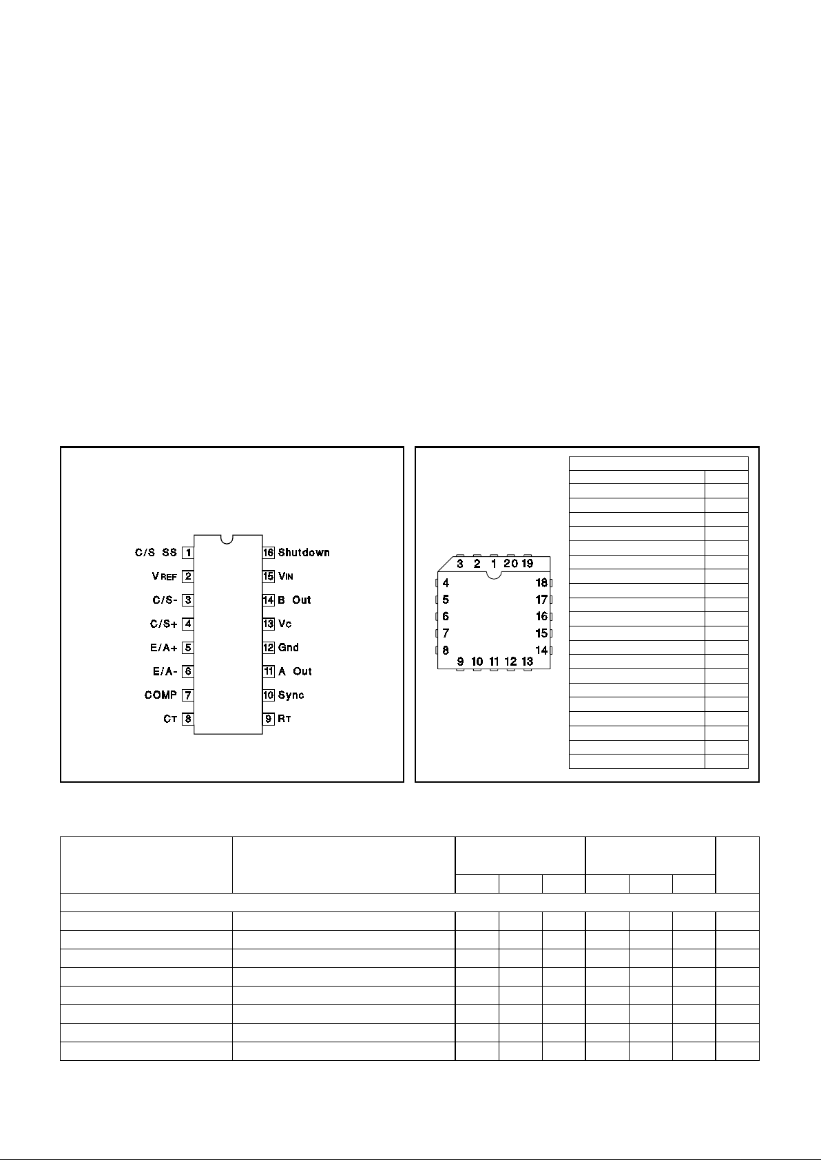
PACKAGE PIN FUNCTION
FUNCTION PIN
N/C
1
C/L SS
2
V
REF
3
C/S-
4
C/S+
5
N/C
6
E/A+
7
E/A-
8
Comp
9
C
T
10
N/C
11
R
T
12
Sync
13
A Out
14
Gnd
15
N/C
16
V
C
17
B Out
18
V
IN
19
Shutdown
20
DIL-16, SOIC-16
(TOP VIEW)
J or N Package, DW Package
CONNECTION DIAGRAMS
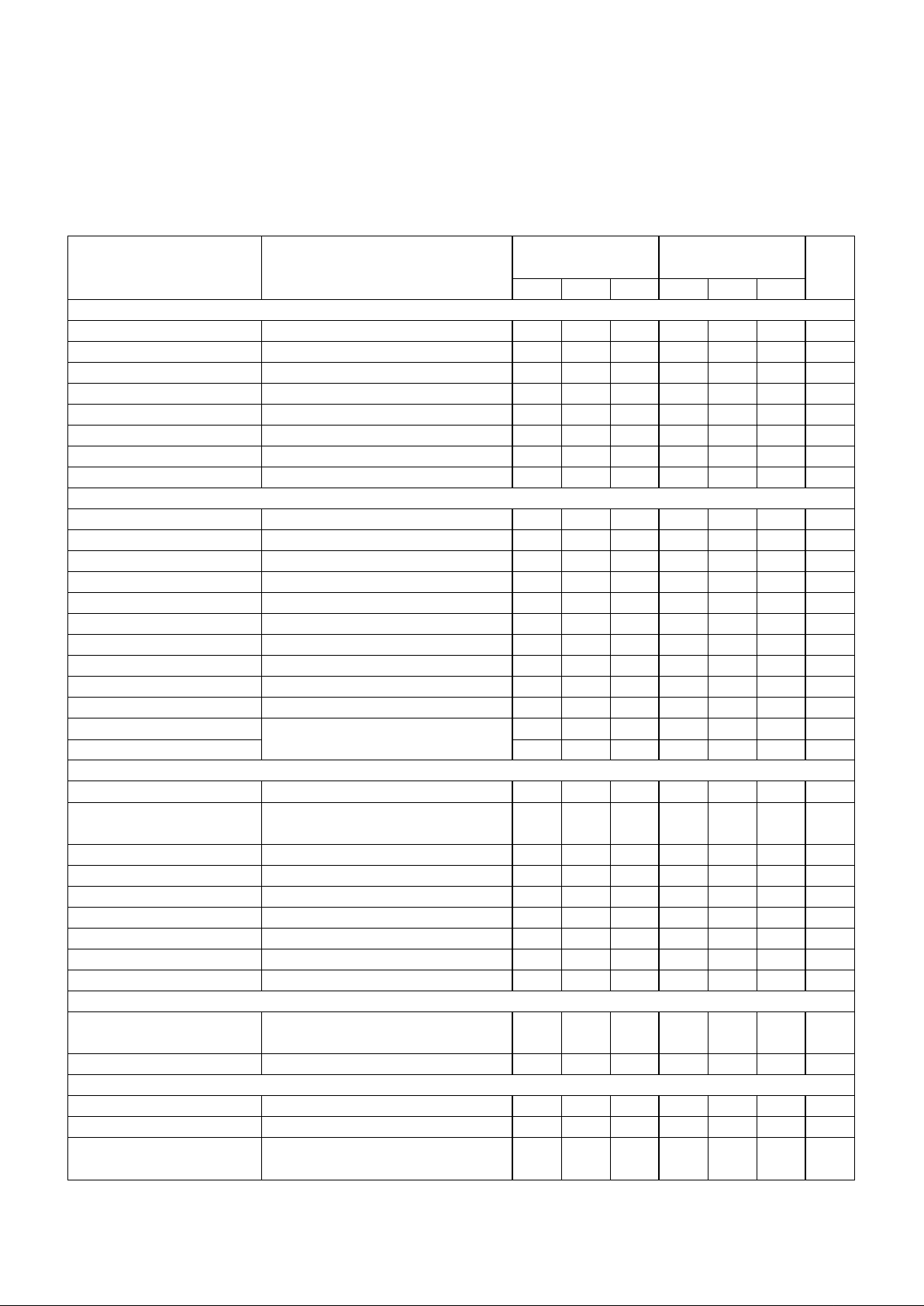
ELECTRICAL CHARACTERISTICS
(Unless otherwise stated, these specifications apply for TA=-55°C to +125°C for
UC1846/7; -40°C to +85°C for th e UC 28 46/7; and 0°C to + 70 °C f or the UC3846/7;
VIN=15V, RT=10k, CT=4.7nF, TA=TJ.)
UC1846/UC1847
UC3846/UC3847
PARAMETER TEST CONDITIONS UC2846/UC2847
MIN. TYP. MAX. MIN. TYP. MAX. UNITS
Reference Section
Output Voltage TJ=25°C, IO=1mA 5.05 5.10 5.15 5.00 5.10 5.20 V
Line Regulation V
IN
=8V to 40V 5 20 5 20 mV
Load Regulation I
L
=1mA to 10mA 3 15 3 15 mV
Temperature Stability Over Operating Range, (Note 2) 0.4 0.4 mV/°C
Total Output Var iation Line, Load, and Te mperature (Not e 2) 5.00 5.20 4.95 5.25 V
Output Noise Voltage 10Hz≤ f ≤10kHz, T
J
=25°C (Note 2) 100 100
µ
V
Long Term Stability T
J
=125°C, 1000 Hrs. (Note 2) 5 5 mV
Short Circuit Output Current V
REF
=0V -10 -45 -10 -45 mA
Supply Voltage (Pin 15) . . . . . . . . . . . . . . . . . . . . . . . . . . . . . . . . . . . . . . . . . +40V
Collector Supply Voltage (Pin 13). . . . . . . . . . . . . . . . . . . . . . . . . . . . . . . . . . +40V
Output Current, Source or Sink (Pins 11, 14). . . . . . . . . . . . . . . . . . . . . . . . 500mA
Analog Inputs (Pins 3, 4, 5, 6, 16) . . . . . . . . . . . . . . . . . . . . . . . . . . . -0.3V to +V
IN
Reference Output Current (Pin 2). . . . . . . . . . . . . . . . . . . . . . . . . . . . . . . . . -30mA
Sync Output Current (Pin 10) . . . . . . . . . . . . . . . . . . . . . . . . . . . . . . . . . . . . . -5mA
Error Amplifier Output Current (Pin 7) . . . . . . . . . . . . . . . . . . . . . . . . . . . . . . -5mA
Soft Start Sink Current (Pin 1) . . . . . . . . . . . . . . . . . . . . . . . . . . . . . . . . . . . . 50mA
Oscillator Charging Current (Pin 9) . . . . . . . . . . . . . . . . . . . . . . . . . . . . . . . . . 5mA
Power Dissipation at TA=25°C . . . . . . . . . . . . . . . . . . . . . . . . . . . . . . . . . 1000mW
Power Dissipation at TC=25°C . . . . . . . . . . . . . . . . . . . . . . . . . . . . . . . . . 20 00mW
Storage Temperature Range . . . . . . . . . . . . . . . . . . . . . . . . . . . . -65°C to +150°C
Lead Temperature (soldering, 10 seconds. . . . . . . . . . . . . . . . . . . . . . . . . +300°C
ABSOLUTE MAXIMUM RATINGS (Note 1)
Note 1. All voltages are with respect to Ground, Pi n 1 3. Currents are positive into,
negative out of the speficied terminal. Consult Packaging Section of Databook for
thermal limitations and considerations of packages. Pin nu mbers refer to DIL and
SOIC packages only.
PLCC-20, LCC-20
(TOP VIEW)
Q, L Packages
2
UC1846/UC1847
UC3846/UC3847
PARAMETER TEST CONDITIONS UC2846/UC2847
MIN. TYP. MAX. MIN. TYP. MAX. UNITS
Oscillator Section
Initial Accuracy TJ=25°C 394347394347kHz
Voltage Stability V
IN
=8V to 40V -1 2 -1 2 %
Temperature Stability Over Operating Range (Note 2) -1 -1 %
Sync Output High Level 3.9 4.35 3.9 4.35 V
Sync Output Low Level 2.3 2.5 2.3 2.5 V
Sync Input High Leve l Pin 8=0V 3.9 3.9 V
Sync Input Low Level Pin 8=0V 2.5 2.5 V
Sync Input Current Sync Voltage=3.9V, Pin 8=0V 1.3 1.5 1.3 1.5 mA
Error Amp Section
Input Offset Volta ge 0.5 5 0.5 10 mV
Input Bias Current -0.6 -1 -0.6 -2
µ
A
Input Offset Current 40 250 40 250 nA
Common Mode Range V
IN
=8V to 40V 0 VIN-2V 0 VIN-2V V
Open Loop Voltage Gai n
∆
V
O
=1.2 to 3V, VCM=2V 80 105 80 105 dB
Unity Gain Bandwidth T
J
=25°C (Note 2) 0.7 1.0 0.7 1.0 MHz
CMRR V
CM
=0V to 38V, VIN=40V 75 100 75 100 dB
PSRR V
IN
=8V to 40V 80 105 80 105 dB
Output Sink Current V
ID
=-15mV to -5V, V
PIN 7
=1.2V 2 6 2 6 mA
Output Source Current V
ID
=15mV to 5V, V
PIN 7
=2.5V -0.4 -0.5 -0.4 -0.5 mA
High Level Output Voltage R
L
=(Pin 7) 15kΩ 4.3 4.6 4.3 4.6 V
Low Level Output Voltage 0.7 1 0.7 1 V
Current Sense Amplifier Section
Amplifier Gain V
PIN 3
=0V, Pin 1 Open (Notes 3 & 4) 2.5 2.75 3.0 2.5 2.75 3.0 V
Maximum Differ en ti al Input Pin 1 Open (Note 3)
Signal (V
PIN 4-VPIN 3
)R
L
(Pin 7)=15kW 1.1 1.2 1.1 1.2 V
Input Offset Voltage V
PIN 1
=0.5V, Pin 7 Open (Note 3) 5 25 5 25 mV
CMRR V
CM
=1V to 12V 6083 6083 dB
PSRR V
IN
=8V to 40V 6084 6084 dB
Input Bias Current V
PIN 1
=0.5V, Pin 7 Open (Note 3) -2.5 -10 -2.5 -10
µ
A
Input Offset Current V
PIN 1
=0.5V, Pin 7 Open (Note 3) 0.08 1 0.08 1
µ
A
Input Common Mode Range 0 V
IN
-3 0 VIN-3 V
Delay to Outputs T
J
=25°C, (Note 2) 200 500 200 500 ns
Current Limit Adjust Section
Current Limit Offset V
PIN 3
=0V, V
PIN 4
=0V, Pin 7 Open
(Note 3) 0.45 0.5 0.55 0.45 0.5 0.55 V
Input Bias Current V
PIN 5=VREF
, V
PIN 6
=0V -10 -30 -10 -30
µ
A
Shutdown Terminal Section
Threshold Voltage 250 350 400 250 350 400 mV
Input Voltage Range 0 V
IN
0V
IN
V
Minimum Latching Current (Note 6)
(I
PIN 1
) 3.0 1.5 3.0 1.5 mA
ELECTRICAL
CHARACTERISTICS (cont.)
(Unless otherwise stated, these specifications apply for TA=-55°C to +125°C for UC1846/7; -40 °C
to +85°C for the UC2846/7; and 0°C to +7 0°C for the UC384 6/7; VIN=15V, RT=10k, CT=4.7nF,
TA=TJ.)
UC1846/7
UC2846/7
UC3846/7
3

Note 2. These parameters, although guaranteed over the recommended operating conditions, are not 100% tested in production.
Note 3. Parameter measured at trip point of latch with V
PIN 5
= V
REF
, V
PIN 6
= 0V.
Note 4. Amplifier gain defined as: G
=
∆
V
PIN
7
∆
V
PIN
4
; ∆
V
PIN
4
= 0 to
1.0V.
Note 5. Applies to UC1 84 6/ U C28 46/UC3846 only due t o po la rit y of outputs.
Note 6. Current into Pin 1 guaranteed to latch circuit in shutdown state.
Note 7. Current into Pin 1 guaranteed not to latch circuit in shutdown state.
UC1846/7
UC2846/7
UC3846/7
UC1846/UC1847
UC3846/UC3847
PARAMETER TEST CONDITIONS UC2846/UC2847
MIN. TYP. MAX. MIN. TYP. MAX. UNITS
Shutdown Terminal Sectio n (co nt. )
Maximum Non-Latching (Note 7)
Current (I
PIN 1
) 1.5 0.8 1.5 0.8 mA
Delay to Outputs T
J
=25°C (Note 2) 300 600 300 600 ns
Output Section
Collector-Emitter Voltage 40 40 V
Collector Leakage Curre nt V
C
=40V (Note 5) 200 200
µ
A
Output Low Level I
SINK
=20mA 0.1 0.4 0.1 0.4 V
I
SINK
=100mA 0.4 2.1 0.4 2.1 V
Output High Level I
SOURCE
=20mA 1313.5 1313.5 V
I
SOURCE
=100mA 12 13.5 12 13.5 V
Rise Time C
L
=1nF, TJ=25°C (Note 2) 50 300 50 300 ns
Fall Time C
L
=1nF, TJ=25°C (Note 2) 50 300 50 300 ns
Under-Voltage Lockout Section
Start-Up Threshold 7.7 8.0 7.7 8.0 V
Threshold Hysteresis 0.75 0.75 V
Total Standby Current
Supply Current 17 21 17 21 mA
Oscillator Circuit
Output deadtime is determined by the external capacitor, CT, according to the formula:
τ
d
(µs) =
145C
T
(
µf
)
I
D
ID −
3.6
RT (kΩ
)
.
For large values of R
T
:
τ
d
(µs) ≈
145C
T
(
µf
)
.
Oscillator frequency is approximated by the formula:
f
T
(
kHz
) ≈
2.2
R
T
(k
Ω)•
CT
(
µ
f
)
.
ELECTRICAL
CHARACTERISTICS (cont.)
(Unless otherwise stated, these specifications apply for TA=-55°C to +125°C for UC1846/7; -40 °C
to +85°C for the UC2846/7; and 0°C to +7 0°C for the UC384 6/7; VIN=15V, RT=10k, CT=4.7nF,
TA=TJ.)
APPLICATIONS DATA
ID = Oscillator discharge current at 25°C is typically 7.5.
4

Error Amp Output Configuration
Error Amp Open-Logic D.C. Gain vs Load Resistan ce
Error Amp Gain and Phase vs Frequency
UC1846/7
UC2846/7
UC3846/7
APPLICATIONS DATA (cont.)
Parallel Operation
5

Pulse by Pulse Current Limiting
Soft Start and Shutdown /Restart Function s
UC1846/7
UC2846/7
UC3846/7
Peak Current (IS) is determined by the formula: I
S
=
R
2
V
REF
R
1
+
R
2
−
0.5
3R
S
APPLICATIONS DATA (cont.)
6

Current Sense Amp Connecti on
UC1846 Open Loop T es t Circuit
UC1846/7
UC2846/7
UC3846/7
UNITRODE CORPORATI ON
7 CONTINENTAL BLVD. • MERRIMACK, NH 03054
TEL. (603) 424- 24 10 • FAX (603)424-3460
APPLICATIONS DATA (cont.)
A small RC fi lt er ma y be required in some applic at io ns t o red uc e swi t c h tra ns ie nt s.
Differential input allow s remote, noise free sensing.
7

IMPORTANT NOTICE
T exas Instruments and its subsidiaries (TI) reserve the right to make changes to their products or to discontinue
any product or service without notice, and advise customers to obtain the latest version of relevant information
to verify, before placing orders, that information being relied on is current and complete. All products are sold
subject to the terms and conditions of sale supplied at the time of order acknowledgement, including those
pertaining to warranty, patent infringement, and limitation of liability.
TI warrants performance of its semiconductor products to the specifications applicable at the time of sale in
accordance with TI’s standard warranty. Testing and other quality control techniques are utilized to the extent
TI deems necessary to support this warranty. Specific testing of all parameters of each device is not necessarily
performed, except those mandated by government requirements.
CERT AIN APPLICATIONS USING SEMICONDUCT OR PRODUCTS MAY INVOLVE POTENTIAL RISKS OF
DEATH, PERSONAL INJURY, OR SEVERE PROPERTY OR ENVIRONMENTAL DAMAGE (“CRITICAL
APPLICATIONS”). TI SEMICONDUCTOR PRODUCTS ARE NOT DESIGNED, AUTHORIZED, OR
WARRANTED TO BE SUITABLE FOR USE IN LIFE-SUPPORT DEVICES OR SYSTEMS OR OTHER
CRITICAL APPLICATIONS. INCLUSION OF TI PRODUCTS IN SUCH APPLICA TIONS IS UNDERSTOOD T O
BE FULLY AT THE CUSTOMER’S RISK.
In order to minimize risks associated with the customer’s applications, adequate design and operating
safeguards must be provided by the customer to minimize inherent or procedural hazards.
TI assumes no liability for applications assistance or customer product design. TI does not warrant or represent
that any license, either express or implied, is granted under any patent right, copyright, mask work right, or other
intellectual property right of TI covering or relating to any combination, machine, or process in which such
semiconductor products or services might be or are used. TI’s publication of information regarding any third
party’s products or services does not constitute TI’s approval, warranty or endorsement thereof.
Copyright 1999, Texas Instruments Incorporated
 Loading...