

Page 1
查询TRF1223供应商
.ti.com
www
TRF1223
SLWS166A–APRIL2005–REVISEDJULY2005
3.3-GHzTO3.8-GHZ1-WPowerAmplifier
FEATURES
VPOS
VNEG
•1WP-1dBLinear,30-dBGainTransmitter
•OperatesOverthe3300-MHzto3800-MHz
Range
•TwoTTLControlled,1-bit,16-dBGainSteps
for32dBofTotalGainControl
•SuperiorLinearity(+45dBmIP3)Overthe
EntireFrequencyRange
VDD
RFO
Power
Supply
Power
Amp /
Attenuator
Driver
Amplifier
Pre-Amp
ACNT
P
LP
RFI
•Auto-BiasDesignWithPAEnable
•TemperatureCompensatedDirectional
CouplerDetector
•LowPowerBiasMode
DETN
DETP
•InternallyMatched50-ΩInputandOutput
AGAIN1
P
AGAIN0
P
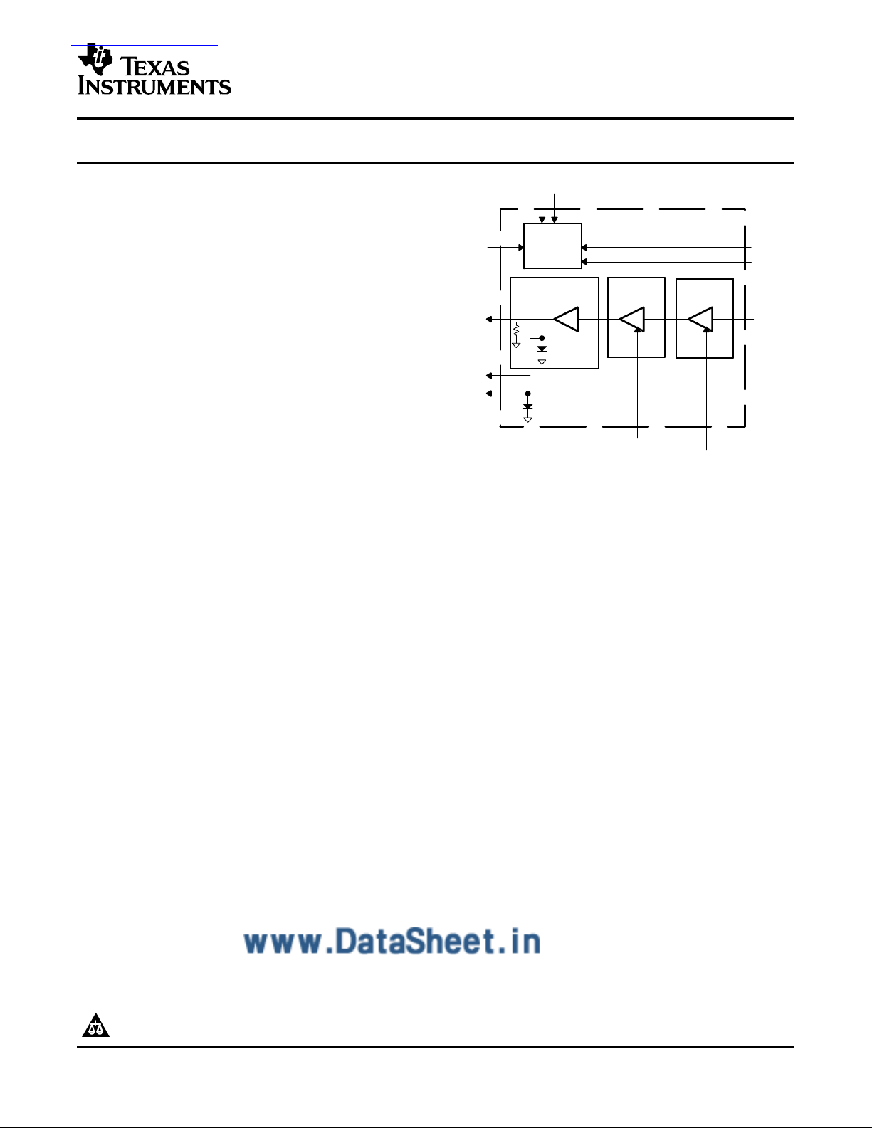
DESCRIPTION
TheTRF1223isahighlyintegratedlineartransmitter/poweramplifier(PA)MMIC.Thechiphastwo16-dBgain
stepsthatprovideatotalof32-dBgaincontrolvia1-bitTTLcontrolsignals.ThechipalsointegratesaTTLmute
functionthatturnsofftheamplifiersforpowercriticalorTDDapplications.Atemperaturecompensateddetector
isincludedforoutputpowermonitororALCapplications.ThechiphasaP
interceptof+45dBm.
TheTRF1223isdesignedtofunctionasapartofTexasInstrumentscomplete3.5-GHzchipset.TheTRF1223is
theoutputpoweramplifieroradriveramplifierforhigherpowerapplications.Thelinearnatureofthetransmitter
makesitidealforcomplexmodulationsschemessuchashighorderQAMorOFDM.
of+30dBmandathirdorder
1dB
KEYSPECIFICATIONS
•OP
•OutputIP3=+45dBm,Typical
•Gain=30dB,Typical
•GainFlatnessoverTransmitBand±2dB
•FrequencyRange=3300MHzto3800MHz
•±0.5-dBDetectedOutputVoltagevsTemperature
=+30dBm
1dB
BLOCKDIAGRAM
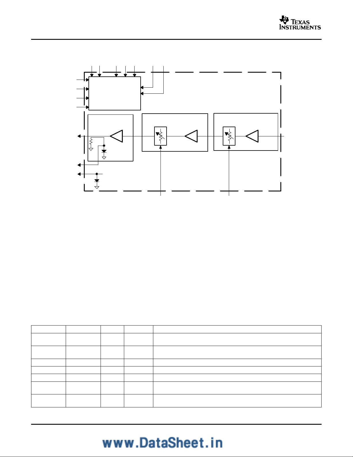
Thedetailedblockdiagramandthepin-outoftheASICareshowninFigure1.
Pleasebeawarethatanimportantnoticeconcerningavailability,standardwarranty,anduseincriticalapplicationsofTexas
Instrumentssemiconductorproductsanddisclaimerstheretoappearsattheendofthisdatasheet.
PRODUCTIONDATAinformationiscurrentasofpublicationdate.
ProductsconformtospecificationsperthetermsoftheTexas
Instrumentsstandardwarranty.Productionprocessingdoesnot
necessarilyincludetestingofallparameters.
Copyright©2005,TexasInstrumentsIncorporated
Page 2
TRF1223
SLWS166A–APRIL2005–REVISEDJULY2005
www
.ti.com
VDD1
VDD2
VDD3A
VDD3B
RFO
DETN
DETP
VPOS
VNEG
Power
Attenuator
Power
Supply
Amp /
ADJ1
V
VADJ2
VADJ3
Switched
PACNT
LP
Attn
PAGAIN1
Figure1.DetailedBlockDiagramofTRF1223
Driver Amp
Switched
PAGAIN0
Attn
Pre-Amp
RFI
ELECTROSTATICDISCHARGENOTE
TheTRF1223containClass1devices.Thefollowingelectrostaticdischarge(ESD)precautionsarerecommended:
•Protectiveoutergarments
•HandlinginESDsafeguardedworkarea
•TransportinginESDshieldedcontainers
•FrequentmonitoringandtestingallESDprotectionequipment
•TreatingtheTRF1223asextremelysensitivetoESD
PINOUTTABLE
Table1.PinOutofTRF1223
PIN#PINNAMEI/OTYPEDESCRIPTION
1VDD1IPowerStage1dcdrainsupplypower.Thedccurrentthroughthispinistypically5%of
IDD.
2VADJ1IAnalogNoconnectionrequiredfornormaloperation.MaybeusedtoadjustFET1bias.
DONOTGROUNDTHISPINORCONNECTTOANYOTHERPIN.
3GND--Ground
4RFIIAnalogRFinputtopoweramplifier,dcblockedinternally
5RFIIAnalogRFinputtopoweramplifier,dcblockedinternally
6VNEGIPowerNegativepowersupply–5V.Usedtosetgatevoltage.Thisvoltagemustbe
sequencedwithVDD.See
7VPOSIPowerPositivepowersupplyforbiascircuits.Biasis+5V.Usedtosetgatebiasand
logicinputlevel.
(1)
(1)
.
(1)Propersequencing:Inordertoavoidpermanentdamagetothepoweramplifier,thesupplyvoltagesmustbesequenced.Theproper
powerupsequenceisV
2
,thenV
NEG
,andthenVDD.TheproperpowerdownsequenceisremoveVDD,thenV
POS
POS
,andthenV
.
NEG
Page 3
www.ti.com
SLWS166A – APRIL 2005 – REVISED JULY 2005
Table 1. Pin Out of TRF1223 (continued)
PIN # PIN NAME I/O TYPE DESCRIPTION
8 PAGAIN0 I Digital First 16-dB attenuator gain control. Logic high is high gain and logic low is low
gain.
9 PAGAIN1 I Digital Second 16-dB gain control. Logic high is high gain and logic low is low gain.
10 VADJ2 I Analog No connection required for normal operation. May be used to adjust FET2 bias.
DO NOT GROUND THIS PIN OR CONNECT TO ANY OTHER PIN.
11-14 GND - - Ground
15 VADJ3 I Analog No connection required for normal operation. May be used to adjust FET3 bias
DO NOT GROUND THIS PIN OR CONNECT TO ANY OTHER PIN.
16 LP I Digital Low power mode: Active high. Low power mode is lower dc and P
17 PACNT I Digital Power amplifier enable, High is PA on, logic low is PA off (low current)
18 VDD3B I Power Stage 3 dc-drain supply power. This pin is internally dc connected to pin 23
(VDD3A). Bias must be provided to both pins for optimal performance. The total
dc-current through these two pins is typically 70% of IDD.
19 GND - - Ground
20 RFO O Analog RF output, internal dc block
21 RFO O Analog RF output, internal dc block
22 VDD3A - - Ground
23 DETP I Power Stage 3 dc-rain supply power. This pin is internally dc connected to pin 18
(VDD3B). Bias must be provided to both pins for optimal performance. The total
dc-current through these two pins is typically 70% of IDD.
24 DETN O Analog Detector output, positive. Voltage will be 0.5 V with/without RF output
25 GND O Analog Detector output, negative. Voltage is 0.5 V with no RF and decreases with
increasing RF output power.
26-31 GND - - Ground
32 VDD2 I Power Stage 2 dc-drain supply power. The dc current through this pin is typically 25%
of IDD.
Back - - Back of package has a metal base which must be grounded for thermal and RF
performance.
TRF1223
mode.
OUT
SPECIFICATIONS
ABSOLUTE MAXIMUM RATINGS
PARAMETER TEST CONDITION MIN MAX UNIT
VDD 0 8 V
VPOS DC supply voltage 0 5.5 V
VNEG -5.5 0 V
I
DD
Pin RF input power 20 dBm
T
j
Pd Power dissipation 6.5 W
Θ
jc
T
stg
T
op
(1) Thermal resistance is junction to case assuming thermal pad with 25 thermal vias under package metal base. See the recommended
layout Figure 7 and application note RA1005 for more detail.
Current consumption 1300 Ma
Junction temperature 175 °C
Digital input pins -0.3 5.5
Thermal resistance junction to 20 °C/W
(1)
case
Storage temperature -40 105 °C
Operating temperature Maximum case temperature derate for -40 85 °C
PCB thermal resistance
Lead temperature 40 sec maximum 220 °C
3
Page 4

www.ti.com
TRF1223
SLWS166A – APRIL 2005 – REVISED JULY 2005
DC CHARACTERISTICS
PARAMETER CONDITIONS MIN TYP MAX UNIT
V
DD
I
DD
I
DD
V
NEG
I
NEG
V
POS
I
POS
V
IH
V
IL
I
IH
I
IL
VDD supply voltage -40°C, PACNTRL = High, 5 7 V
VDD supply current high power 925 mA
VDD supply current low power 550 mA
Negative supply voltage -40°C, PACNTRL = High, -5.25 -5 -4.75 V
Negative supply current 25°C, PACNTRL = High, 15 25 mA
Positive supply digital voltage 85°C, PACNTRL = High, 4.75 5 5.25 V
Positive supply digital current 35 50 mA
Input high voltage 2.5 5 V
Input low voltage 0.8 V
Input high current 300 µA
Input low current -50 µA
V
= 5 V, LP = Low
DD
25°C, PACNTRL = High,
V
= 5 V, LP = Low
DD
85°C, PACNTRL = High,
V
= 5 V, LP = Low
DD
V
= 5 V, LP = High, 25°C
DD
V
= 5 V, LP = High, 25°C
DD
V
= 5 V, LP = High, 25°C
DD
875
950
475
600
POWER AMPLIFIER CHARACTERISTICS
Unless otherwise stated: V
25°C
PARAMETER TEST CONDITIONS MIN TYP MAX UNIT
F Frequency 3300 3800 MHz
G Gain 26 30 32.5 dB
σ
G
G
HG
G
NB
OP-1dB Output power at 1-dB compression High power bias mode 30 31 dBm
OP-1dB Output power at 1-dB compression Low power bias mode 27 dBm
OIP3 Output third order intercept point High power bias mode 43 48 dBm
OIP3 Output third order intercept point Low power bias mode 38 dBm
Vdet Detector voltage output, differential At POUT = 27 ±0.75 dBm, 150 mV
t
STEP
P
ON/OFF
NF
HG
NF
LG
S
12
S
11
S
22
Standard deviation part-to-part gain At a single frequency, full gain 0.3 dB
Gain flatness full band F = 3300 MHz to 3800 MHz 4 6 dB
Gain flatness / 2 MHz 0.2 dB
(DETP-DETN) F = 3300 MHz to 3800 MHz at 25°C
Detector accuracy vs temperature F = 3550 MHz, -30 to 75°C, ±0.5 dB
Gain step size 1st step PAGAIN0 = Low, PAGAIN1 = High 13 16 19 dB
Gain step size 2nd step PAGAIN0 = Low, PAGAIN1 = Low 26 32 38 dB
Gain step response time 1 5 µs
On to Off Power ratio Max gain-to-gain with PACNT = Low 35 dB
Noise figure, max gain PAGAIN0 = High, PAGAIN1 = High 6 7 dB
Noise figure min gain PAGAIN0 = Low, PAGAIN1 = Low 20 dB
Reverse isolation 30 dB
Input return loss Z = 50 Ω -10 -12 dB
Output return loss Z = 50 Ω -8 dB
= 5 VS, IDD= 1050 mA, V
DD
= 5 V, V
POS
= -5 V, PAGAIN0 = 1, PAGAIN1 = 1, PACNT = 1, T =
NEG
4
Page 5

www.ti.com
ATTEN = 10 dB
RL = −8 dB
RBW = 3 kHz
VBW = 3 kHz
SWP = 6.02 sec.
0
0.2
0.4
0.6
0.8
1
1.2
1.4
1.6
1.8
0 5
10 15 20 25 30 35
TA = −40C
TA = 25C
TA = 85C
RC1223B Detector Output
3.5 GHz
Voltage Dector − V
PO − Output Power − dBm
0
0.2
0.4
0.6
0.8
1
1.2
1.4
1.6
1.8
0 5
10
15
20 25 30 35
3.8 GHz
RC1223B Detector Output
TA = 25C
Voltage Dector − V
PO − Output Power − dBm
3.3 GHz
3.5 GHz
TRF1223
SLWS166A – APRIL 2005 – REVISED JULY 2005
TYPICAL PERFORMANCE
All data was taken on parts mounted on PCBs using the pad layout specified in Figure 7 and the filled via
process illustrated in Figure 8 .
Figure 2. Pulse Droop Figure 3. Detector vs Temperature
Figure 4. Detector Output vs Frequency
5
Page 6

www.ti.com
TRF1223
SLWS166A – APRIL 2005 – REVISED JULY 2005
APPLICATION INFORMATION
6
Page 7

www.ti.com
1
2
5
4
3
6
7
8
9 10 131211 14 15 16
17
18
19
20
VDD1
VADJ1
GND
RFI
RFI
PAGAIN1
VADJ2
GND
BASE
VDD
21
22
24
2526272829303132
VNEG
VPOS
PAGAIN0
GND
GND
GND
VADJ3
LP
PACNT
VDD3B
GND
RFO
RFO
GND
VDD3A
DETP
DETN
GND
GND
GND
GND
GND
GND
VDD2
VNEG
PACNT
PAGAIN1
PAGAIN0
RFI
VPOS
23
RFO
RFI
Vdet
LP
10 µF*
1 µF
100 pF
.01 µF
.01 µF
100 pF
1 µF
.01 µF
100 pF
1 µF
.01 µF
100 pF
Place 100 pF Capacitors
Close to Package Pins.
*100 pF Maybe Required for
High Speed Pulse Application
**1 kΩ Resistors on Digital Inputs are required to Prevent Possible Device
Damage Due to ESD and/or Over Voltage
1 kΩ **
1 kΩ **
1 kΩ **
1 kΩ **
100 pF
.01 µF
100 pF
.01 µF
SLWS166A – APRIL 2005 – REVISED JULY 2005
APPLICATION INFORMATION (continued)
A typical application schematic is shown in Figure 5 and a mechanical drawing of the package outline (LPCC
Quad 5 mm x 5 mm, 32-pin) is shown in Figure 6 .
The recommended PCB Layout mask is shown in Figure 7 below, along with recommendations on the board
material Table 2 and construction Figure 8 .
TRF1223
Figure 5. Recommended TRF1223 Application Schematic
Figure 6. Package Drawing
Table 2. PCB Recommendations
Board Material FR4
Board Material Core Thickness 10 mil
Copper Thickness (starting) 1 oz
Recommended Number of Layers 4
Via Plating Thickness 0.5 oz
Prepreg Thickness 8 mil
7
Page 8

www.ti.com
0.25 TYP
0.75 TYP
0.75 TYP
SOLDER MASK: NO SOLDERMASK UNDER CHIP, ON LEAD PADS
OR ON GROUND CONNECTIONS.
25 VIA HOLES, MIN, EACH 0.38 mm.
DIMENSIONS in mm
DIA 0.38
TYP
0.60 TYP
3.50
3.50
3.80
0.50 TYP
0.20 TYP
PIN 1
Additional Copper
Ground and via Holes at
Customer Discreation
TRF1223
SLWS166A – APRIL 2005 – REVISED JULY 2005
Table 2. PCB Recommendations (continued)
Final Plate White immersion tin
Final Board Thickness 33 to 37 mil
Figure 7. Recommended Pad Layout
8
Page 9

www.ti.com
8 Mil
Prepreg
Dia 15 Mil
10 Mil Core FR4
10 Mil Core FR4
1 oz Copper
1 oz Copper
DuPont CB 100 Conductive Via Plug
1/2 oz Copper Plated
1 oz Copper + 1/2 oz Copper Plated
Upper and Lower Surfaces
35 Mil
W1
W2
D1
Feed Direction
D2
P
Figure 8. Via Cross Section
TRF1223
SLWS166A – APRIL 2005 – REVISED JULY 2005
Figure 9. Tape and Reel Specification
9
Page 10

IMPORTANT NOTICE
Texas Instruments Incorporated and its subsidiaries (TI) reserve the right to make corrections, modifications,
enhancements, improvements, and other changes to its products and services at any time and to discontinue
any product or service without notice. Customers should obtain the latest relevant information before placing
orders and should verify that such information is current and complete. All products are sold subject to TI’s terms
and conditions of sale supplied at the time of order acknowledgment.
TI warrants performance of its hardware products to the specifications applicable at the time of sale in
accordance with TI’s standard warranty. Testing and other quality control techniques are used to the extent TI
deems necessary to support this warranty . Except where mandated by government requirements, testing of all
parameters of each product is not necessarily performed.
TI assumes no liability for applications assistance or customer product design. Customers are responsible for
their products and applications using TI components. To minimize the risks associated with customer products
and applications, customers should provide adequate design and operating safeguards.
TI does not warrant or represent that any license, either express or implied, is granted under any TI patent right,
copyright, mask work right, or other TI intellectual property right relating to any combination, machine, or process
in which TI products or services are used. Information published by TI regarding third-party products or services
does not constitute a license from TI to use such products or services or a warranty or endorsement thereof.
Use of such information may require a license from a third party under the patents or other intellectual property
of the third party, or a license from TI under the patents or other intellectual property of TI.
Reproduction of information in TI data books or data sheets is permissible only if reproduction is without
alteration and is accompanied by all associated warranties, conditions, limitations, and notices. Reproduction
of this information with alteration is an unfair and deceptive business practice. TI is not responsible or liable for
such altered documentation.
Resale of TI products or services with statements different from or beyond the parameters stated by TI for that
product or service voids all express and any implied warranties for the associated TI product or service and
is an unfair and deceptive business practice. TI is not responsible or liable for any such statements.
Following are URLs where you can obtain information on other Texas Instruments products and application
solutions:
Products Applications
Amplifiers amplifier.ti.com Audio www.ti.com/audio
Data Converters dataconverter.ti.com Automotive www.ti.com/automotive
DSP dsp.ti.com Broadband www.ti.com/broadband
Interface interface.ti.com Digital Control www.ti.com/digitalcontrol
Logic logic.ti.com Military www.ti.com/military
Power Mgmt power.ti.com Optical Networking www.ti.com/opticalnetwork
Microcontrollers microcontroller.ti.com Security www.ti.com/security
Telephony www.ti.com/telephony
Video & Imaging www.ti.com/video
Wireless www.ti.com/wireless
Mailing Address: Texas Instruments
Post Office Box 655303 Dallas, Texas 75265
Copyright 2005, Texas Instruments Incorporated
 Loading...