TRF1015
RF DOWNCONVERTER
SLWS021D– JUNE 1996 – REVISED JULY 1998
1
POST OFFICE BOX 655303 • DALLAS, TEXAS 75265
D
Low-Noise Amplifier (LNA), Radio
Frequency (RF) Mixer, and
Voltage-Controlled Oscillator (VCO)
D
Improved Compression Mode
D
Conversion From RF to Intermediate
Frequency (IF) on a Single Chip
D
Suitable for Portable 900-MHz Cellular and
Cordless Telephones
D
Low-Current Consumption Mode
D
20-Pin Plastic Shrink Small Outline (SSOP)
Package
D
Application-Selectable Internal or External
Oscillator
description
The Texas Instruments (TI) TRF1015 is a single-chip RF downconverter suitable for 900-MHz receiver
applications. It combines a low-noise amplifier (LNA), a buffered voltage-controlled oscillator (VCO), and an RF
mixer into a 20-pin SSOP package requiring very few external components.
Minimal power consumption can be further reduced by placing the required modules into operate mode and the
remaining modules into standby mode.
Three modes of operation are provided for both the LNA and the mixer: standby, low current, and improved
compression. The improved compression mode is suitable for applications that require full duplex capability.
The improved compression mode is suitable for maintaining receiver sensitivity in the presence of large
interfering signals and provides a low bit-error rate (BER) in digital modulation systems. The three modes of
operation are selectable in accordance with the presence of a high or low signal on PD1 and PD2, as shown
in Table 1.
Table 1. Mode Control
MODE PD1 PD2
Standby L L
Low current H H
Improved compression L H
The LNA has a gain of 13 dB and a noise figure of 2.2 dB. LNA input and output characteristic impedances are
50 Ω. The single balanced RF mixer has a gain of 9 dB with a single-sideband (SSB) noise figure of 10 dB. The
VCO has a typical tuning range of 25 MHz using an external varactor and resonator. The VCO gain and tuning
range can be adjusted to meet the phase-locked loop (PLL) design requirement, with an external shunt and
feedback capacitors in series with the resonator. A buf fered output of the VCO provides phase locking capability
and can be configured for single-ended or differential operation.
The TRF1015 is offered in the 20-pin SSOP (DB) package and is characterized for operation from – 40°C
to 85°C free-air temperature.
These devices have limited built-in ESD protection. The leads should be shorted together or the device placed in conductive foam
during storage or handling to prevent electrostatic damage to the MOS gates.
Please be aware that an important notice concerning availability, standard warranty, and use in critical applications of
Texas Instruments semiconductor products and disclaimers thereto appears at the end of this data sheet.
PRODUCTION DATA information is current as of publication date.
Products conform to specifications per the terms of Texas Instruments
standard warranty. Production processing does not necessarily include
testing of all parameters.
Copyright 1998, Texas Instruments Incorporated
1
2
3
4
5
6
7
8
9
10
20
19
18
17
16
15
14
13
12
11
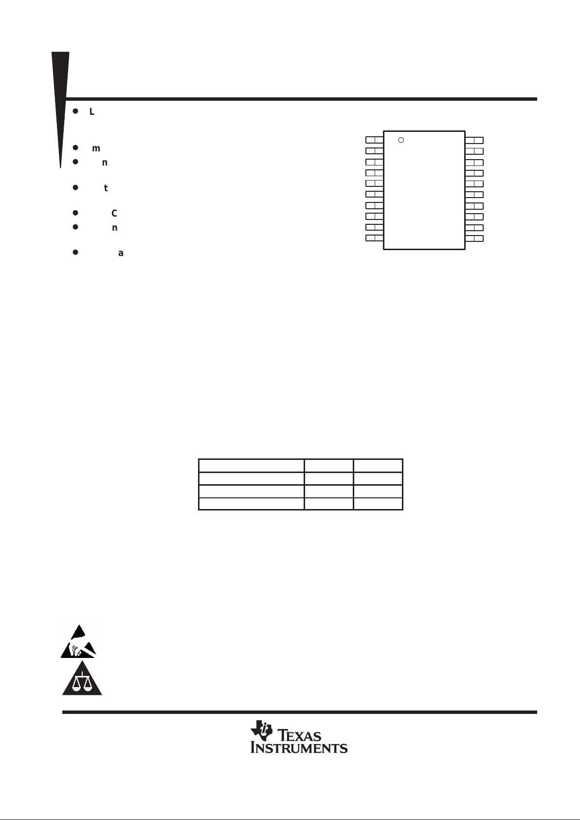
PD1
PD2
AUX_LO–
AUX_LO+
OSC2
VCO_GND
OSC1
VCO_V
CC
VCO_BYP
LNA_GND
MIX_OUT–
MIX_OUT+
MIX_IN
MIX_GND
LNA_GND
LNA_IN
LNA_V
CC
LNA_OUT
LNA_GND
LNA_GND
DB PACKAGE
(TOP VIEW)
TI is a trademark of Texas Instruments Incorporated.
TRF1015
RF DOWNCONVERTER
SLWS021D– JUNE 1996 – REVISED JULY 1998
2
POST OFFICE BOX 655303 • DALLAS, TEXAS 75265
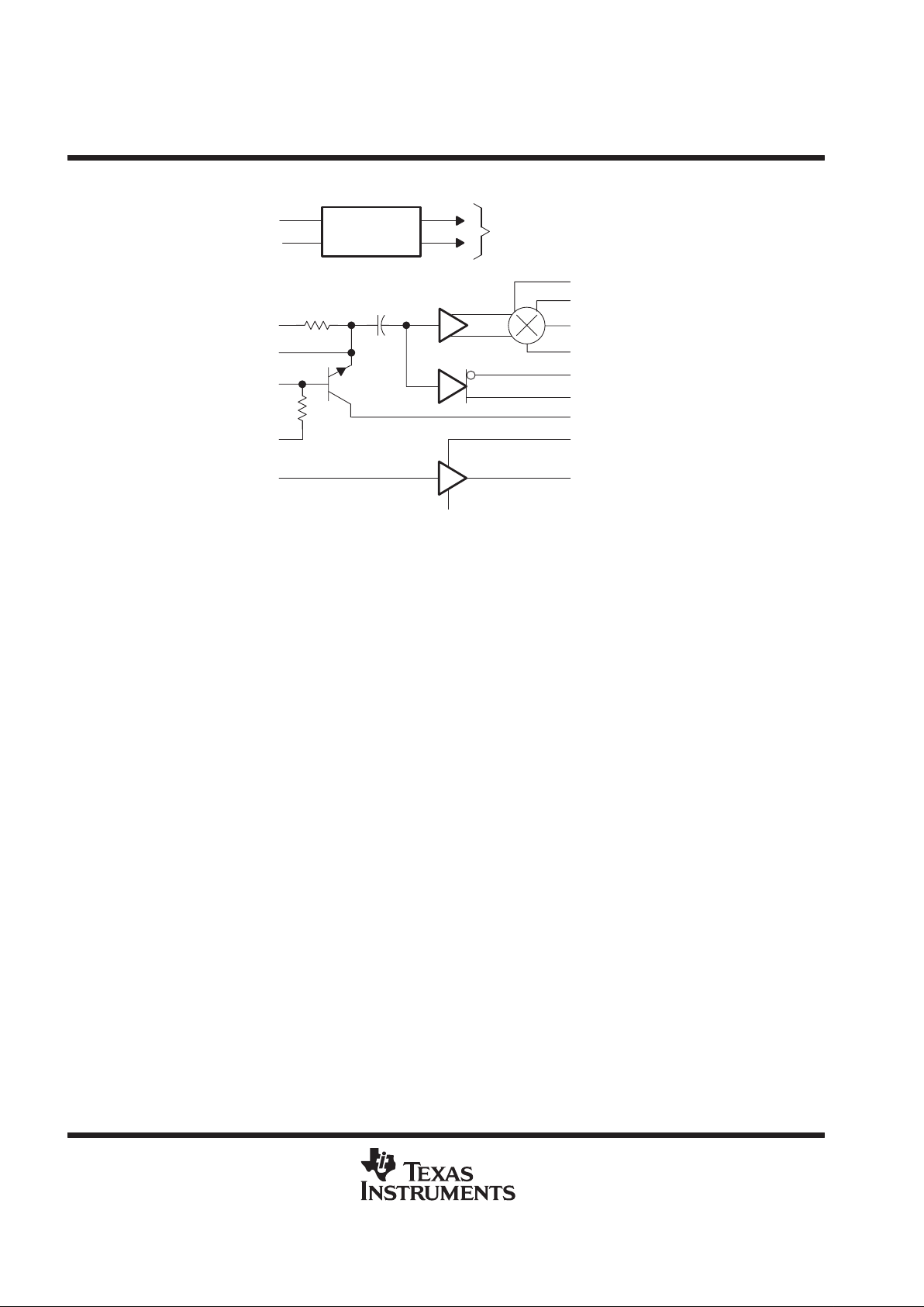
functional block diagram
20
19
18
17
3
4
8
10, 11, 12, 16
13
6
5
7
9
15
MIX_OUT–
MIX_OUT+
MIX_IN
MIX_GND
AUX_LO–
AUX_LO+
VCO_V
CC
LNA_GND
LNA_OUT
VCO_GND
OSC2
VCO_BYP
OSC1
LNA_IN
LNA_V
CC
14
Power Down
Logic
Power-Down Signal
To On-Board Circuits
Buffer
Amp
Buffer
Amp
1
2
PD1
PD2
TRF1015
RF DOWNCONVERTER
SLWS021D– JUNE 1996 – REVISED JULY 1998
3
POST OFFICE BOX 655303 • DALLAS, TEXAS 75265
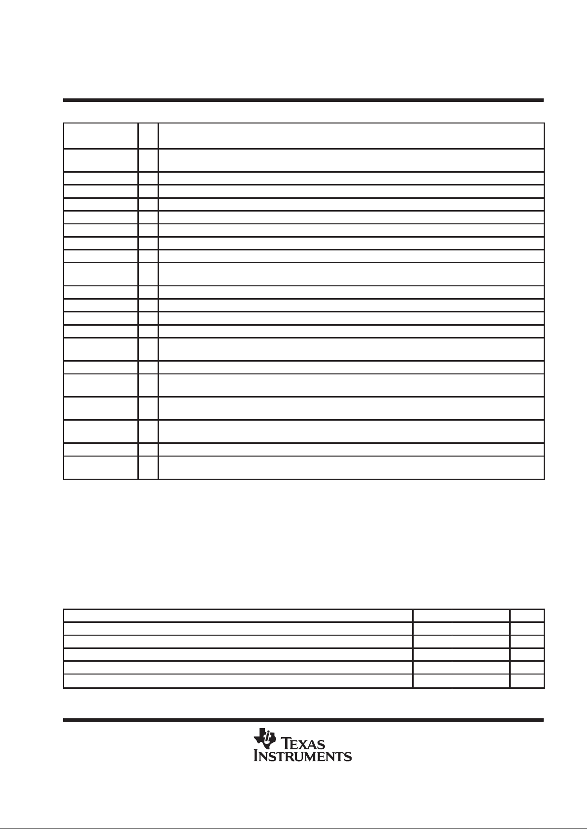
Terminal Functions
TERMINAL
NAME NO.
I/O
DESCRIPTION
AUX_LO– 3 O PLL auxiliary local oscillator (LO) output (inverting). AUX_LO – is the inverted output from the auxiliary local
oscillator.
AUX_LO+ 4 O PLL auxiliary LO output (noninverting). AUX_LO+ is the noninverted output from the auxiliary local oscillator.
LNA_GND 10 LNA ground
LNA_GND 11 LNA ground
LNA_GND 12 LNA ground
LNA_GND 16 LNA ground
LNA_IN 15 I LNA RF input. LNA_IN is the RF input signal to the LNA.
LNA_OUT 13 O LNA RF output. LNA_OUT is the RF output from the LNA.
LNA_V
CC
14 LNA voltage supply. The power supply voltage required to operate the LNA is connected to LNA_VCC. See
Application Information section.
MIX_GND 17 Mixer ground
MIX_IN 18 I Mixer RF input. MIX_IN is the RF input to the mixer.
MIX_OUT– 20 O Mixer IF output (inverting). MIX_OUT– is the inverted intermediate frequency (IF) output from the mixer.
MIX_OUT+ 19 O Mixer IF output (noninverting). MIX_OUT+ is the noninverted intermediate frequency (IF) output from the mixer.
OSC1 7 VCO tank port. A coaxial resonator and other tuning components are connected to OSC1 to form the local oscillator
(see Application Information section).
OSC2 5 External oscillator input. An external oscillator can be connected to OSC2. See Application Information section.
PD1 1 I Power down 1 LSB. PD1, along with PD2, determines which sections of the TRF1015 are placed in standby or
operate mode.
PD2 2 I Power down 2 MSB. PD2, along with PD1, determines which sections of the TRF1015 are placed in standby or
operate mode.
VCO_BYP 9 VCO bypass port. An external capacitor can be connected to VCO_BYP when the TRF1015 is configured for local
oscillator operation.
VCO_GND 6 VCO ground
VCO_V
CC
8 VCO voltage supply. The power supply voltage required to operate the VCO is connected to VCO_VCC (see
Application Information section).
absolute maximum ratings over operating free-air temperature range (unless otherwise noted)
Supply voltage range, VCC –0.3 V to 6 V. . . . . . . . . . . . . . . . . . . . . . . . . . . . . . . . . . . . . . . . . . . . . . . . . . . . . . . . . .
Input voltage range, V
I
–0.3 V to VCC + 0.3 V. . . . . . . . . . . . . . . . . . . . . . . . . . . . . . . . . . . . . . . . . . . . . . . . . . . . . .
Power dissipation at or below T
A
= 25°C 200 mW. . . . . . . . . . . . . . . . . . . . . . . . . . . . . . . . . . . . . . . . . . . . . . . . . . .
Operating virtual-junction temperature, T
J
150°C. . . . . . . . . . . . . . . . . . . . . . . . . . . . . . . . . . . . . . . . . . . . . . . . . . .
Operating free-air temperature range, T
A
–40°C to 85°C. . . . . . . . . . . . . . . . . . . . . . . . . . . . . . . . . . . . . . . . . . . .
Storage temperature range, T
stg
–65°C to 125°C. . . . . . . . . . . . . . . . . . . . . . . . . . . . . . . . . . . . . . . . . . . . . . . . . . .
recommended operating conditions
MIN NOM MAX UNIT
Supply voltage, V
CC
3.5 3.75 5.5 V
High-level input voltage, V
IH
VCC–0.5 V
CC
V
Low-level input voltage, V
IL
–0.3 0.5 V
Operating free-air temperature, T
A
–40 85 °C
Operating virtual-junction temperature, T
J
–30 105 °C
TRF1015
RF DOWNCONVERTER
SLWS021D– JUNE 1996 – REVISED JULY 1998
4
POST OFFICE BOX 655303 • DALLAS, TEXAS 75265
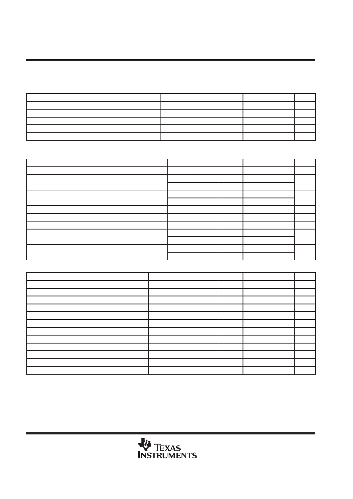
electrical characteristics at 881 MHz, TA = 25°C, LO = 926 MHz, VCC = 3.75 V; measured in
recommended application circuit board (see Application Information)
cascade (LNA/SAW†/mixer) (IF = 45 MHz)
PARAMETER TEST CONDITIONS MIN TYP MAX UNIT
Power conversion gain PD1 = L, PD2 = H 18 19 21 dB
SSB noise figure PD1 = L, PD2 = H 4.2 5 dB
Input 1-dB compression point PD1 = L, PD2 = H –26 dBm
Input 3rd-order intercept point, 2f2 – f
1
PD1 = L, PD2 = H –19 –14 dBm
LO feedthrough to RF –45 dBm
†
Surface acoustic wave (SAW)
LNA
PARAMETER TEST CONDITIONS MIN TYP MAX UNIT
RF frequency range 869 894 MHz
PD1 = H, PD2 = H 12
Power gain
PD1 = L, PD2 = H 13
dB
PD1 = H, PD2 = H 2
Noise figure
PD1 = L, PD2 = H 2.2
dB
Reverse isolation PD1 = L, PD2 = H –25 dB
Input return loss ZI = 50 Ω, PD1 = L, PD2 = H –10 dB
Output return loss ZO = 50 Ω, PD1 = L, PD2 = H –12 dB
p
p
PD1 = H, PD2 = H –19
Input 1-dB compression
PD1 = L, PD2 = H –14
dBm
p
p
p
PD1 = H, PD2 = H –12
Input 3rd-order intercept point, 2f
2
–
f
1
PD1 = L, PD2 = H –4
dBm
RF mixer
PARAMETER TEST CONDITIONS MIN TYP MAX UNIT
RF frequency range 869 894 MHz
LO frequency range 914 939 MHz
IF frequency 45 MHz
Power conversion gain PD1 = L, PD2 = H 9 dB
SSB noise figure PD1 = L, PD2 = H 10 dB
RF input impedance 50 Ω
LO input impedance External VCO 50 Ω
RF input return loss OSC1 = ZI = 50 Ω –10 dB
LO input return loss OSC1 = ZI = 50 Ω –6 dB
IF output return loss OSC1 = ZO = 50 Ω PD1 = L, PD2 = H –15 dB
Input 1-dB compression point PD1 = L, PD2 = H –10 dBm
Input 3rd-order intercept point, 2f2 – f
1
PD1 = L, PD2 = H 1 dBm
TRF1015
RF DOWNCONVERTER
SLWS021D– JUNE 1996 – REVISED JULY 1998
5
POST OFFICE BOX 655303 • DALLAS, TEXAS 75265
electrical characteristics at 881 MHz, TA = 25°C, LO = 926 MHz, VCC = 3.75 V; measured in
recommended application circuit board (see Application Information) (continued)
VCO
PARAMETER TEST CONDITIONS MIN TYP MAX UNIT
Auxiliary LO output power RL = 50 Ω –11 dBm
Phase noise Offset = 60 kHz –114 dBc/Hz
Harmonics –20 dBc
standby mode requirements over recommended operating free-air temperature range and
V
CC
= 3.75 V; (PD1 = L, PD2 = L)
MIN TYP MAX UNIT
LNA 28 100 µA
RF mixer and buffer amplifier 100 µA
VCO 100 µA
low current mode requirements over recommended operating free-air temperature range and
V
CC
= 3.75 V; (PD1 = H, PD2 = H)
MIN TYP MAX UNIT
LNA 2 3 mA
RF mixer and buffer amplifier 14 17 mA
VCO 4 5 mA
improved compression mode requirements over recommended operating free-air temperature
range and V
CC
= 3.75 V; (PD1 = L, PD2 = H)
MIN TYP MAX UNIT
LNA 5 7 mA
RF mixer and buffer amplifier 15 19 mA
VCO 3.75 4.5 mA
TRF1015
RF DOWNCONVERTER
SLWS021D– JUNE 1996 – REVISED JULY 1998
6
POST OFFICE BOX 655303 • DALLAS, TEXAS 75265
APPLICATION INFORMATION
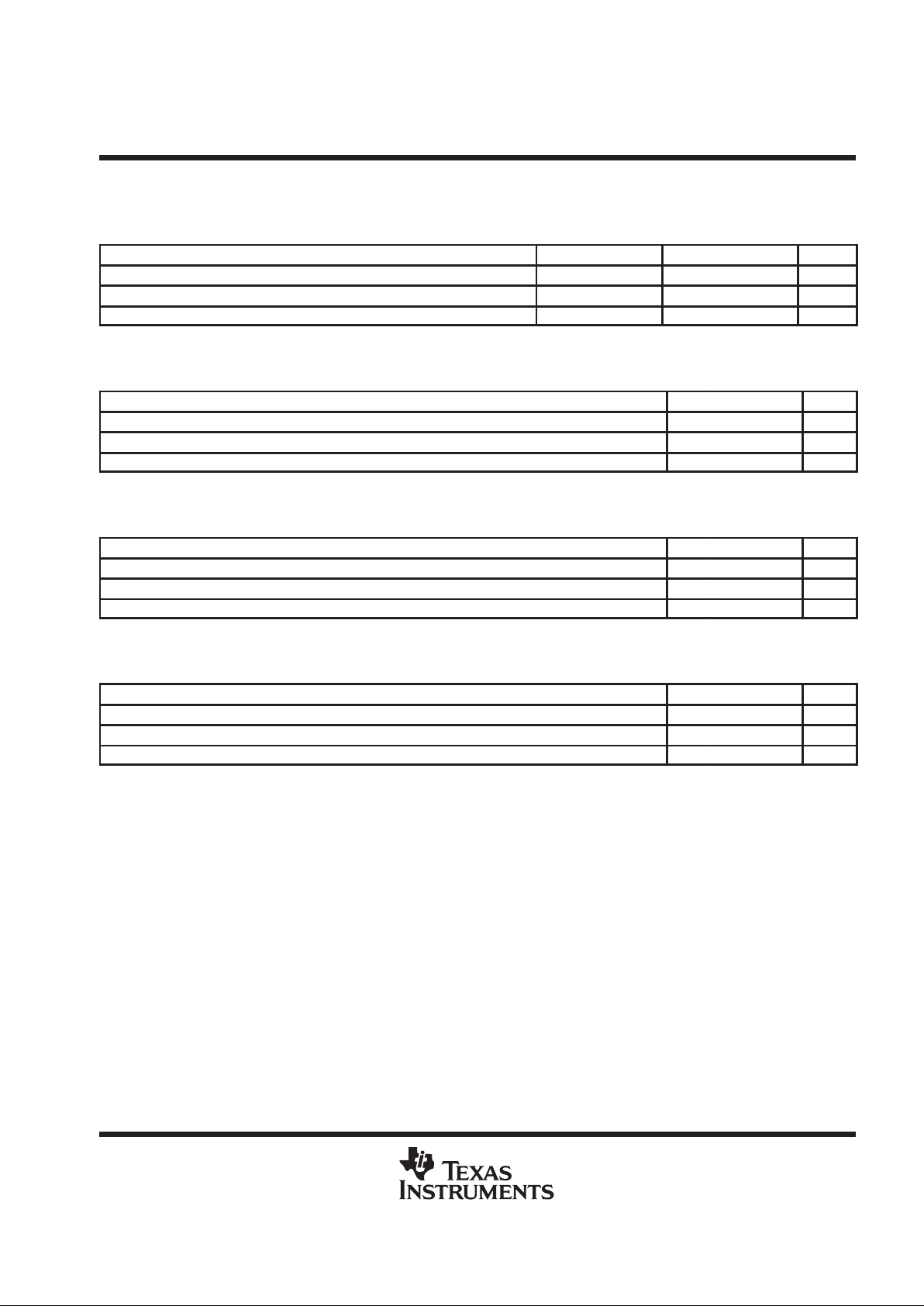
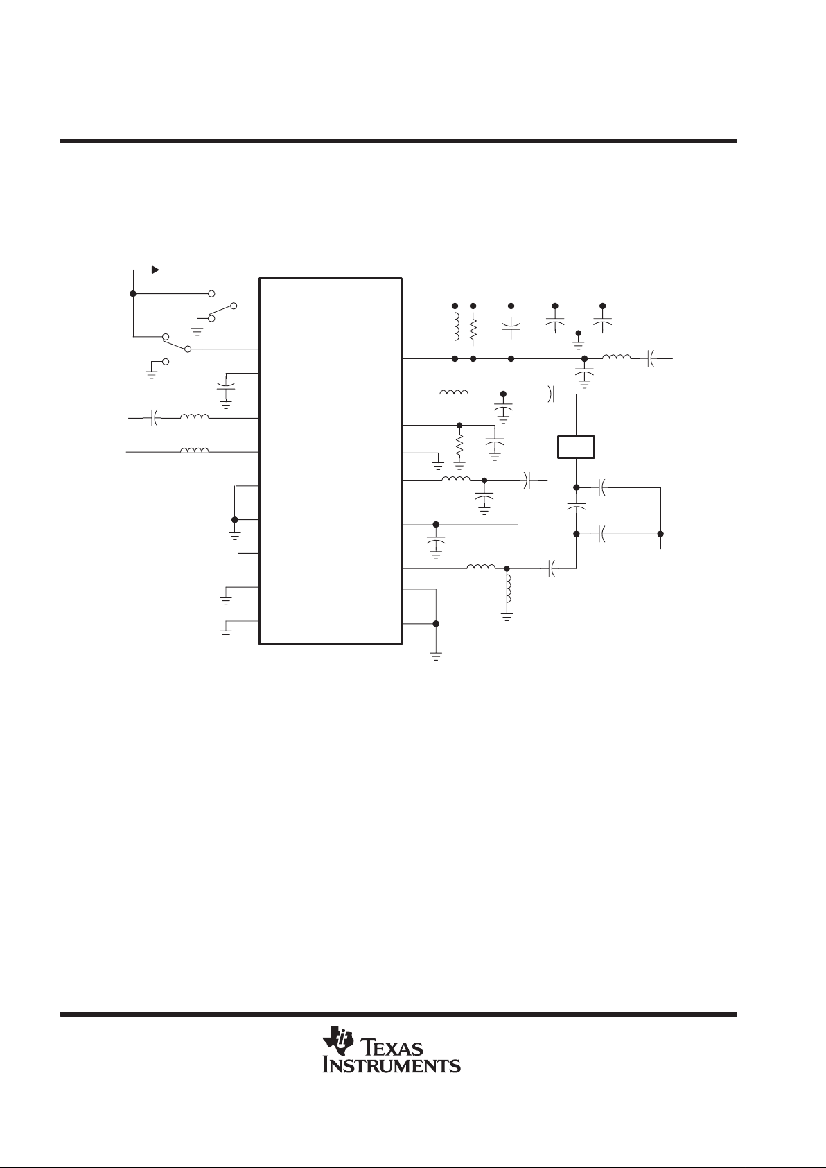
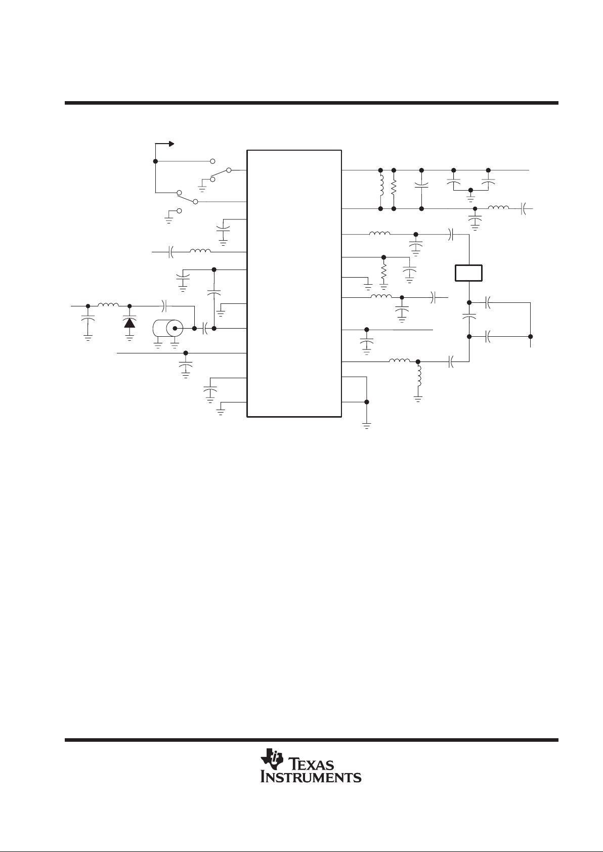
Figure 1 shows the TRF1015 configured using an external oscillator. Figure 2 shows the TRF1015 configured for an
internal oscillator. Table 2 contains a list of the component part numbers and electrical values for the components
shown in Figure 1 and Figure 2. Figure 3 through Figure 6 illustrate the typical performance for mode control when
PD1 = L and PD2 = H.
L4
C12
R1
C11
V
CC
20
19
C21
18
R2
C14
L5
L3
U2
C15
J19
L6
1
17
16
15
14
13
12
11
2
3
4
5
6
7
8
9
10
PD1
PD2
AUX_LO–
AUX_LO+
OSC2
VCO_GND
OSC1
VCO_V
CC
VCO_BYP
LNA_GND
MIX_OUT–
MIX_OUT+
MIX_IN
MIX_GND
LNA_GND
LNA_IN
LNA_V
CC
LNA_OUT
LNA_GND
LNA_GND
C10
C17
C16
C13
L8
C24
C20
V
CC
J15
C18
C23
Optional
C22
Optional
J13
2
3
1
2
3
1
V
CC
C2
C1
L1
L2
J4
J5
C19
L7
Figure 1. Recommended Application Circuit With External Oscillator
TRF1015
RF DOWNCONVERTER
SLWS021D– JUNE 1996 – REVISED JULY 1998
7
POST OFFICE BOX 655303 • DALLAS, TEXAS 75265
APPLICATION INFORMATION
L4
C12
R1
C11
V
CC
20
19
C21
18
R2
C14
L5
L3
U2
C15
J19
L6
1
17
16
15
14
13
12
11
2
3
4
PD1
PD2
AUX_LO–
AUX_LO+
MIX_OUT–
MIX_OUT+
MIX_IN
MIX_GND
LNA_GND
LNA_IN
LNA_V
CC
LNA_OUT
LNA_GND
LNA_GND
C10
C17
C16
C13
L8
C24
C20
V
CC
J15
C18
C23
Optional
C22
Optional
J13
2
3
1
2
3
1
V
CC
C2
C1
L1
J4
C19
5
6
7
8
9
10
OSC2
VCO_GND
OSC1
VCO_V
CC
VCO_BYP
LNA_GND
C5
V1
C6
L2
C9
C7
Vdc
C8
P1
C4
vco
Tune
C3
L7
Figure 2. Recommended Application Circuit With Internal Oscillator
 Loading...