
TPS780DDC
TSOT23-5
(TOPVIEW)
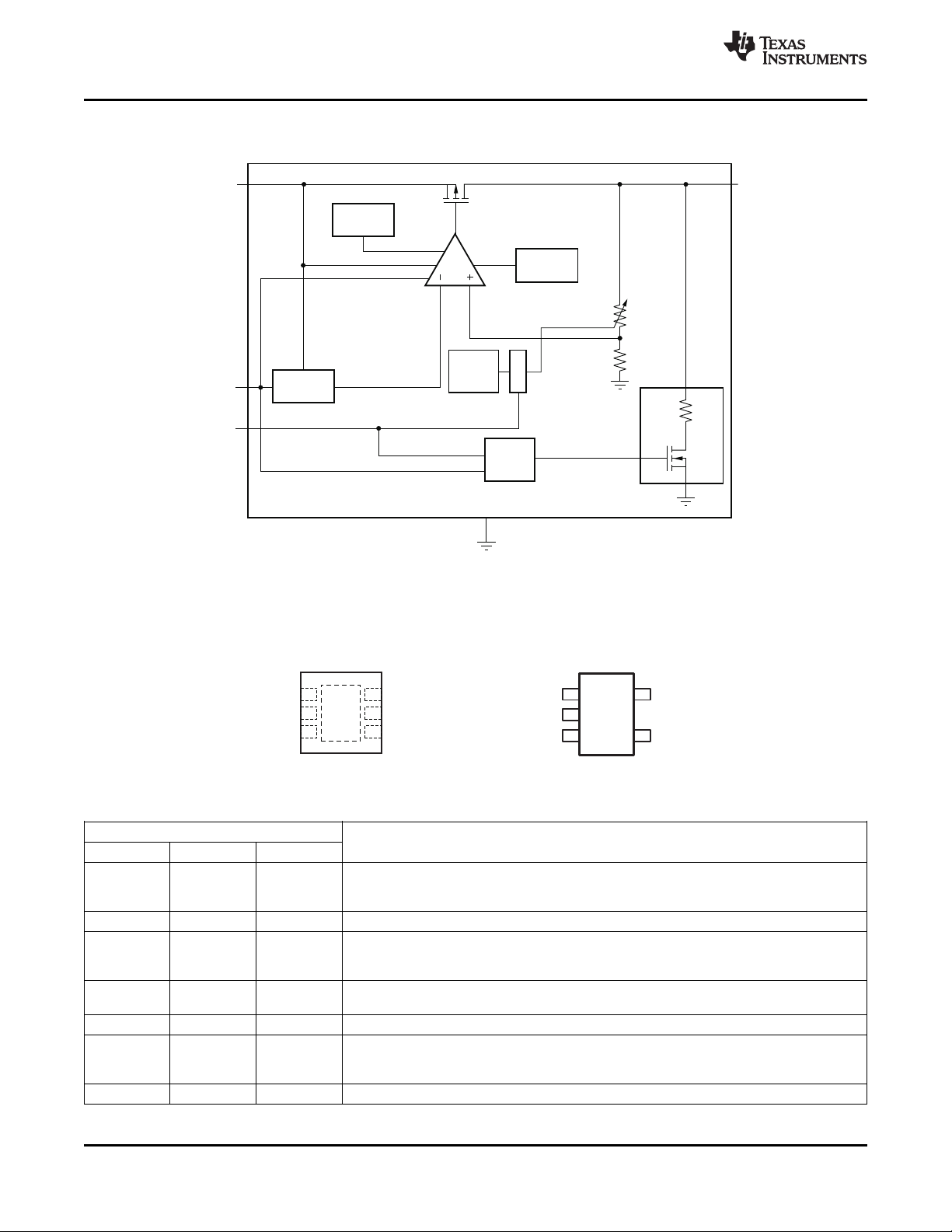
OUT
V /FB
SET
IN
GND
EN
1
2
3
5
4
TPS780DRV
2mmx2mmSON-6
(TOPVIEW)
IN
GND
EN
6
5
4
OUT
N/C
V FB/
SET
1
2
3
Thermal
Pad
TPS780 Series
www.ti.com
....................................................................................................................................................... SBVS083C – JANUARY 2007 – REVISED MAY 2008
150mA, Low-Dropout Regulator, Ultralow-Power, IQ500nA
with Pin-Selectable, Dual-Level Output Voltage
1
FEATURES
2
• Low IQ: 500nA
• 150mA, Low-Dropout Regulator with
Pin-Selectable Dual Voltage Level Output
• Low Dropout: 200mV at 150mA
• 3% Accuracy Over Load/Line/Temperature
• Available in Dual-Level, Fixed Output Voltages
from 1.5V to 4.2V Using Innovative Factory
EPROM Programming
• Available in an Adjustable Version from 1.22V
to 5.25V or a Dual-Level Output Version
• V
Pin Toggles Output Voltage Between Two
SET
Factory-Programmed Voltage Levels
• Stable with a 1.0 µ F Ceramic Capacitor
• Thermal Shutdown and Overcurrent Protection
• CMOS Logic Level-Compatible Enable Pin
• Available in DDC (TSOT23-5) or DRV (2mm ×
2mm SON-6) Package Options
The V
two voltage levels on-the-fly through a
microprocessor-compatible input. This LDO is
designed specifically for battery-powered applications
where dual-level voltages are needed. With ultralow
IQ(500nA), microprocessors, memory cards, and
smoke detectors are ideal applications for this device.
The ultralow-power and selectable dual-level output
voltages allow designers to customize power
consumption for specific applications. Designers can
now shift to a lower voltage level in a battery-powered
design when the microprocessor is in sleep mode,
further reducing overall system power consumption.
The two voltage levels are preset at the factory
through a unique architecture using an EPROM. The
EPROM technique allows for numerous output
voltage options between V
V
SET
only. Consult with your local factory representative for
exact voltage options and ordering information;
minimum order quantities may apply.
The TPS780 series are designed to be compatible
APPLICATIONS
• TI MSP430 Attach Applications
• Power Rails with Programming Mode
• Dual Voltage Levels for Power-Saving Mode
with the TI MSP430 and other similar products. The
enable pin is compatible with standard CMOS logic.
This LDO is stable with any output capacitor greater
than 1.0 µ F. Therefore, implementations of this device
require minimal board space because of miniaturized
• Wireless Handsets, Smartphones, PDAs, MP3 packaging and a potentially small output capacitor.
Players, and Other Battery-Operated Handheld The TPS780 series IQ(500nA) also come with
Products thermal shutdown and current limit to protect the
device during fault conditions. All packages have an
DESCRIPTION
operating temperature range of T
+125 ° C. For more cost-sensitive applications
The TPS780 family of low-dropout (LDO) regulators
offer the benefits of ultralow power (I
miniaturized packaging (2 × 2 SON-6), and selectable
= 500nA),
Q
requiring a dual-level voltage option and only on par
IQ, consider the TPS781 series , with an IQof 1.0 µ A
and dynamic voltage scaling.
dual-level output voltage levels. An adjustable version
is also available, but does not have the capability to
shift voltage levels.
pin allows the end user to switch between
SET
low (1.5V to 4.2V) and
SET
high (2.0V to 3.0V) in the fixed output version
J
= – 40 ° C to
1
2 All trademarks are the property of their respective owners.
PRODUCTION DATA information is current as of publication date.
Products conform to specifications per the terms of the Texas
Instruments standard warranty. Production processing does not
necessarily include testing of all parameters.
Please be aware that an important notice concerning availability, standard warranty, and use in critical applications of
Texas Instruments semiconductor products and disclaimers thereto appears at the end of this data sheet.
Copyright © 2007 – 2008, Texas Instruments Incorporated
TPS780 Series
SBVS083C – JANUARY 2007 – REVISED MAY 2008 .......................................................................................................................................................
www.ti.com
This integrated circuit can be damaged by ESD. Texas Instruments recommends that all integrated circuits be handled with
appropriate precautions. Failure to observe proper handling and installation procedures can cause damage.
ESD damage can range from subtle performance degradation to complete device failure. Precision integrated circuits may be more
susceptible to damage because very small parametric changes could cause the device not to meet its published specifications.
ORDERING INFORMATION
PRODUCT V
TPS780 vvvxxxyyyz VVV is the nominal output voltage for V
XXX is the nominal output voltage for V
YYY is the package designator.
Z is the tape and reel quantity (R = 3000, T = 250).
Adjustable version
(3) (4)
(1) (2)
OUT
OUT(HIGH)
OUT(LOW)
and corresponds to V
and corresponds to V
pin low.
SET
pin high.
SET
(1) For the most current package and ordering information see the Package Option Addendum at the end of this document, or see the TI
web site at www.ti.com .
(2) Additional output voltage combinations are available on a quick-turn basis using innovative, factory EPROM programming.
Minimum-order quantities apply; contact your sales representative for details and availability.
(3) To order the adjustable version, use TPS78001YYYZ.
(4) The device is either fixed voltage, dual-level V
output simultaneously.
ABSOLUTE MAXIMUM RATINGS
, or adjustable voltage only. Device design does not permit a fixed and adjustable
OUT
(1)
At TJ= – 40 ° C to +125 ° C, unless otherwise noted. All voltages are with respect to GND.
PARAMETER TPS780 Series UNIT
Input voltage range, V
Enable and V
SET
Output voltage range, V
Maximum output current, I
IN
voltage range, V
OUT
OUT
and V
EN
VSET
Output short-circuit duration Indefinite
Total continuous power dissipation, P
ESD rating
Human body model (HBM) 2 kV
Charged device model (CDM) 500 V
Operating junction temperature range, T
Storage temperature range, T
DISS
J
STG
(1) Stresses above these ratings may cause permanent damage. Exposure to absolute maximum conditions for extended periods may
degrade device reliability. These are stress ratings only, and functional operation of the device at these or any other conditions beyond
those specified is not implied.
(2) V
and V
EN
absolute maximum rating are VIN+ 0.3V or +6.0V, whichever is less.
VSET
– 0.3 to +6.0 V
– 0.3 to VIN+ 0.3
(2)
– 0.3 to VIN+ 0.3V V
Internally limited
See the Dissipation Ratings table
– 40 to +125 ° C
– 55 to +150 ° C
V
DISSIPATION RATINGS
BOARD PACKAGE R
(1)
High-K
(1)
High-K
DRV 20 ° C/W 65 ° C/W 15.4mW/ ° C 1540mW 845mW 615mW
DDC 90 ° C/W 200 ° C/W 5.0mW/ ° C 500mW 275mW 200mW
θ JC
R
θ JA
(1) The JEDEC high-K (2s2p) board used to derive this data was a 3-inch × 3-inch, multilayer board with 1-ounce internal power and ground
planes and 2-ounce copper traces on top and bottom of the board.
2 Submit Documentation Feedback Copyright © 2007 – 2008, Texas Instruments Incorporated
DERATING FACTOR
ABOVE TA= +25 ° C TA< +25 ° C TA= +70 ° C TA= +85 ° C
TPS780 Series
www.ti.com
....................................................................................................................................................... SBVS083C – JANUARY 2007 – REVISED MAY 2008
ELECTRICAL CHARACTERISTICS
Over operating temperature range (T
100 µ A, V
V
V
OUT
V
V
OUT_RANGE
Δ V
OUT
Δ V
OUT
V
V
V
V
I
CL
I
GND
I
SHDN
I
VSET
I
EN
I
FB
PSRR Power-supply rejection ratio V
t
TR(H → L)
t
TR(L → H)
t
STR
t
SHDN
T
T
(1) The output voltage for V
(2) Adjustable version only.
(3) No V
(4) No dynamic voltage scaling on the adjustable version.
(5) V
DO
(6) I
GND
(7) The TPS78001 FB pin is tied to V
(8) Time from V
(9) Time from V
(10) See Shutdown in the Application Information section for more details.
= V
VSET
= VIN, C
EN
OUT
PARAMETER TEST CONDITIONS MIN TYP MAX UNIT
IN
FB
Input voltage range 2.2 5.5 V
(1)
DC output accuracy
Internal reference
(adjustable version only)
Output voltage range
(adjustable version only)
/ Δ V
Line regulation V
IN
/ Δ I
DO
N
HI
LO
Load regulation 0mA ≤ I
OUT
Dropout voltage
(5)
Output noise voltage 86 µ V
V
high (output V
SET
selected), or EN high (enabled)
V
low (output V
SET
selected), or EN low (disabled)
Output current limit V
Ground pin current
Shutdown current (I
V
pin current V
SET
EN pin current V
FB pin current
(7)
(adjustable version only)
V
transition time (high-to-low) V
OUT
V
= 97% × V
SD
J
SET
OUT
V
transition time (low-to-high) V
OUT
V
= 97% × V
OUT
Startup time
Shutdown time
Thermal shutdown temperature
Operating junction temperature – 40 +125 ° C
pin on the adjustable version.
OUT(HIGH)
OUT(LOW)
(8)
(9)
= low/high is programmed at the factory.
SET
is not measured for devices with V
= 800nA (max) up to +100 ° C.
= 1.2V to V
EN
EN
= 0.4V to V
OUT
OUT
(2)
= – 40 ° C to +125 ° C), V
J
= 1.0 µ F, fixed or adjustable, unless otherwise noted. Typical values at TJ= +25 ° C.
Nominal TJ= +25 ° C, V
Over VIN, I
temperature 0mA ≤ I
(3) (4)
OUT(LOW)
OUT(HIGH)
) 18 130 nA
GND
OUT(NOM)
. Adjustable version only.
OUT
= 90% (V
= 10% (V
, V
OUT
OUT
TJ= +25 ° C, VIN= 4.0V, I
VIN= 5.5V, I
OUT(NOM)
VIN= 95% V
BW = 100Hz to 100kHz, VIN= 2.2V,
V
OUT
OUT
I
OUT
I
OUT
V
EN
TJ= – 40 ° C to +100 ° C
EN
EN
VIN= 5.5V, V
VIN= 4.3V,
OUT
I
OUT
OUT_LOW
I
OUT
OUT_HIGH
I
OUT
C
OUT
V
OUT
I
OUT
V
OUT
V
OUT(NOM)
Shutdown, temperature increasing +160 ° C
Reset, temperature decreasing +140 ° C
< 2.3V because minimum VIN= 2.2V.
OUT(NOM)
OUT(NOM)
).
).
= V
IN
OUT(NOM)
+ 0.5V or 2.2V, whichever is greater; I
=
OUT
TPS780 Series
= high/low – 2 ± 1 +2 %
SET
+ 0.5V ≤ VIN≤ 5.5V,
≤ 150mA, V
OUT
= 100 µ A
OUT
+ 0.5V ≤ VIN≤ 5.5V, I
≤ 150mA – 2 +2 %
OUT
OUT(NOM)
= 1.2V, I
= 1mA
OUT
= high/low
SET
= 75mA 1.216 V
OUT
(2)
= 5mA – 1 +1 %
OUT
, I
= 150mA 250 mV
OUT
– 3.0 ± 2.0 +3.0 %
V
1.2 V
5.25 V
FB
IN
0 0.4 V
= 0.90 × V
= 0mA
OUT(NOM)
(6)
150 230 400 mA
420 800 nA
= 150mA 5 µ A
≤ 0.4V, 2.2V ≤ VIN< 5.5V,
= V
= V
= 5.5V 70 nA
VSET
= 5.5V 40 nA
VSET
OUT
= 1.2V, I
= 100 µ A 10 nA
OUT
f = 10Hz 40 dB
= 3.3V, f = 100Hz 20 dB
= 150mA
= 2.2V, V
= 10mA
= 3.3V, V
= 10mA
= 1.0 µ F, V
= 90% V
= 150mA, C
= 90% V
OUT(NOM)
OUT(NOM)
f = 1kHz 15 dB
= 1.0 µ F, V
to V
= 3.3V,
= 2.2V,
OUT(NOM)
OUT
to
= 2.8V,
OUT
= 10% 500
800 µ s
800 µ s
500 µ s
(10)
OUT(HIGH)
OUT(LOW)
= 10% V
OUT
OUT
RMS
V
µ s
Copyright © 2007 – 2008, Texas Instruments Incorporated Submit Documentation Feedback 3
Thermal
Shutdown
10kW
Current
Limit
Bandgap
IN
EN
OUT
EPROM
MUX
V
SET
/FB
(1)
LOGIC
Active
Pull-
Down
GND
TPS780DRV
2mmx2mmSON-6
(TOPVIEW)
IN
GND
EN
6
5
4
OUT
N/C
V FB/
SET
1
2
3
Thermal
Pad
(1)
TPS780DDC
TSOT23-5
(TOPVIEW)
OUT
V /FB
SET
IN
GND
EN
1
2
3
5
4
TPS780 Series
SBVS083C – JANUARY 2007 – REVISED MAY 2008 .......................................................................................................................................................
www.ti.com
FUNCTIONAL BLOCK DIAGRAM
(1) Feedback pin (FB) for adjustable versions; V
SET
for fixed voltage versions.
PIN CONFIGURATIONS
(1) It is recommended that the SON package thermal pad be connected to ground.
Table 1. TERMINAL FUNCTIONS
TERMINAL
NAME DRV DDC DESCRIPTION
Regulated output voltage pin. A small (1 µ F) ceramic capacitor is needed from this pin to
OUT 1 5 ground to assure stability. See the Input and Output Capacitor Requirements in the
Application Information section for more details.
N/C 2 — Not connected.
Feedback pin (FB) for adjustable versions; V
V
/FB 3 4 pin (V
SET
EN 4 3
selects preset output voltage low.
) below 0.4V selects preset output voltage high. Driving the V
SET
Driving the enable pin (EN) over 1.2V turns on the regulator. Driving this pin below 0.4V puts
the regulator into shutdown mode, reducing operating current to 18nA typical.
GND 5 2 Ground pin.
IN 6 1 capacitor = 1.0 µ F. Both input and output capacitor grounds should be tied back to the IC
Thermal pad Thermal pad — It is recommended that the SON package thermal pad be connected to ground.
4 Submit Documentation Feedback Copyright © 2007 – 2008, Texas Instruments Incorporated
Input pin. A small capacitor is needed from this pin to ground to assure stability. Typical input
ground with no significant impedance between them.
for fixed voltage versions. Driving the select
SET
pin over 1.2V
SET
2.2 2.7 3.2 3.7 4.2 4.7 5.2 5.7
V (V)
IN
V (%)
OU
T
0.3
0.2
0.1
0
-0.1
-0.2
-0.3
TJ=+85°C
TJ=+25°C
T = 40- °JC
TJ=+125°C
2.7 3.2 3.7 4.2 4.7 5.2 5.7
V (V)
IN
V (%)
O
UT
1.0
0.8
0.6
0.4
0.2
0
-0.2
-0.4
-0.6
-0.8
-1.0
TJ=+125°C
T = 40- °JC
TJ=+25°C
TJ=+85°C
2.7 3.2 3.7 4.2 4.7 5.2 5.7
V (V)
IN
V (%)
OUT
3
2
1
0
-1
-2
-3
TJ=+85°C
T = 40- °JC
TJ=+25°C
3.8 4.0 4.2 4.4 4.6 4.8 5.0 5.2 5.4 5.6
V (V)
IN
V (%)
OUT
1.0
0.8
0.6
0.4
0.2
0
-0.2
-0.4
-0.6
-0.8
-1.0
T =+85°JC
T = 40- °JC
T =+25°JC
3.8 4.0 4.2 4.4 4.6 4.8 5.0 5.2 5.4 5.6
V (V)
IN
V (%)
OU
T
3
2
1
0
-1
-2
-3
TJ=+85°C
T 40- °
J
= C
TJ=+25°C
0 25 50 75 100 125 150
I (mA)
OUT
V (%)
O
UT
1.5
1.0
0.5
0
-0.5
-1.0
TJ=+125°C
TJ=+25°C
T = 40- °JC
TJ=+85°C
TPS780 Series
www.ti.com
....................................................................................................................................................... SBVS083C – JANUARY 2007 – REVISED MAY 2008
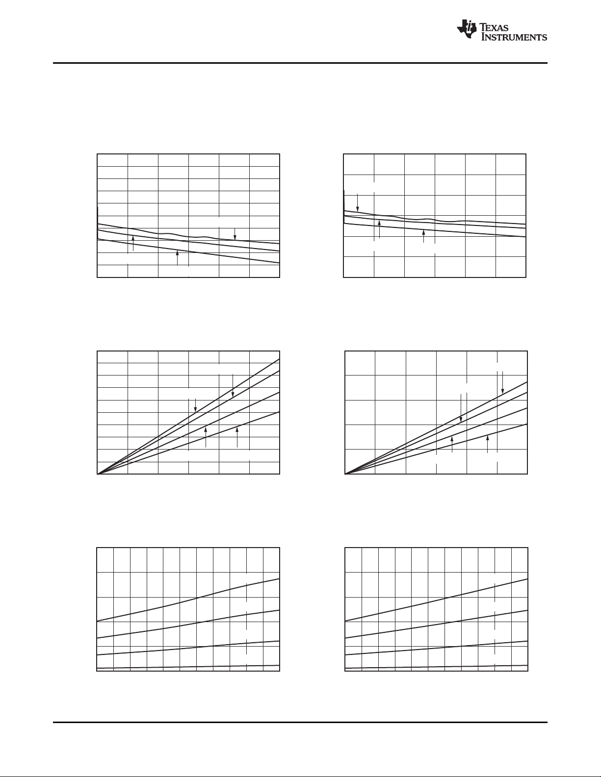
TYPICAL CHARACTERISTICS
Over the operating temperature range of TJ= – 40 ° C to +125 ° C, V
I
I
OUT
OUT
I
OUT
= 150mA, V
= 100 µ A, V
LINE REGULATION LINE REGULATION
= 5mA, V
TPS78001 TPS780330220
Figure 1. Figure 2.
LINE REGULATION LINE REGULATION
VSET
TPS780330220 TPS780330220
= V
EN
= 1.22V (typ) I
OUT
= 1.2V, V
= VIN, C
VSET
= 2.2V (typ) I
OUT
OUT
= 1 µ F, and C
= V
IN
OUT(TYP)
= 1 µ F, unless otherwise noted.
IN
= 5mA, V
OUT
= 5mA, V
OUT
+ 0.5V or 2.2V, whichever is greater;
= 1.2V, V
VSET
= 0.4V, V
VSET
OUT
OUT
= 2.2V (typ)
= 3.3V (typ)
Figure 3. Figure 4.
LINE REGULATION LOAD REGULATION
I
= 150mA, V
OUT
Copyright © 2007 – 2008, Texas Instruments Incorporated Submit Documentation Feedback 5
VSET
TPS780330220 TPS78001
Figure 5. Figure 6.
= 0.4V, V
= 3.3V (typ) V
OUT
= 3.3V
OUT
0 25 50 75 100 125 150
I (mA)
OUT
V (%)
OUT
3.0
2.5
2.0
1.5
1.0
0.5
0
-0.5
-1.0
-1.5
-2.0
TJ=+85°C
T = 40- °JC
TJ=+25°C
0 25 50 75 100 125 150
I (mA)
OUT
V (%)
OUT
3
2
1
0
-1
-2
-3
TJ=+85°C
T = 40- °JC
TJ=+25°C
0 25 50 75 100 125 150
I (mA)
OUT
V (V V-
DO IN
OUT
)(mV)
200
180
160
140
120
100
80
60
40
20
0
TJ=+85°C
T = 40- °JC
TJ=+125°C
TJ=+25°C
0 25 50 75 100 125 150
I (mA)
OUT
V (V V-
DO IN OUT
)(mV)
250
200
150
100
50
0
TJ=+125°C
TJ=+85°C
T = 40- °JC
TJ=+25°C
-40 -25 -10 1251109580655035205
Temperature( C)°
V (V V-
DO IN OUT
)(mV)
250
200
150
100
50
0
150mA
100mA
50mA
10mA
-40 -25 -10 1251109580655035205
Temperature( C)°
V (V V-
DO IN OUT
)(mV)
250
200
150
100
50
0
150mA
100mA
50mA
10mA
TPS780 Series
SBVS083C – JANUARY 2007 – REVISED MAY 2008 .......................................................................................................................................................
TYPICAL CHARACTERISTICS (continued)
Over the operating temperature range of TJ= – 40 ° C to +125 ° C, V
I
OUT
= 100 µ A, V
= V
EN
= VIN, C
VSET
= 1 µ F, and C
OUT
= 1 µ F, unless otherwise noted.
IN
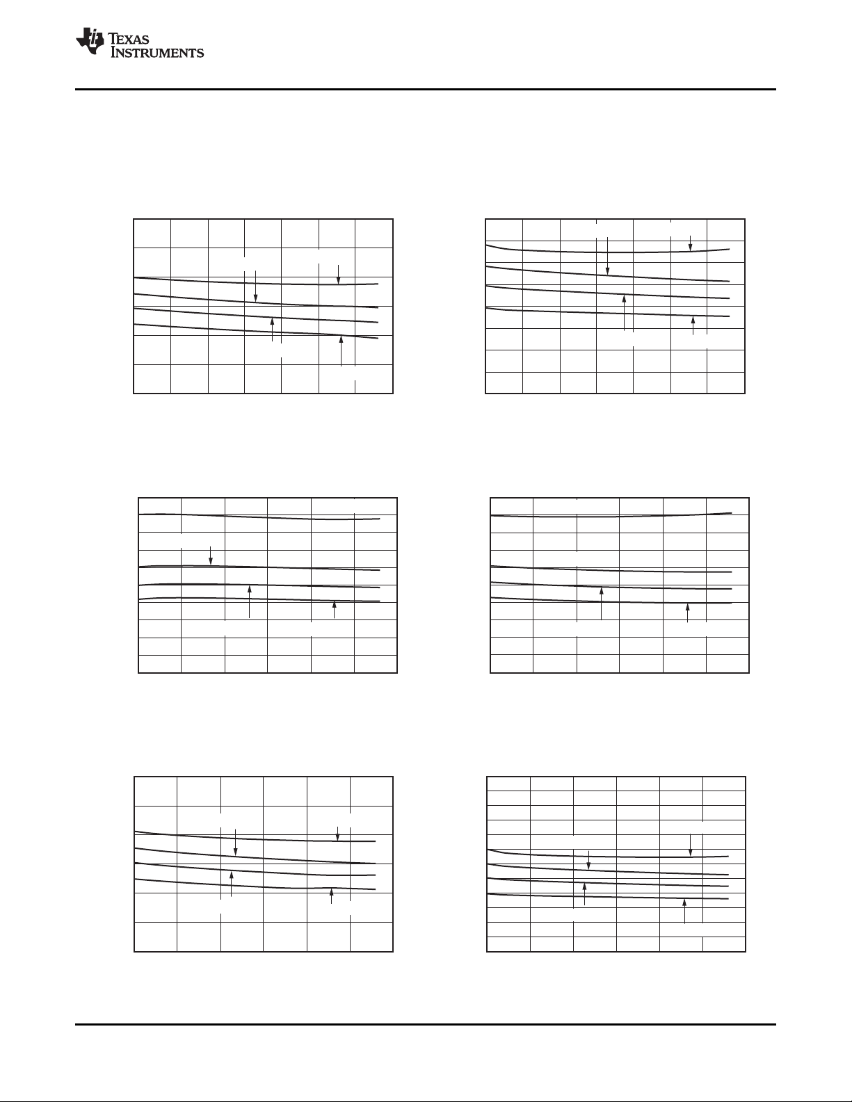
LOAD REGULATION LOAD REGULATION
V
= 1.2V, VIN= 2.7V, V
VSET
TPS780330220 TPS780330220
= 2.2V V
OUT
Figure 7. Figure 8.
DROPOUT VOLTAGE vs OUTPUT CURRENT DROPOUT VOLTAGE vs OUTPUT CURRENT
V
= 3.3V (typ), VIN= 0.95 × V
OUT
TPS78001 TPS780330220
(typ) V
OUT
www.ti.com
= V
IN
OUT(TYP)
+ 0.5V or 2.2V, whichever is greater;
= 0.4V, VIN= 3.8V, V
VSET
= 0.4V, V
VSET
OUT
= 3.3V
OUT
= 3.3V (typ), VIN= 0.95 × V
(typ)
OUT
DROPOUT VOLTAGE vs TEMPERATURE DROPOUT VOLTAGE vs TEMPERATURE
V
= 3.3V (typ), VIN= 0.95 × V
OUT
6 Submit Documentation Feedback Copyright © 2007 – 2008, Texas Instruments Incorporated
Figure 9. Figure 10.
(typ) V
TPS78001 TPS780330220
OUT
= 0.4V, V
VSET
= 3.3V (typ), VIN= 0.95 × V
OUT
Figure 11. Figure 12.
(typ)
OUT
2.2 2.7 3.2 3.7 4.2 4.7 5.2 5.7
V (V)
IN
I A)m
GND
(
6
5
4
3
2
1
0
T C°
J
=+125
T C°
J
=+85
T = 40- °JC
T C°
J
=+25
2.2 2.7 3.2 3.7 4.2 4.7 5.2 5.7
V (V)
IN
I
(
A)m
GND
8
7
6
5
4
3
2
1
0
T =+125 C°
J
T =+85 C°
J
TJ= 40- °C
T =+25 C°
J
2.7 3.2 3.7 4.2 4.7 5.2 5.7
V (V)
IN
I (nA)
GN
D
1000
900
800
700
600
500
400
300
200
100
0
TJ=+125°C
TJ=+85°C
TJ= 40- °C
TJ=+25°C
2.7 3.2 3.7 4.2 4.7 5.2 5.7
V (V)
IN
I (nA)
GN
D
1000
900
800
700
600
500
400
300
200
100
0
T =+125 C°
J
T =+85 C°
J
T = 40- °JC
T =+25 C°
J
2.7 3.2 3.7 4.2 4.7 5.2 5.7
V (V)
IN
I ( A)m
GND
6
5
4
3
2
1
0
T =+125 C°
J
T =+85 C°
J
T 40- °
J
= C
T =+25 C°
J
2.7 3.2 3.7 4.2 4.7 5.2 5.7
V (V)
IN
I ( A)m
GN
D
12
11
10
9
8
7
6
5
4
3
2
1
0
T =+125 CJ°
T =+85 CJ°
T = 40- °JC
T =+25 CJ°
TPS780 Series
www.ti.com
....................................................................................................................................................... SBVS083C – JANUARY 2007 – REVISED MAY 2008
TYPICAL CHARACTERISTICS (continued)
Over the operating temperature range of TJ= – 40 ° C to +125 ° C, V
I
OUT
= 100 µ A, V
= V
EN
= VIN, C
VSET
= 1 µ F, and C
OUT
= 1 µ F, unless otherwise noted.
IN
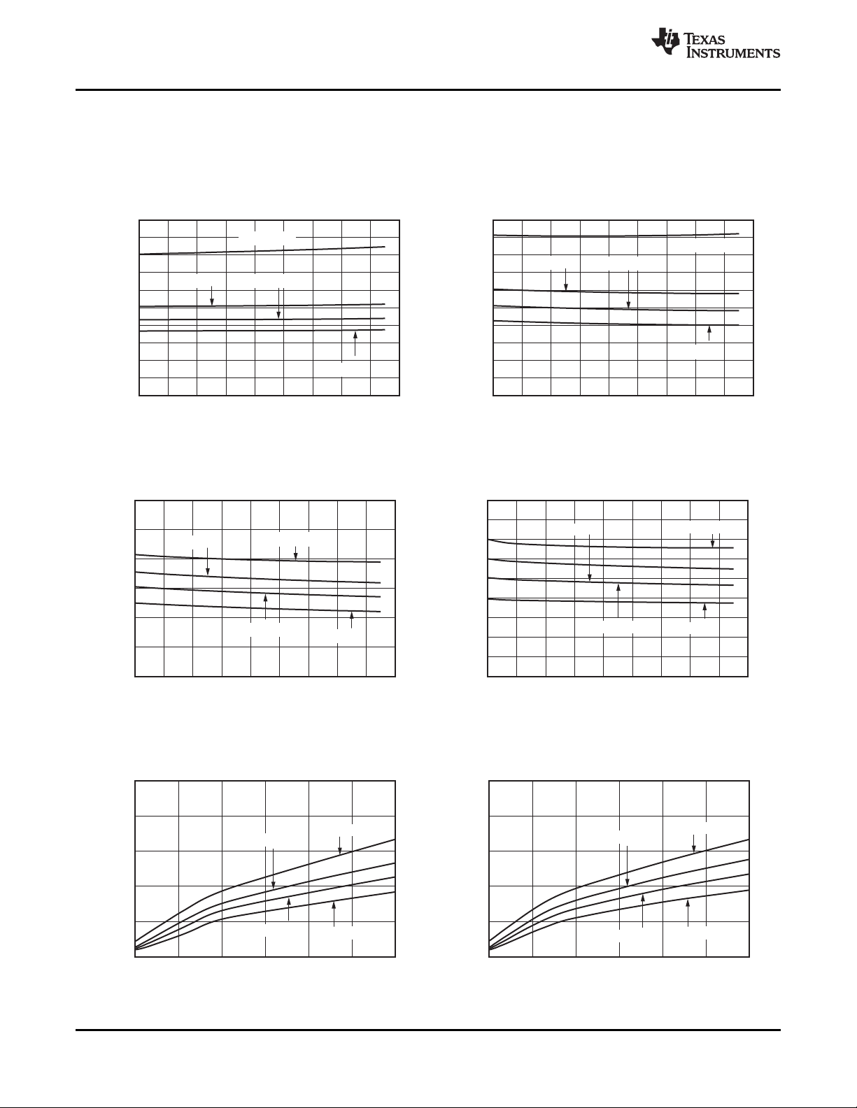
GROUND PIN CURRENT vs INPUT VOLTAGE GROUND PIN CURRENT vs INPUT VOLTAGE
I
= 50mA, V
OUT
TPS78001 TPS78001
= 1.22V I
OUT
Figure 13. Figure 14.
GROUND PIN CURRENT vs INPUT VOLTAGE GROUND PIN CURRENT vs INPUT VOLTAGE
I
OUT
= 0mA, V
= 1.2V, V
VSET
TPS780330220 TPS780330220
= 2.2V I
OUT
= V
IN
OUT(TYP)
+ 0.5V or 2.2V, whichever is greater;
= 150mA, V
OUT
OUT
= 1mA, V
= 1.2V, V
VSET
= 1.22V
OUT
= 2.2V
OUT
Figure 15. Figure 16.
GROUND PIN CURRENT vs INPUT VOLTAGE GROUND PIN CURRENT vs INPUT VOLTAGE
I
= 50mA, V
OUT
Copyright © 2007 – 2008, Texas Instruments Incorporated Submit Documentation Feedback 7
VSET
TPS780330220 TPS780330220
Figure 17. Figure 18.
= 1.2V, V
= 2.2V I
OUT
OUT
= 150mA, V
= 1.2V, V
VSET
= 2.2V
OUT
3.8 4.0 4.2 4.4 4.6 4.8 5.0 5.2 5.4 5.6
V (V)
IN
I
(nA)
GND
1000
900
800
700
600
500
400
300
200
100
0
T =+125 C°
J
T =+85 C°
J
TJ= 40- °C
T =+25 C°
J
3.8 4.0 4.2 4.4 4.6 4.8 5.0 5.2 5.4 5.6
V (V)
IN
I
(nA)
GND
1000
900
800
700
600
500
400
300
200
100
0
T °
J
=+125 C
T °
J
=+85 C
TJ= 40- °C
T °
J
=+25 C
3.8 4.0 4.2 4.4 4.6 4.8 5.0 5.2 5.4 5.6
V (V)
IN
I
(
A)m
GND
6
5
4
3
2
1
0
T =+125 C°
J
T =+85 C°
J
T 40- °
J
= C
T =+25 C°
J
3.8 4.0 4.2 4.4 4.6 4.8 5.0 5.2 5.4 5.6
V (V)
IN
I
( A)m
GND
9
8
7
6
5
4
3
2
1
0
T =+125 C°
J
T =+85 C°
J
TJ= -40°C
T =+25 C°
J
0 25 50 75 100 125 150
I (mA)
OUT
I ( A)m
GND
10
8
6
4
2
0
T =+125 C°
J
T =+85 C°
J
T = 40- °JC
T =+25 C°
J
0 25 50 75 100 125 150
I (mA)
OUT
I ( A)m
GND
10
8
6
4
2
0
T =+125 C°
J
T =+85 C°
J
TJ= 40- °C
T =+25 C°
J
TPS780 Series
SBVS083C – JANUARY 2007 – REVISED MAY 2008 .......................................................................................................................................................
TYPICAL CHARACTERISTICS (continued)
Over the operating temperature range of TJ= – 40 ° C to +125 ° C, V
I
OUT
= 100 µ A, V
= V
EN
= VIN, C
VSET
= 1 µ F, and C
OUT
= 1 µ F, unless otherwise noted.
IN
GROUND PIN CURRENT vs INPUT VOLTAGE GROUND PIN CURRENT vs INPUT VOLTAGE
I
OUT
= 0mA, V
= 0.4V, V
VSET
TPS780330220 TPS780330220
= 3.3V I
OUT
Figure 19. Figure 20.
GROUND PIN CURRENT vs INPUT VOLTAGE GROUND PIN CURRENT vs INPUT VOLTAGE
I
OUT
= 50mA, V
= 0.4V, V
VSET
TPS780330220 TPS780330220
= 3.3V I
OUT
www.ti.com
= V
IN
OUT(TYP)
+ 0.5V or 2.2V, whichever is greater;
OUT
OUT
= 1mA, V
= 150mA, V
= 0.4V, V
VSET
= 0.4V, V
VSET
= 3.3V
OUT
= 3.3V
OUT
Figure 21. Figure 22.
GROUND PIN CURRENT vs OUTPUT CURRENT GROUND PIN CURRENT vs OUTPUT CURRENT
V
= 1.2V, VIN= 5.5V, V
VSET
8 Submit Documentation Feedback Copyright © 2007 – 2008, Texas Instruments Incorporated
TPS780330220 TPS780330220
Figure 23. Figure 24.
= 2.2V V
OUT
= 0.4V, VIN= 5.5V, V
VSET
= 3.3V
OUT
 Loading...