

TPS74301
TPS74301
www.ti.com
R
1
R
5
R
3
R
4
R
2
V
OUT
C
OUT
Optional
PG
OUT
FB
IN
BIAS
TRACK
GND
V
IN
V
BIAS
C
IN
C
BIAS
V
TRACK
V
PG
TPS74301
EN
500mV/div
Time(20ms/div)
V
PG
V
TRACK
I =500mA
OUT
V
OUT
1.5A Ultra-LDO with Programmable Sequencing
TPS74301
SBVS065E – DECEMBER 2005 – REVISED MAY 2007
FEATURES
• Track Pin Allows for Flexible Power-Up
Sequencing
• 1% Accuracy Over Line, Load, and
Temperature
• Supports Input Voltages as Low as 0.9V with
External Bias Supply
• Adjustable Output (0.8V to 3.6V)
• Ultra-Low Dropout: 55mV at 1.5A (typ)
• Stable with Any or No Output Capacitor
• Excellent Transient Response
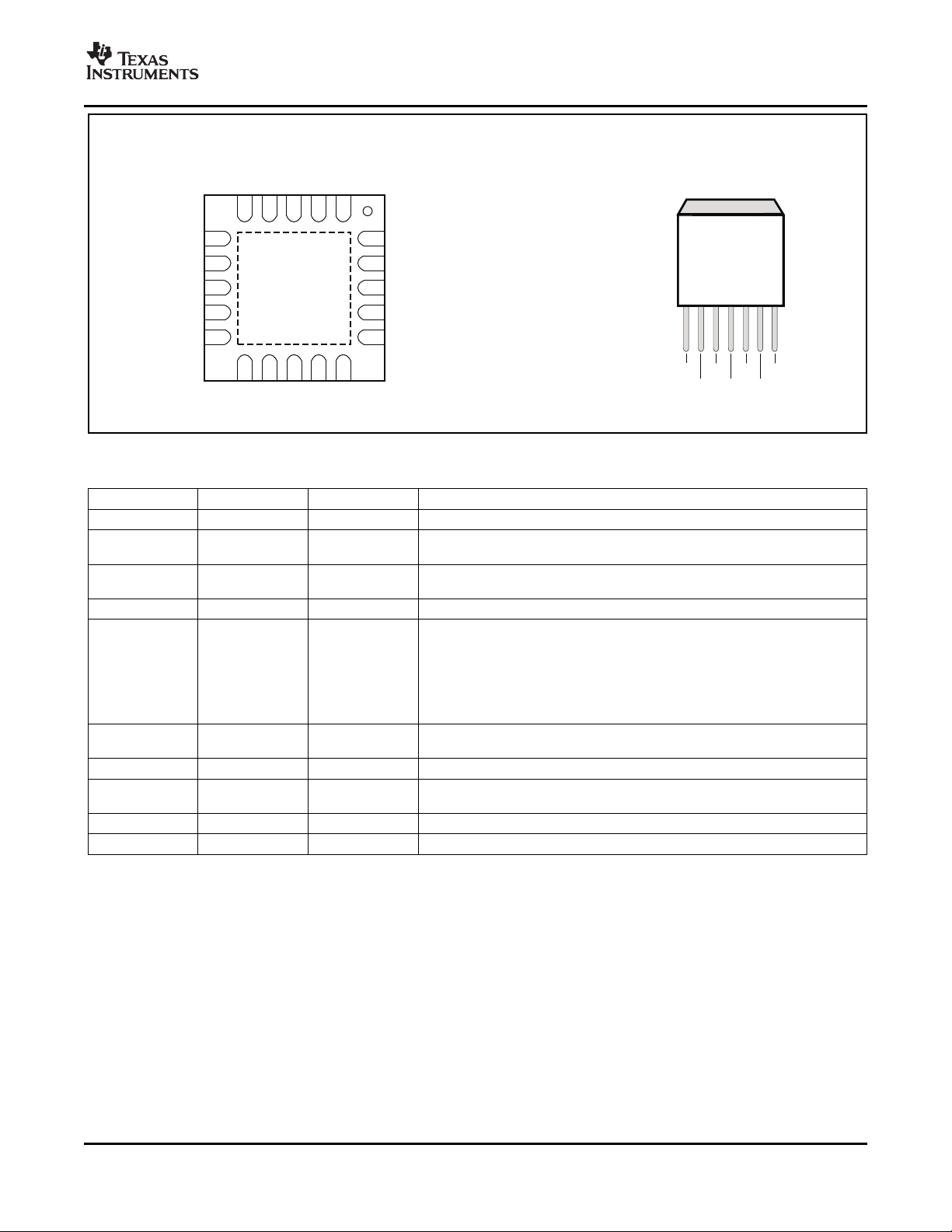
• Available in 5mm × 5mm × 1mm QFN and
DDPAK-7 Packages
• Open-Drain Power-Good (5 × 5 QFN)
• Active High Enable
APPLICATIONS
• FPGA Applications
• DSP Core and I/O Voltages
• Post-Regulation Applications
• Applications with Special Start-Up Time or
Sequencing Requirements
DESCRIPTION
The TPS74301 low-dropout (LDO) linear regulator
provides an easy-to-use robust power management
solution for a wide variety of applications. The
TRACK pin allows the output to track an external
supply. This feature is useful in minimizing the stress
on ESD structures that are present between the
CORE and I/O power pins of many processors. The
enable input and power-good output allow easy
sequencing with external regulators. This complete
flexibility allows the user to configure a solution that
meets the sequencing requirements of FPGAs,
DSPs, and other applications with special start-up
requirements.
A precision reference and error amplifier deliver 1%
accuracy over load, line, temperature, and process.
Each LDO is stable with low-cost ceramic output
capacitors and the device is fully specified from
–40 ° C to +125 ° C. The TPS74301 is offered in a
small (5mm × 5mm) QFN package, yielding a highly
compact total solution size. For applications that
require additional power dissipation, the DDPAK
(KTW) package is also available.
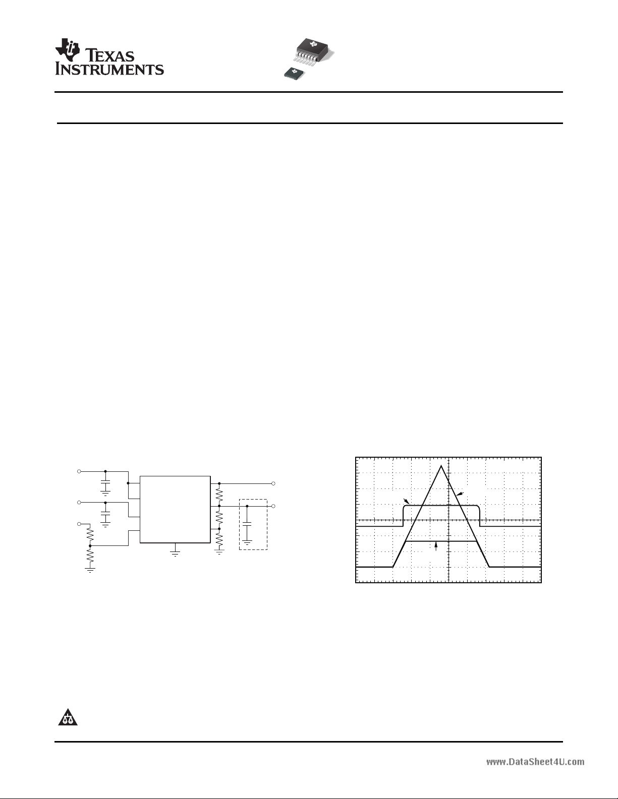
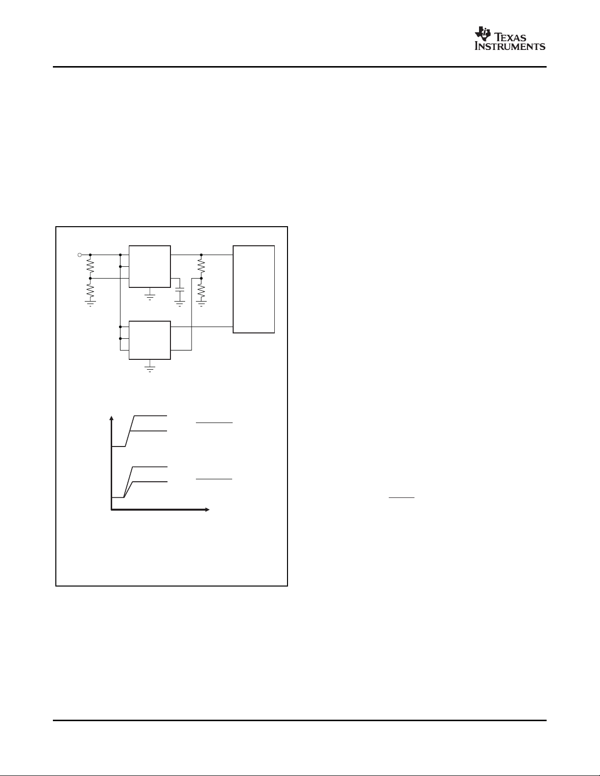
Figure 1. Typical Application Circuit
All trademarks are the property of their respective owners.
PRODUCTION DATA information is current as of publication date.
Products conform to specifications per the terms of the Texas
Instruments standard warranty. Production processing does not
necessarily include testing of all parameters.
Please be aware that an important notice concerning availability, standard warranty, and use in critical applications of Texas
Instruments semiconductor products and disclaimers thereto appears at the end of this data sheet.
Figure 2. Tracking Response
Copyright © 2005–2007, Texas Instruments Incorporated
www.ti.com
TPS74301
SBVS065E – DECEMBER 2005 – REVISED MAY 2007
This integrated circuit can be damaged by ESD. Texas Instruments recommends that all integrated circuits be handled with
appropriate precautions. Failure to observe proper handling and installation procedures can cause damage.
ESD damage can range from subtle performance degradation to complete device failure. Precision integrated circuits may be
more susceptible to damage because very small parametric changes could cause the device not to meet its published
specifications.
ORDERING INFORMATION
PRODUCT V
TPS743 xxyyyz XX is nominal output voltage (for example, 12 = 1.2V, 15 = 1.5V, 01 = Adjustable).
(1)
(2)
OUT
(3)
YYY is package designator.
Z is package quantity.
(1) For the most current package and ordering information see the Package Option Addendum at the end of this document, or see the TI
website at www.ti.com .
(2) Output voltages from 0.9V to 1.5V in 50mV increments and 1.5V to 3.3V in 100mV increments are available through the use of
innovative factory EEPROM programming; minimum order quantities may apply. Contact factory for details and availability.
(3) For fixed 0.8V operation, tie FB to OUT.
ABSOLUTE MAXIMUM RATINGS
(1)
At TJ= –40 ° C to +125 ° C, unless otherwise noted. All voltages are with respect to GND.
TPS74301 UNIT
VIN, V
V
(1) Stresses beyond those listed under Absolute Maximum Ratings may cause permanent damage to the device. These are stress ratings
only and functional operation of the device at these conditions is not implied. Exposure to absolute-maximum-rated conditions for
extended periods may affect device reliability.
Input voltage range –0.3 to +6 V
BIAS
V
Enable voltage range –0.3 to +6 V
EN
V
Power-good voltage range –0.3 to +6 V
PG
IPGPG sink current 0 to +1.5 mA
Track pin voltage range –0.3 to +6 V
TRACK
V
Feedback pin voltage range –0.3 to +6 V
FB
V
Output voltage range –0.3 to VIN+ 0.3 V
OUT
I
Maximum output current Internally limited
OUT
Output short circuit duration Indefinite
P
Continuous total power dissipation See Dissipation Ratings Table
DISS
TJOperating junction temperature range –40 to +125 ° C
T
Storage junction temperature range –55 to +150 ° C
STG
DISSIPATION RATINGS
PACKAGE θ
RGW (QFN)
KTW (DDPAK)
(1) See Figure 31 for PCB layout description.
(2) See Figure 34 for PCB layout description.
2
(1)
(2)
JA
36.5 ° C/W 4.05 ° C/W 2.74W 27.4mW/ ° C
18.8 ° C/W 2.32 ° C/W 5.32W 53.2mW/ ° C
θ
JC
POWER RATING ABOVE TA= +25 ° C
Submit Documentation Feedback
TA< +25 ° C DERATING FACTOR
www.ti.com
ELECTRICAL CHARACTERISTICS
At V
= 1.1V, V
EN
unless otherwise noted. Typical values are at TJ= +25 ° C.
V
IN
V
BIAS
V
REF
V
OUT
V
/V
OUT
IN
V
/I
OUT
OUT
V
DO
ICLCurrent limit V
I
BIAS
I
SHDN
IFBFeedback pin current
PSRR
Noise Output noise voltage 100Hz to 100kHz, I
V
TRAN
t
STR
T
ACC
ITRTrack pin current V
V
EN, HI
V
EN, LO
V
EN, HYS
V
EN, DG
IENEnable pin current V
V
IT
V
HYS
V
PG, LO
I
PG, LKG
T
J
T
SD
= V
OUT
+ 0.3V, C
IN
= C
IN
BIAS
= 0.1 µ F, C
PARAMETER TEST CONDITIONS MIN TYP MAX UNIT
Input voltage range V
Bias pin voltage range 2.375 5.25 V
Internal reference (Adj.) TJ= +25 ° C 0.796 0.8 0.804 V
Output voltage range VIN= 5V, I
BIAS
IN
IN
BIAS
dropout voltage
)
to V
OUT
(1)
)
OUT
to V
OUT
droop during load
2.375V ≤ V
V
OUT (NOM)
V
OUT (NOM)
0mA ≤ I
50mA ≤ I
I
= 1.5A, V
(2)
OUT
I
= 1.5A, V
OUT
(2)
I
= 1.5A, VIN= V
OUT
= 80% × V
OUT
= 0mA to 1.5A 2 4 mA
OUT
V
≤ 0.4V 1 100 µ A
EN
(3)
I
= 50mA to 1.5A –250 68 250 nA
OUT
1kHz, I
800kHz, I
1kHz, I
)
800kHz, I
I
= 50mA to 1.5A at 1A/ µ s, C
OUT
TRACK
Accuracy
Line regulation %/V
Load regulation
VINdropout voltage
V
Bias pin current I
Shutdown supply current
(V
Power-supply rejection
(V
Power-supply rejection
(V
%V
transient
Minimum startup time V
Track pin accuracy 0.2V ≤ V
TRACK
= 1.5A, V
OUT
≤ 5.25V, 50mA ≤ I
BIAS
+ 0.3 ≤ VIN≤ 5.5V, QFN 0.0005 0.05
+ 0.3 ≤ VIN≤ 5.5V, DDPAK 0.0005 0.06
≤ 50mA 0.013 %/mA
OUT
≤ 1.5A 0.04 %/A
OUT
BIAS
BIAS
OUT (NOM)
= 1.5A, VIN= 1.8V, V
OUT
= 1.5A, VIN= 1.8V, V
OUT
= 1.5A, VIN= 1.8V, V
OUT
= 1.5A, VIN= 1.8V, V
OUT
> 0.8V 40 µ s
≤ 0.7V, V
TRACK
= 0.4V 0.1 1 µ A
Enable input high level 1.1 5.5 V
Enable input low level 0 0.4 V
Enable pin hysteresis 50 mV
Enable pin deglitch time 20 µ s
= 5V 0.1 1 µ A
EN
PG trip threshold V
decreasing 86.5 90 93.5 %V
OUT
PG trip hysteresis 3 %V
PG output low voltage IPG= 1mA (sinking), V
PG leakage current V
PG
= 5.25V, V
OUT
Operating junction
temperature
Thermal shutdown
temperature
Shutdown, temperature increasing +155
Reset, temperature decreasing +140
SBVS065E – DECEMBER 2005 – REVISED MAY 2007
= 10 µ F, I
OUT
= 5V V
BIAS
– V
OUT (NOM)
– V
OUT (NOM)
BIAS
≥ 1.62V, QFN 55 100
≥ 1.62V, DDPAK 60 120
= 50mA, V
OUT
≤ 1.5A –1 ± 0.2 1 %
OUT
= 5.0V, and TJ= –40 ° C to +125 ° C,
BIAS
+ V
OUT
REF
1.8 4 A
= 1.5V 73
OUT
= 1.5V 42
OUT
= 1.5V 67
OUT
= 1.5V 50
OUT
= 1.5A 25 × V
OUT
= none 3.5 %V
OUT
= 0.8V –60 60 mV
OUT
< V
OUT
IT
> V
IT
–40 +125 ° C
TPS74301
TPS74301
DO
OUT
0.3 1 µ A
5.5 V
3.6 V
1.4 V
0.3 V
mV
dB
dB
µ V
RMS
OUT
OUT
OUT
° C
(1) Adjustable devices tested at 0.8V; external resistor tolerance is not taken into account.
(2) Dropout is defined as the voltage from the input to V
(3) IFBcurrent flow is out of the device.
when V
OUT
OUT
Submit Documentation Feedback
is 2% below nominal.
3
www.ti.com
Thermal
Limit
FB
PG
IN
BIAS
TRACK
EN
Hysteresis
andDe-Glitch
Current
Limit
UVLO
0.8V
Reference
0.9 V´
REF
GND
V <V =1,V >V =0
TRACK REF TRACK REF
V
OUT
R
1
R
2
V =0.8x( )
OUT
1+
R
1
R
2
1
0
TPS74301
SBVS065E – DECEMBER 2005 – REVISED MAY 2007
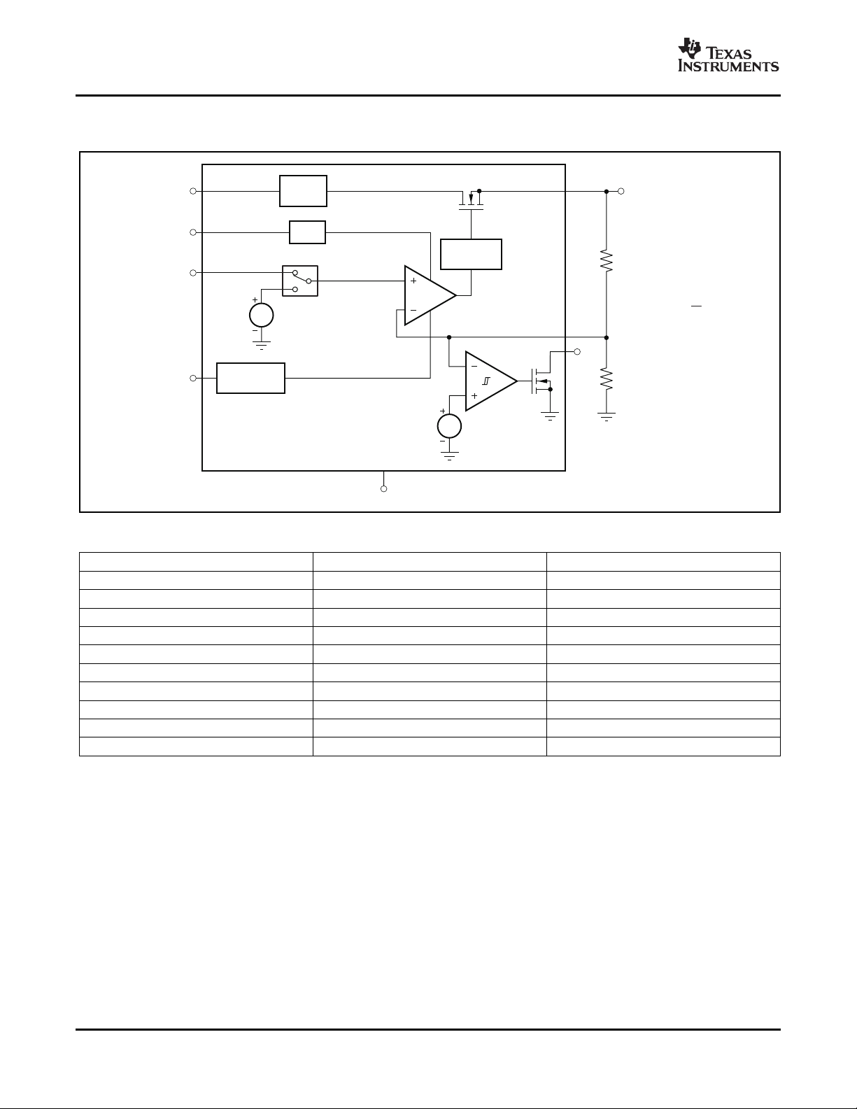
BLOCK DIAGRAM
(1) V
OUT
= 0.8 × (1 + R1/R2)
Table 1. Standard 1% Resistor Values for Programming the Output Voltage
R1(k Ω ) R2(k Ω ) V
Short Open 0.8
0.619 4.99 0.9
1.13 4.53 1.0
1.37 4.42 1.05
1.87 4.99 1.1
2.49 4.99 1.2
4.12 4.75 1.5
3.57 2.87 1.8
3.57 1.69 2.5
3.57 1.15 3.3
(1)
(V)
OUT
4
Submit Documentation Feedback
www.ti.com
IN
IN
IN
PG
BIAS
OUT
OUT
OUT
NC
FB
TPS74301
IN
EN
11
GND
12
NC
13
NC
14
TRACK
15
6
7
8
9
10
20
19
18
17
16
5
NC4
NC3
NC2
OUT1
5 5QFN(RGW)´
Package TopView¾
7-Lead
DDPAK(KTW)
Surface-Mount
OUT
GND
BIAS
IN
FB
TRACK
1 2 3 4
5
6
EN
7
TPS74301
SBVS065E – DECEMBER 2005 – REVISED MAY 2007
PIN DESCRIPTIONS
NAME KTW (DDPAK) RGW (QFN) DESCRIPTION
IN 5 5–8 Unregulated input to the device.
EN 7 11
TRACK 1 15
Enable pin. Driving this pin high enables the regulator. Driving this pin low puts
the regulator into shutdown mode. This pin must not be left floating.
Tracking pin. Connect this pin to the center tap of a resistor divider off of an
external supply to program the device to track an external supply.
BIAS 6 10 Bias input voltage for error amplifier, reference, and internal control circuits.
Power-Good (PG) is an open-drain, active-high output that indicates the status
of V
. When V
OUT
high-impedance state. When V
PG N/A 9 low-impedance state. A pull-up resistor from 10k Ω to 1M Ω should be
exceeds the PG trip threshold, the PG pin goes into a
OUT
OUT
connected from this pin to a supply up to 5.5V. The supply can be higher than
the input voltage. Alternatively, the PG pin can be left floating if output
monitoring is not necessary.
FB 2 16
This pin is the feedback connection to the center tap of an external resistor
divider network that sets the output voltage. This pin must not be left floating.
OUT 3 1, 18–20 Regulated output voltage. No capacitor is required on this pin for stability.
NC N/A 2–4, 13, 14, 17
No connection. This pin can be left floating or connected to GND to allow better
thermal contact to the top-side plane.
GND 4 12 Ground
PAD/TAB Should be soldered to the ground plane for increased thermal performance.
is below this threshold the pin is driven to a
Submit Documentation Feedback
5
www.ti.com
1.0
0.9
0.8
0.7
0.6
0.5
0.4
0.3
0.2
0.1
0
-0.1
0
10 20 30 40
ChangeinV (%)
OUT
I (mA)
OUT
50
+125 C°
+25 C°
-40 C°
ReferredtoI =50mA
OUT
0.050
0.025
0
-0.025
-0.050
-0.075
-0.100
-0.125
-0.150
50
500 1000
ChangeinV (%)
OUT
I (mA)
OUT
1500
+125 C°
+25 C°
- °40 C
ReferredtoI =50mA
OUT
0.05
0.04
0.03
0.02
0.01
0
-0.01
-0.02
-0.03
-0.04
-0.05
0
0.5 1.0 1.5 2.0 2.5 3.0 3.5 4.0
ChangeinV (%)
OUT
V V-
IN OUT
(V)
4.5
T = 40- °JC
TJ=+25°C
TJ=+125°C
100
75
50
25
0
0
0.5 1.0
DropoutVoltage(mV)
I (A)
OUT
1.5
+125 C°
+25 C°
- °40 C
200
180
160
140
120
100
80
60
40
20
0
0.9
1.4 1.9 2.4 2.9 3.4
DropoutVoltage(mV)
V V-
BIAS OUT
(V)
3.9
+125 C°
+25 C°
-40°C
I =1.5A
OUT
60
50
40
30
20
10
0
0.9
1.4 1.9 2.4 2.9 3.4
DropoutV
oltage(mV)
V -
BIASVOUT
(V)
3.9
+125 C°
+25 C°
-40°C
I =500mA
OUT
TPS74301
SBVS065E – DECEMBER 2005 – REVISED MAY 2007
At TJ= +25 ° C, V
unless otherwise noted.
= 1.5V, VIN= V
OUT
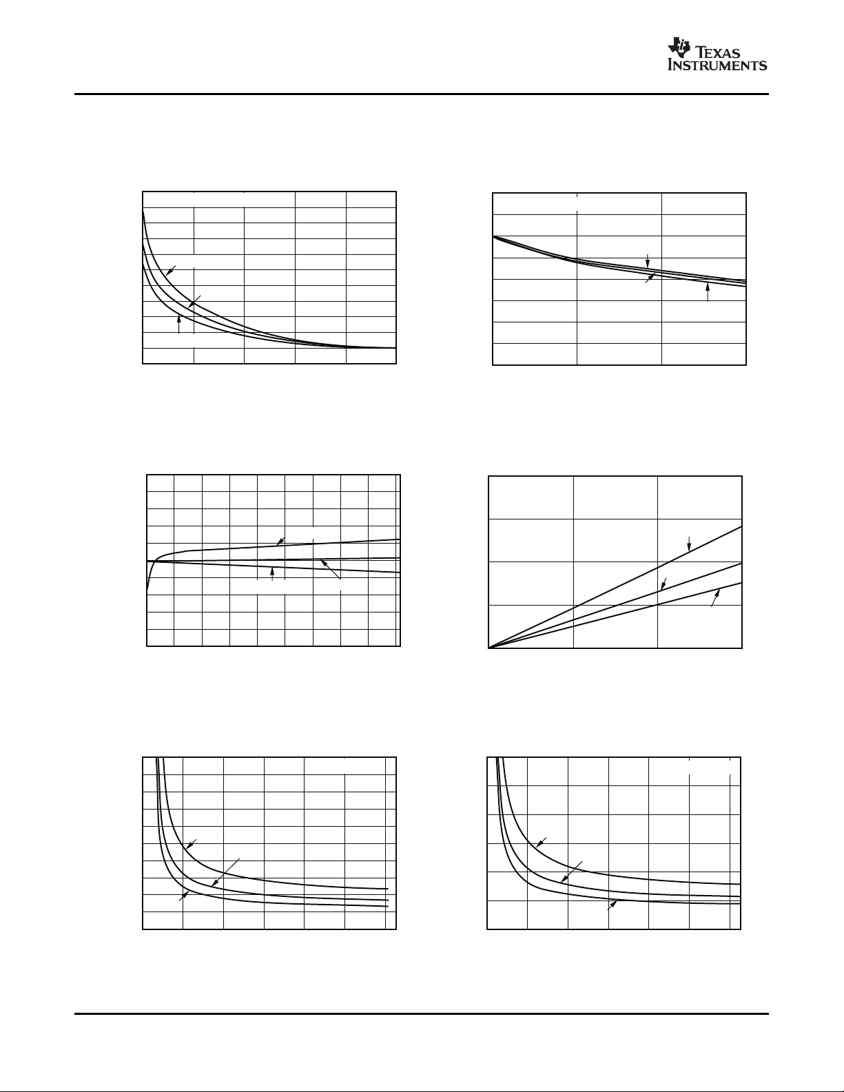
LOAD REGULATION LOAD REGULATION
Figure 3. Figure 4.
TYPICAL CHARACTERISTICS
OUT(TYP)
+ 0.3V, V
BIAS
= 3.3V, I
= 50mA, EN = VIN, CIN= 1 µ F, C
OUT
= 4.7 µ F, and C
BIAS
= 10 µ F,
OUT
LINE REGULATION I
AND TEMPERATURE (TJ)
OUT
Figure 5. Figure 6.
VINDROPOUT VOLTAGE vs VINDROPOUT VOLTAGE vs
V
– V
VINDROPOUT VOLTAGE vs
BIAS
AND TEMPERATURE (TJ) V
OUT
– V
BIAS
AND TEMPERATURE (TJ)
OUT
6
Figure 7. Figure 8.
Submit Documentation Feedback
www.ti.com
1400
1300
1200
1100
1000
900
800
700
600
500
50
500 1000
DropoutVoltage(mV)
I (mA)
OUT
1500
+125 C°
+25 C°
- °40 C
90
80
70
60
50
40
30
20
10
0
P
ower
-SupplyRejection(dB)
10 100
1k
10k 100k
1M
10M
Frequency(Hz)
I =1.5A
OUT
100
90
80
70
60
50
40
30
20
10
0
10
100 1k 10k 100k 1M
Power
-SupplyRejectionRatio(dB)
Frequency(Hz)
10M
V =1.8,V =1.5V
IN OUT OUT
,I =1.5A
C =0 F
OUT
m
C =10 F
OUT
m
C =100 F
OUT
m
100
90
80
70
60
50
40
30
20
10
0
10
100 1k 10k 100k 1M
Power
-SupplyRejectionRatio(dB)
Frequency(Hz)
10M
V =1.8,V =1.5V
IN OUT OUT
,I =100mA
C =10 F
OUT
m
C =100 F
OUT
m
C =0 F
OUT
m
90
80
70
60
50
40
30
20
10
0
0
0.25 0.50 0.75 1.00 1.25 1.50 1.75 2.00 2.25
Power-SupplyRejectionRatio(dB)
V V-
IN OUT
(V)
2.50
1kHz
100kHz
300kHz
700kHz
I =1.5A
OUT
1
0.1
0.01
100
1k 10k
OutputSpectralNoiseDensity(mV/Ö
)
Hz
Frequency(Hz)
100k
I =1.5A
OUT
V =1.1V
OUT
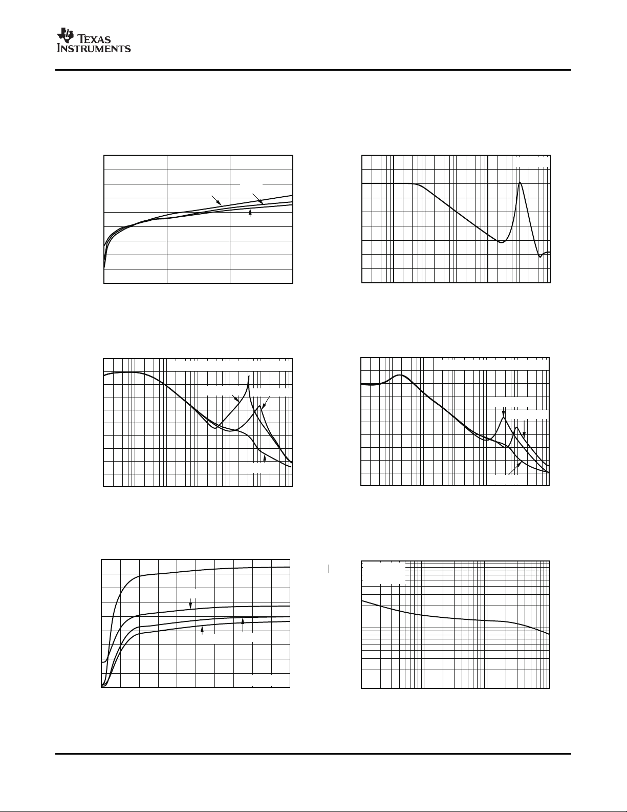
At TJ= +25 ° C, V
unless otherwise noted.
= 1.5V, VIN= V
OUT
V
TYPICAL CHARACTERISTICS (continued)
OUT(TYP)
DROPOUT VOLTAGE vs
BIAS
I
AND TEMPERATURE V
OUT
+ 0.3V, V
BIAS
= 3.3V, I
= 50mA, EN = VIN, CIN= 1 µ F, C
OUT
TPS74301
SBVS065E – DECEMBER 2005 – REVISED MAY 2007
= 4.7 µ F, and C
BIAS
PSRR vs FREQUENCY
BIAS
= 10 µ F,
OUT
Figure 9. Figure 10.
VINPSRR vs FREQUENCY VINPSRR vs FREQUENCY
Figure 11. Figure 12.
VINPSRR vs VIN– V
OUT
NOISE SPECTRAL DENSITY
Figure 13. Figure 14.
Submit Documentation Feedback
7

www.ti.com
20mV/div
20mV/div
20mV/div
20mV/div
1V/div
Time(50 s/div)m
4.3V
C =2x470 F(OSCON)
OUT
m
C =100 F(Cer.)
OUT
m
C =10 F(Cer.)
OUT
m
1V/ sm
3.3V
C =0 F
OUT
m
4.3V
10mV/div
10mV/div
10mV/div
10mV/div
500mV/div
Time(50 s/div)m
C =2x470 F(OSCON)
OUT
m
C =100 F(Cer.)
OUT
m
C =10 F(Cer.)
OUT
m
C =0 F
OUT
m
2.5V
1.5V
V =1.2V
OUT
1V/ sm
50mV/div
50mV/div
50mV/div
50mV/div
1A/div
Time(50 s/div)m
50mA
C =2x470 F(OSCON)
OUT
m
C =100 F(Cer.)
OUT
m
C =10 F(Cer.)
OUT
m
1A/ sm
C =0 F
OUT
m
1.5A
500mV/div
Time(20ms/div)
V
PG
V
TRACK
I =500mA
OUT
V
OUT
1V/div
Time(20ms/div)
V (500mV/div)
PG
V
OUT
V =V
IN BIAS EN
=V
2.85
2.65
2.45
2.25
2.05
1.85
1.65
1.45
1.25
0
0.5 1.0
BiasCurrent(mA)
I (A)
OUT
1.5
+125 C°
+25 C°
- °40 C
TPS74301
SBVS065E – DECEMBER 2005 – REVISED MAY 2007
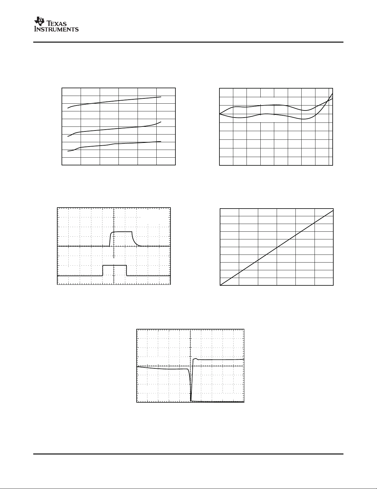
At TJ= +25 ° C, V
unless otherwise noted.
= 1.5V, VIN= V
OUT
V
LINE TRANSIENT VINLINE TRANSIENT (1.5A)
BIAS
Figure 15. Figure 16.
OUTPUT LOAD TRANSIENT RESPONSE TRACKING RESPONSE
TYPICAL CHARACTERISTICS (continued)
OUT(TYP)
+ 0.3V, V
BIAS
= 3.3V, I
= 50mA, EN = VIN, CIN= 1 µ F, C
OUT
= 4.7 µ F, and C
BIAS
= 10 µ F,
OUT
8
Figure 17. Figure 18.
POWER-UP/POWER-DOWN I
Figure 19. Figure 20.
Submit Documentation Feedback
vs I
BIAS
AND TEMPERATURE
OUT
www.ti.com
3.0
2.8
2.6
2.4
2.2
2.0
1.8
1.6
1.4
1.2
1.0
2.0
2.5 3.0 3.5 4.0 4.5
BiasCurrent(mA)
V (V)
BIAS
5.0
+125 C°
+25 C°
- °40 C
0.45
0.40
0.35
0.30
0.25
0.20
0.15
0.10
0.05
0
-40
-20 0 20 40 60 80 100
BiasCurrent( A)m
JunctionTemperature( C)°
120
V =2.375V
BIAS
V =5.5V
BIAS
1V/div
1V/div
Time(50 s/div)m
V
OUT
0V
1.1V
V
EN
V =V
I =1.5A
TRACK IN
OUT
1.0
0.9
0.8
0.7
0.6
0.5
0.4
0.3
0.2
0.1
0
V Low-LevelPGVoltage(V)
OL
0
2 4
6 8 10
12
PGCurrent(mA)
Time(20 s/div)m
V
OUT
50mV/div
I
OUT
500mA/div
OutputOpen
OutputShorted
At TJ= +25 ° C, V
unless otherwise noted.
= 1.5V, VIN= V
OUT
TYPICAL CHARACTERISTICS (continued)
AND V
+ 0.3V, V
OUT
OUT(TYP)
I
vs V
BIAS
BIAS
Figure 21. Figure 22.
BIAS
= 3.3V, I
= 50mA, EN = VIN, CIN= 1 µ F, C
OUT
I
BIAS
TPS74301
SBVS065E – DECEMBER 2005 – REVISED MAY 2007
= 4.7 µ F, and C
BIAS
SHUTDOWN vs TEMPERATURE
= 10 µ F,
OUT
TURN-ON RESPONSE–QFN PACKAGE LOW-LEVEL PG VOLTAGE vs PG CURRENT
Figure 23. Figure 24.
OUTPUT SHORT-CIRCUIT RECOVERY
Submit Documentation Feedback
Figure 25.
9

www.ti.com
R
1
R
5
R
3
R
4
R
2
V
OUT
C
OUT
Optional
PG
OUT
FB
IN
BIAS
TRACK
GND
V
IN
V
BIAS
C
IN
C
BIAS
V
TRACK
V
PG
TPS74301
V =0.8
OUT
´ 1+
R
1
R
2
(
)
EN
TPS74301
SBVS065E – DECEMBER 2005 – REVISED MAY 2007
APPLICATION INFORMATION
The TPS74301 belongs to a family of new Figure 26 is a typical application circuit for the
generation ultra-low dropout regulators that feature TPS74301 adjustable device.
soft-start and tracking capabilities. These regulators
use a low current bias input to power all internal
control circuitry, allowing the NMOS pass transistor
to regulate very low input and output voltages.
The use of an NMOS-pass FET offers several critical specifications, R
advantages for many applications. Unlike a PMOS
topology device, the output capacitor has little effect
on loop stability. This architecture allows the
TPS74301 to be stable with any or even no output
capacitor. Transient response is also superior to
PMOS topologies, particularly for low V
IN
applications.
The TPS74301 features a TRACK pin that allows the
output to track an external supply. This feature is
useful in minimizing the stress on ESD structures
that are present between the CORE and I/O power
pins of many processors. A power-good (PG) output
is also available to allow supply monitoring and
sequencing of follow-on supplies. To control the
output turn-on, an enable (EN) pin with hysteresis
and deglitch is provided to allow slow-ramping
signals to be utilized for sequencing the device. The
low V
and V
IN
OUT
capability allows for inexpensive,
easy-to-design, and efficient linear regulation
between the multiple supply voltages often present in
processor intensive systems.
R
and R
1
can be calculated for any output voltage
2
using the formula shown in Figure 26 . Refer to
Table 1 for sample resistor values of common output
voltages. In order to achieve the maximum accuracy
should be ≤ 4.99k Ω .
2
INPUT, OUTPUT, AND BIAS CAPACITOR REQUIREMENTS
The device does not require any output capacitor for
stability. If an output capacitor is needed, the device
is designed to be stable for all available types and
values of output capacitance. The device is also
stable with multiple capacitors in parallel, of any type
or value.
The capacitance required on the IN and BIAS pins is
strongly dependent on the input supply source
impedance. To counteract any inductance in the
input, the minimum recommended capacitor for V
and V
the same supply, the recommended minimum
capacitor for V
capacitors should be used on the input; ceramic X5R
and X7R capacitors are preferred. These capacitors
should be placed as close the pins as possible for
optimum performance.
BIAS
is 1 µ F. If V
BIAS
and V
IN
are connected to
BIAS
is 4.7 µ F. Good quality, low ESR
IN
10
Figure 26. Typical Application Circuit for the TPS74301 (Adjustable)
Submit Documentation Feedback

www.ti.com
TRANSIENT RESPONSE
Reference
SimplifiedBlock Diagram
V
OUT
OUT
BIAS
FB
IN
V =5V 5%
BIAS
±
V =1.8V
V =1.5V
I =1.5A
Efficiency=83%
IN
OUT
OUT
Reference
SimplifiedBlock Diagram
BIAS
FB
IN
V
IN
V =3.3V 5%
BIAS
±
V =3.3V 5%
V =1.5V
I =1.5A
Efficiency=45%
IN
OUT
OUT
±
V
OUT
OUT
The TPS74301 was designed to have transient
response within 5% for most applications without any
output capacitor. In some cases, the transient
response may be limited by the transient response of
the input supply. This limitation is especially true in
applications where the difference between the input
and output is less than 300mV. In this case, adding
additional input capacitance improves the transient
response much more than just adding additional
output capacitance would do. With a solid input
supply, adding additional output capacitance reduces
undershoot and overshoot during a transient at the
expense of a slightly longer V
recovery time.
OUT
Refer to Figure 17 in the Typical Characteristics
section. Since the TPS74301 is stable without an
output capacitor, many applications may allow for
little or no capacitance at the LDO output. For these
applications, local bypass capacitance for the device
under power may be sufficient to meet the transient
requirements of the application. This design reduces
the total solution cost by avoiding the need to use
expensive high-value capacitors at the LDO output.
DROPOUT VOLTAGE
The TPS74301 offers industry-leading dropout
performance, making it well-suited for high-current
low V
dropout of the TPS74301 allows the device to be
used instead of a DC/DC converter and still achieve
good efficiencies. This efficiency allows users to
rethink the power architecture for their applications to
find the smallest, simplest, and lowest cost solution.
IN
/low V
applications. The extremely low
OUT
TPS74301
SBVS065E – DECEMBER 2005 – REVISED MAY 2007
Figure 27. Typical Application of the TPS74301
Using an Auxiliary Bias Rail
The second specification (see Figure 28 ), referred to
as V
BIAS together. This option allows the device to be
used in applications where an auxiliary bias voltage
is unavailable or low dropout is not required. Dropout
is limited by BIAS in these applications because
V
BIAS
therefore must be 1.4V above V
Dropout, is for users who wish to tie IN and
BIAS
provides the gate drive to the pass FET, and
.
OUT
There are two different specifications for dropout
voltage with the TPS74301. The first specification (as
shown in Figure 27 ) is referred to as V
is for users wishing to apply an external bias voltage
to achieve low dropout. This specification assumes
that V
case for V
tolerance and with V
than 3.3V × 0.95 or V
dropout is less than specified.
is at least 1.62V above V
BIAS
when powered by a 3.3V rail with 5%
BIAS
= 1.5V. If V
OUT
is less than 1.5V, V
OUT
IN
OUT
Dropout and
, which is the
is higher
BIAS
Submit Documentation Feedback
IN
Figure 28. Typical Application of the TPS74301
Without an Auxiliary Bias
11
www.ti.com
V
N
ǒ
mV
RMS
Ǔ
+ 25
ǒ
mV
RMS
V
Ǔ
V
OUT
(V)
IN
BIAS
EN
OUT
PG
SS
TPS74201LDO1
(1)
DSP
IN
I/O
CORE
BIAS
EN
OUT
PG
TRACK
TPS74301LDO2
(1)
R
3
32.4kW
R
4
10kW
R
1
R
2
5V
3.3V
1.2V
NOTES:(1)CapacitorsonIN,BIAS,andOUTalongwiththeresistors
necessarytosettheoutputvoltagehavebeenomittedforsimplification.
(2)LowestvalueforV andhighestvalueforR shouldbeused
inthiscalculation.R mustbethecloseststandardvaluebelowthe
calculatedvalueforproperratiometricsequencing.
CORE 2
1
I/O
T mei
C REO
V
OUT
SIMU TL A E USSEQUENCINGN O
RATIOMETRICSEQUENCING
(2)
C REO
I/O
xR
2
V CCIO- 0.808
R1=
0.808
xR
2
V CC
CORE
- 0.8
R1=
0.8
TPS74301
SBVS065E – DECEMBER 2005 – REVISED MAY 2007
PROGRAMMABLE SEQUENCING WITH SEQUENCING REQUIREMENTS
TRACK
The TPS74301 features a track pin that allows the sequenced in any order without causing damage to
output to track an external supply at start-up. While the device. However, for the track function to work as
the TRACK input is below 0.8V, the error amplifier intended, certain sequencing rules must be applied.
regulates the FB pin to the TRACK input. Properly V
choosing the resistor divider network (R
shown in Figure 29 enables the regulator output to faster than the external supply being tracked so that
track the external supply to obtain a simultaneous or the tracking signal will not drive the device into V
ratiometric start-up. Once the TRACK input reaches dropout as V
0.8V, the error amplifier regulates the FB pin to the sequence the tracking device is to have V
0.8V internal reference. Further increases to the and V
TRACK input have no effect. before enabling the master supply to initiate the
and R2) as the track signal starts to ramp. V
1
The device can have V
must be present and the device enabled before
BIAS
ramps up. The preferred method to
OUT
above the minimum required voltages
EN
, V
IN
BIAS
, V
, and V
EN
should ramp up
IN
, V
IN
startup sequence. This method is illustrated in
Figure 29 . Resistors R
and R
3
4
disable the master
supply until the input voltage is above 3.52V
(typical).
If the TRACK pin is not needed it should be
connected to VIN. Configured in this way, the device
starts up typically within 40 µ s, which may result in
large inrush current that could cause the input supply
to droop. If soft-start is needed, consider the
TPS74201 or TPS74401 devices.
TRACK
IN
,
BIAS
OUTPUT NOISE
The TPS74301 provides low output noise when a
soft-start capacitor is used. When the device reaches
the end of the soft-start cycle, the soft-start capacitor
serves as a filter for the internal reference. By using
a 0.001 µ F soft-start capacitor, the output noise is
reduced by half and is typically 30 µ V
output (10Hz to 100kHz). Because most of the
output noise is generated by the internal reference,
the noise is a function of the set output voltage. The
RMS noise with a 0.001 µ F soft-start capacitor is
given in Equation 1 .
The low output noise of the TPS74301 makes it a
good choice for powering transceivers, PLLs, or
other noise-sensitive circuitry.
for a 1.2V
RMS
(1)
ENABLE/SHUTDOWN
Figure 29. Various Sequencing Methods Using
the TRACK Pin
The maximum recommended value for R
Once R
the equations given in Figure 29 .
is selected, R
2
1
is 100k Ω .
2
is calculated using one of
The enable (EN) pin is active high and is compatible
with standard digital signaling levels. V
turns the regulator off, while V
EN
above 1.1V turns
below 0.4V
EN
the regulator on. Unlike many regulators, the enable
circuitry has hysteresis and deglitching for use with
relatively slow-ramping analog signals. This
configuration allows the TPS74301 to be enabled by
connecting the output of another supply to the EN
pin. The enable circuitry typically has 50mV of
hysteresis and a deglitch circuit to help avoid on-off
cycling because of small glitches in the V
signal.
EN
12
Submit Documentation Feedback

www.ti.com
P
D
+
ǒ
VIN* V
OUT
Ǔ
I
OUT
TPS74301
SBVS065E – DECEMBER 2005 – REVISED MAY 2007
The enable threshold is typically 0.8V and varies with dissipation, thermal resistance, and ambient
temperature and process variations. Temperature temperature the thermal protection circuit may cycle
variation is approximately –1mV/ ° C; therefore, on and off. This cycling limits the dissipation of the
process variation accounts for most of the variation regulator, protecting it from damage as a result of
in the enable threshold. If precise turn-on timing is overheating.
required, a fast rise-time signal should be used to
enable the TPS74301.
If not used, EN can be connected to either IN or heatsinking. For reliable operation, junction
BIAS. If EN is connected to IN, it should be temperature should be limited to +125 ° C maximum.
connected as close as possible to the largest To estimate the margin of safety in a complete
capacitance on the input to prevent voltage droops design (including heatsink), increase the ambient
on that line from triggering the enable circuit. temperature until thermal protection is triggered; use
POWER-GOOD (QFN Package Only)
The power-good (PG) pin is an open-drain output
and can be connected to any 5.5V or lower rail
through an external pull-up resistor. This pin requires
at least 1.1V on V
The PG output is high-impedance when V
greater than V
V
drops below 1.9V, the open-drain output turns
BIAS
IT
in order to have a valid output.
BIAS
+ V
. If V
HYS
drops below V
OUT
is
OUT
or if
IT
on and pulls the PG output low. The PG pin also
asserts when the device is disabled. The
recommended operating condition of PG pin sink
current is up to 1mA, so the pull-up resistor for PG
should be in the range of 10k Ω to 1M Ω . PG is only
provided on the QFN package. If output voltage DISSIPATION
monitoring is not needed, the PG pin can be left
floating.
INTERNAL CURRENT LIMIT
The TPS74301 features a factory-trimmed, accurate
current limit that is flat over temperature and supply
voltage. The current limit allows the device to supply
surges of up to 1.8A and maintain regulation. The
current limit responds in about 10 µ s to reduce the
current during a short-circuit fault. Recovery from a
short-circuit condition is well-controlled and results in
very little output overshoot when the load is
removed. See Figure 25 in the Typical
Characteristics section for output short-circuit
recovery performance.
The internal current limit protection circuitry of the
TPS74301 is designed to protect against overload
conditions. It is not intended to allow operation above
the rated current of the device. Continuously running
the TPS74301 above the rated current degrades
device reliability.
THERMAL PROTECTION
Thermal protection disables the output when the
junction temperature rises to approximately +155 ° C,
allowing the device to cool. When the junction
temperature cools to approximately +140 ° C, the
output circuitry is enabled. Depending on power
Activation of the thermal protection circuit indicates
excessive power dissipation or inadequate
worst-case loads and signal conditions. For good
reliability, thermal protection should trigger at least
+30 ° C above the maximum expected ambient
condition of the application. This condition produces
a worst-case junction temperature of +125 ° C at the
highest expected ambient temperature and
worst-case load.
The internal protection circuitry of the TPS74301 is
designed to protect against overload conditions. It is
not intended to replace proper heatsinking.
Continuously running the TPS74301 into thermal
shutdown degrades device reliability.
LAYOUT RECOMMENDATIONS AND POWER
An optimal layout can greatly improve transient
performance, PSRR, and noise. To minimize the
voltage droop on the input of the device during load
transients, the capacitance on IN and BIAS should
be connected as close as possible to the device.
This capacitance also minimizes the effects of
parasitic inductance and resistance of the input
source and can therefore improve stability. To
achieve optimal transient performance and accuracy,
the top side of R
as close as possible to the load. If BIAS is connected
to IN, it is recommended to connect BIAS as close to
the sense point of the input supply as possible. This
connection minimizes the voltage droop on BIAS
during transient conditions and can improve the
turn-on response.
Knowing the device power dissipation and proper
sizing of the thermal plane that is connected to the
tab or pad is critical to avoiding thermal shutdown
and ensuring reliable operation. Power dissipation of
the device depends on input voltage and load
conditions, and can be calculated using Equation 2 :
in Figure 26 should be connected
1
(2)
Submit Documentation Feedback
13

www.ti.com
R
qJA
+
(
)125
O
C * T
A
)
P
D
55
50
45
40
35
30
25
0
0.5 1.0 1.5 2.0 2.5 3.0 3.5 4.0
q
JA
(
°C/W)
Area(in )
2
4.5
0LFM
150LFM
250LFM
T
J
R
qJC
R
qCS
R
qSA
T
C
T
S
T
A
4-layer.0.062” FR4
Viasare0.012” diameter,plated
Top/Bottomlayersare2oz.copper
Innerlayersare1oz.copper
0.062in.
R
qJA
= R +R +R
q q qJC CS SA
PCBCrossSection
PCBTopView
0.5in
2
1.0in
2
2.0in
2
TPS74301
SBVS065E – DECEMBER 2005 – REVISED MAY 2007
Power dissipation can be minimized and greater maximum junction-to-ambient thermal resistance
efficiency can be achieved by using the lowest depends on the maximum ambient temperature,
possible input voltage necessary to achieve the maximum device junction temperature, and power
required output voltage regulation. dissipation of the device, and can be calculated
On both the QFN (RGW) and DDPAK (KTW)
packages, the primary conduction path for heat is
through the exposed pad or tab to the printed circuit
board (PCB). The pad or tab can be connected to
ground or be left floating; however, it should be
attached to an appropriate amount of copper PCB
area to ensure the device does not overheat. The
using Equation 3 :
Knowing the maximum R
and system air flow, the
θ JA
minimum amount of PCB copper area needed for
appropriate heatsinking can be calculated using
Figure 30 through Figure 34 .
(3)
Figure 30. PCB Layout and Corresponding R
14
Data, Buried Thermal Plane, No Vias Under Thermal Pad
θ JA
Submit Documentation Feedback

www.ti.com
T
J
R
qJC
R
qCS
R
qSA
T
C
T
S
T
A
4-layer.0.062” FR4
Viasare0.012” diameter,plated
Top/Bottomlayersare2oz.copper
Innerlayersare1oz.copper
0.062in.
R
qJA
= R +R +R
q q qJC CS SA
50
45
40
35
30
25
20
0
0.5 1.0 1.5 2.0 2.5 3.0 3.5
q
JA
(°C/W)
Area(in )
2
4.0
0LFM
150LFM
250LFM
PCBCrossSection
PCBTopView
0.5in
2
1.0in
2
2.0in
2
TPS74301
SBVS065E – DECEMBER 2005 – REVISED MAY 2007
Figure 31. PCB Layout and Corresponding R
Submit Documentation Feedback
Data, Buried Thermal Plane, Vias Under Thermal Pad
θ JA
15

www.ti.com
4-layer.0.062” FR4
Viasare0.012” diameter,plated
Top/Bottomlayersare2oz.copper
Innerlayersare1oz.copper
T
J
R
qJC
R
qCS
R
qSA
T
C
T
S
T
A
0.062in.
R
qJA
= R +R +R
q q qJC CS SA
90
80
70
60
50
40
30
0
0.5 1.0 1.5 2.0 2.5 3.0 3.5
q
JA
(°C/W)
Area(in )
2
4.0
0LFM
150LFM
250LFM
PCBCrossSection
PCBTopView
0.5in
2
1.0in
2
2.0in
2
TPS74301
SBVS065E – DECEMBER 2005 – REVISED MAY 2007
Figure 32. PCB Layout and Corresponding R
Data, Top Layer Thermal Plane
θ JA
16
Submit Documentation Feedback

www.ti.com
35
30
25
20
15
0
0.5 1.0 1.5 2.0 2.5 3.0 3.5
q
JA
(°C/W)
Area(in )
2
4.0
0LFM
T
J
R
qJC
R
qCS
R
qSA
T
C
T
S
T
A
4-layer.0.062” FR4
Viasare0.012” diameter,plated
Top/Bottomlayersare2oz.copper
Innerlayersare1oz.copper
0.062in.
R
qJA
= R +R +R
q q qJC CS SA
PCBCrossSection
PCBTopView
0.5in
2
1.0in
2
2.0in
2
TPS74301
SBVS065E – DECEMBER 2005 – REVISED MAY 2007
Figure 33. PCB Layout and Corresponding R
Submit Documentation Feedback
θ JA
, Buried Thermal Plane
17

www.ti.com
4-layer.0.062” FR4
Viasare0.012” diameter,plated
Top/Bottomlayersare2oz.copper
Innerlayersare1oz.copper
T
J
R
qJC
R
qCS
R
qSA
T
C
T
S
T
A
0.062in.
R
qJA
= R +R +R
q q qJC CS SA
55
50
45
40
35
30
25
20
15
10
0
0.5 1.0 1.5 2.0 2.5 3.0 3.5 4.0
q
JA
(°C/W)
Area(in )
2
4.5
0LFM
PCBCrossSection
PCBTopView
0.5in
2
1.0in
2
2.0in
2
TPS74301
SBVS065E – DECEMBER 2005 – REVISED MAY 2007
Figure 34. PCB Layout and Corresponding R
18
Submit Documentation Feedback
, Top Layer Thermal Plane
θ JA

PACKAGE OPTION ADDENDUM
www.ti.com
5-Feb-2007
PACKAGING INFORMATION
Orderable Device Status
(1)
Package
Type
Package
Drawing
Pins Package
Qty
Eco Plan
TPS74301KTWR ACTIVE DDPAK KTW 7 500 Green (RoHS &
no Sb/Br)
TPS74301KTWRG3 ACTIVE DDPAK KTW 7 500 Green (RoHS &
no Sb/Br)
TPS74301KTWT ACTIVE DDPAK KTW 7 50 Green (RoHS &
no Sb/Br)
TPS74301KTWTG3 ACTIVE DDPAK KTW 7 50 Green (RoHS &
no Sb/Br)
TPS74301RGWR ACTIVE QFN RGW 20 3000 Green (RoHS &
no Sb/Br)
TPS74301RGWRG4 ACTIVE QFN RGW 20 3000 Green (RoHS &
no Sb/Br)
TPS74301RGWT ACTIVE QFN RGW 20 250 Green (RoHS &
no Sb/Br)
TPS74301RGWTG4 ACTIVE QFN RGW 20 250 Green (RoHS &
no Sb/Br)
(1)
The marketing status values are defined as follows:
ACTIVE: Product device recommended for new designs.
LIFEBUY: TI has announced that the device will be discontinued, and a lifetime-buy period is in effect.
NRND: Not recommended for new designs. Device is in production to support existing customers, but TI does not recommend using this part in
a new design.
PREVIEW: Device has been announced but is not in production. Samples may or may not be available.
OBSOLETE: TI has discontinued the production of the device.
(2)
Lead/Ball Finish MSL Peak Temp
CU SN Level-3-245C-168 HR
CU SN Level-3-245C-168 HR
CU SN Level-3-245C-168 HR
CU SN Level-3-245C-168 HR
CU NIPDAU Level-2-260C-1 YEAR
CU NIPDAU Level-2-260C-1 YEAR
CU NIPDAU Level-2-260C-1 YEAR
CU NIPDAU Level-2-260C-1 YEAR
(3)
(2)
Eco Plan - The planned eco-friendly classification: Pb-Free (RoHS), Pb-Free (RoHS Exempt), or Green (RoHS & no Sb/Br) - please check
http://www.ti.com/productcontent for the latest availability information and additional product content details.
TBD: The Pb-Free/Green conversion plan has not been defined.
Pb-Free (RoHS): TI's terms "Lead-Free" or "Pb-Free" mean semiconductor products that are compatible with the current RoHS requirements
for all 6 substances, including the requirement that lead not exceed 0.1% by weight in homogeneous materials. Where designed to be soldered
at high temperatures, TI Pb-Free products are suitable for use in specified lead-free processes.
Pb-Free (RoHS Exempt): This component has a RoHS exemption for either 1) lead-based flip-chip solder bumps used between the die and
package, or 2) lead-based die adhesive used between the die and leadframe. The component is otherwise considered Pb-Free (RoHS
compatible) as defined above.
Green (RoHS & no Sb/Br): TI defines "Green" to mean Pb-Free (RoHS compatible), and free of Bromine (Br) and Antimony (Sb) based flame
retardants (Br or Sb do not exceed 0.1% by weight in homogeneous material)
(3)
MSL, Peak Temp. -- The Moisture Sensitivity Level rating according to the JEDEC industry standard classifications, and peak solder
temperature.
Important Information and Disclaimer:The information provided on this page represents TI's knowledge and belief as of the date that it is
provided. TI bases its knowledge and belief on information provided by third parties, and makes no representation or warranty as to the
accuracy of such information. Efforts are underway to better integrate information from third parties. TI has taken and continues to take
reasonable steps to provide representative and accurate information but may not have conducted destructive testing or chemical analysis on
incoming materials and chemicals. TI and TI suppliers consider certain information to be proprietary, and thus CAS numbers and other limited
information may not be available for release.
In no event shall TI's liability arising out of such information exceed the total purchase price of the TI part(s) at issue in this document sold by TI
to Customer on an annual basis.
Addendum-Page 1

PACKAGE MATERIALS INFORMATION
www.ti.com
17-May-2007
TAPE AND REEL INFORMATION
Pack Materials-Page 1

PACKAGE MATERIALS INFORMATION
www.ti.com
Device Package Pins Site Reel
Diameter
(mm)
TPS74301RGWR RGW 20 MLA 330 12 5.3 5.3 1.5 8 12 PKGORN
TPS74301RGWT RGW 20 MLA 180 12 5.3 5.3 1.5 8 12 PKGORN
Reel
Width
(mm)
A0 (mm) B0 (mm) K0 (mm) P1
(mm)W(mm)
17-May-2007
Pin1
Quadrant
T2TR-MS
P
T2TR-MS
P
TAPE AND REEL BOX INFORMATION
Device Package Pins Site Length (mm) Width (mm) Height (mm)
TPS74301RGWR RGW 20 MLA 346.0 346.0 29.0
TPS74301RGWT RGW 20 MLA 190.0 212.7 31.75
Pack Materials-Page 2

PACKAGE MATERIALS INFORMATION
www.ti.com
17-May-2007
Pack Materials-Page 3


MECHANICAL DATA
MPSF015 – AUGUST 2001
KTW (R-PSFM-G7) PLASTIC FLANGE-MOUNT
0.0625 (1,587)
0.0585 (1,485)
H
0.605 (15,37)
0.595 (15,11)
H
0.370 (9,40)
0.330 (8,38)
C
C
0.410 (10,41)
0.385 (9,78)
0.303 (7,70)
0.297 (7,54)
0.050 (1,27)
0.034 (0,86)
F
0.022 (0,57)
0.010 (0,25)
–A–
0.055 (1,40)
0.045 (1,14)
A
0.012 (0,305)
0.000 (0,00)
0.019 (0,48)
0.017 (0,43)
0.026 (0,66)
C
0.014 (0,36)
B
A
M
M
C
M
0.006
–B–
0.104 (2,64)
0.096 (2,44)
0.064 (1,63)
0.056 (1,42)
0.187 (4,75)
0.179 (4,55)
H
0°~3°
0.304 (7,72)
0.296 (7,52)
0.300 (7,62)
0.252 (6,40)
0.183 (4,65)
0.170 (4,32)
NOTES: A. All linear dimensions are in inches (millimeters).
B. This drawing is subject to change without notice.
C. Lead width and height dimensions apply to the
plated lead.
D. Leads are not allowed above the Datum B.
E. Stand–off height is measured from lead tip
with reference to Datum B.
F. Lead width dimension does not include dambar
protrusion. Allowable dambar protrusion shall not
cause the lead width to exceed the maximum
dimension by more than 0.003”.
G. Cross–hatch indicates exposed metal surface.
H. Falls within JEDEC MO–169 with the exception
of the dimensions indicated.
4201284/A 08/01
POST OFFICE BOX 655303 • DALLAS, TEXAS 75265

IMPORTANT NOTICE
Texas Instruments Incorporated and its subsidiaries (TI) reserve the right to make corrections, modifications, enhancements,
improvements, and other changes to its products and services at any time and to discontinue any product or service without notice.
Customers should obtain the latest relevant information before placing orders and should verify that such information is current and
complete. All products are sold subject to TI’s terms and conditions of sale supplied at the time of order acknowledgment.
TI warrants performance of its hardware products to the specifications applicable at the time of sale in accordance with TI’s
standard warranty. Testing and other quality control techniques are used to the extent TI deems necessary to support this
warranty. Except where mandated by government requirements, testing of all parameters of each product is not necessarily
performed.
TI assumes no liability for applications assistance or customer product design. Customers are responsible for their products and
applications using TI components. To minimize the risks associated with customer products and applications, customers should
provide adequate design and operating safeguards.
TI does not warrant or represent that any license, either express or implied, is granted under any TI patent right, copyright, mask
work right, or other TI intellectual property right relating to any combination, machine, or process in which TI products or services
are used. Information published by TI regarding third-party products or services does not constitute a license from TI to use such
products or services or a warranty or endorsement thereof. Use of such information may require a license from a third party under
the patents or other intellectual property of the third party, or a license from TI under the patents or other intellectual property of TI.
Reproduction of information in TI data books or data sheets is permissible only if reproduction is without alteration and is
accompanied by all associated warranties, conditions, limitations, and notices. Reproduction of this information with alteration is an
unfair and deceptive business practice. TI is not responsible or liable for such altered documentation.
Resale of TI products or services with statements different from or beyond the parameters stated by TI for that product or service
voids all express and any implied warranties for the associated TI product or service and is an unfair and deceptive business
practice. TI is not responsible or liable for any such statements.
TI products are not authorized for use in safety-critical applications (such as life support) where a failure of the TI product would
reasonably be expected to cause severe personal injury or death, unless officers of the parties have executed an agreement
specifically governing such use. Buyers represent that they have all necessary expertise in the safety and regulatory ramifications
of their applications, and acknowledge and agree that they are solely responsible for all legal, regulatory and safety-related
requirements concerning their products and any use of TI products in such safety-critical applications, notwithstanding any
applications-related information or support that may be provided by TI. Further, Buyers must fully indemnify TI and its
representatives against any damages arising out of the use of TI products in such safety-critical applications.
TI products are neither designed nor intended for use in military/aerospace applications or environments unless the TI products are
specifically designated by TI as military-grade or "enhanced plastic." Only products designated by TI as military-grade meet military
specifications. Buyers acknowledge and agree that any such use of TI products which TI has not designated as military-grade is
solely at the Buyer's risk, and that they are solely responsible for compliance with all legal and regulatory requirements in
connection with such use.
TI products are neither designed nor intended for use in automotive applications or environments unless the specific TI products
are designated by TI as compliant with ISO/TS 16949 requirements. Buyers acknowledge and agree that, if they use any
non-designated products in automotive applications, TI will not be responsible for any failure to meet such requirements.
Following are URLs where you can obtain information on other Texas Instruments products and application solutions:
Products Applications
Amplifiers amplifier.ti.com Audio www.ti.com/audio
Data Converters dataconverter.ti.com Automotive www.ti.com/automotive
DSP dsp.ti.com Broadband www.ti.com/broadband
Interface interface.ti.com Digital Control www.ti.com/digitalcontrol
Logic logic.ti.com Military www.ti.com/military
Power Mgmt power.ti.com Optical Networking www.ti.com/opticalnetwork
Microcontrollers microcontroller.ti.com Security www.ti.com/security
RFID www.ti-rfid.com Telephony www.ti.com/telephony
Low Power www.ti.com/lpw Video & Imaging www.ti.com/video
Wireless
Wireless www.ti.com/wireless
Mailing Address: Texas Instruments, Post Office Box 655303, Dallas, Texas 75265
Copyright © 2007, Texas Instruments Incorporated
 Loading...