

TPS718xx
TPS719xx
GND
EN1
EN2
OUT2
IN OUT1
V
IN
V
OUT
V
OUT
1 Fm
1 Fm
1 Fm
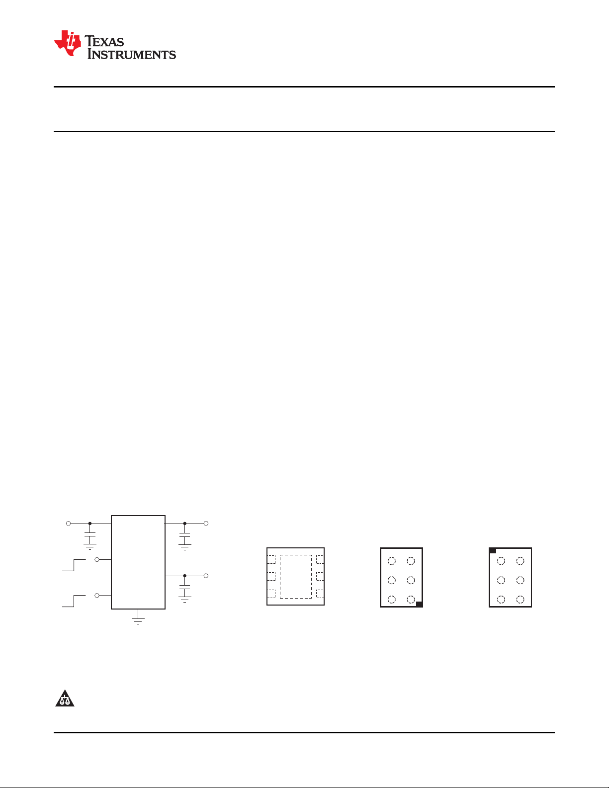
TypicalApplicationCircuit
2.7Vto6.5V 0.9Vto3.6V
0.9V 3.6V-
On
Off
On
Off
EN1
GND
GND
EN2
6
5
4
OUT1
IN
OUT2
1
2
3
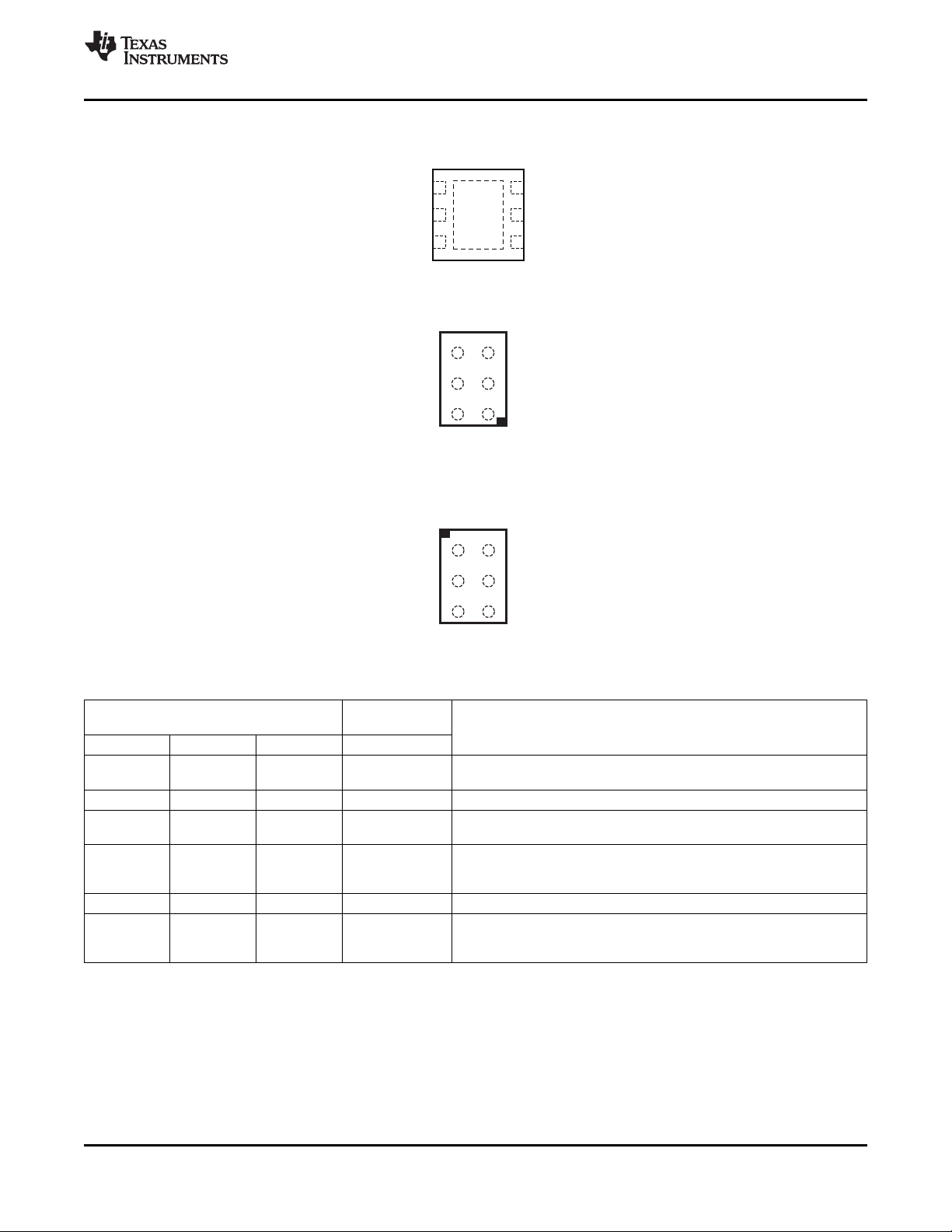
TPS718xx,TPS719xx
DRVPackage
2mmx2mmSON-6
(TopView)
OUT1
IN
OUT2
EN1
GND
EN2
A1
B1
C1
A2
B2
C2
TPS718Axx,TPS719Axx
YZCPackage
6-BALLWCSP
(TopView)
OUT1
IN
OUT2
EN1
GND
EN2
C2
B2
A2
C1
B1
A1
TPS718xx,TPS719xx
YZCPackage
6-BALLWCSP
(TopView)
TPS718xx
TPS719xx
www.ti.com
..................................................................................................................................................... SBVS088C – FEBRUARY 2007 – REVISED MAY 2008
Dual, 200mA Output, Low Noise, High PSRR
Low-Dropout Linear Regulators
1
FEATURES DESCRIPTION
23
• Dual, 200mA High-Performance LDOs
• Low Total Quiescent Current: 90 µ A with Both
LDOs Enabled
• Low Noise: 70 µ V
• Active Output Pulldown (TPS719xx)
• Independent Enables for Each LDO
• PSRR: 65dB at 1kHz, 45dB at 1MHz
• Available in Multiple Fixed-Output Voltage
Combinations from 0.9V to 3.6V Using
Innovative Factory EEPROM Programming
• Fast Start-Up Time: 160 µ s
• Over-Current, Over-Temperature and
Under-Voltage Protection
• Low Dropout: 230mV at 200mA
• Stable with 1 µ F Ceramic Output Capacitor
• Available in 2mm × 2mm SON-6 and 6-Ball
WCSP Packages
/V
RMS
The TPS718xx and TPS719xx families of low-dropout
(LDO) regulators offer a high power-supply rejection
ratio (PSRR), low noise, fast start-up, and excellent
line and load transient responses while consuming a
very low 90 µ A (typical) at no load ground current with
both LDOs enabled. The TPS719xx also provides an
active pulldown circuit to quickly discharge output
loads. The TPS718xx and TPS719xx are stable with
ceramic capacitors and use an advanced BiCMOS
fabrication process to yield a typical dropout voltage
of 230mV at 200mA output loads. The TPS718xx and
TPS719xx also use a precision voltage reference and
feedback loop to achieve 3% overall accuracy over all
load, line, process, and temperature variations. Both
families of devices are fully specified from TJ= – 40 ° C
to +125 ° C and are offered in 2mm × 2mm SON-6 and
6-ball Wafer Chip-Scale (WCSP) packages that are
ideal for applications such as mobile handsets and
WLAN that require good thermal dissipation while
maintaining a very small footprint.
APPLICATIONS
• Digital Cameras and Camera Modules
• Cellular Camera and TV Phones
• Wireless LAN, Bluetooth
• Handheld Products
1
Please be aware that an important notice concerning availability, standard warranty, and use in critical applications of
Texas Instruments semiconductor products and disclaimers thereto appears at the end of this data sheet.
2 Bluetooth is a registered trademark of Bluetooth SIG, Inc.
3 All other trademarks are the property of their respective owners.
PRODUCTION DATA information is current as of publication date.
Products conform to specifications per the terms of the Texas
Instruments standard warranty. Production processing does not
necessarily include testing of all parameters.
®
Copyright © 2007 – 2008, Texas Instruments Incorporated
TPS718xx
TPS719xx
SBVS088C – FEBRUARY 2007 – REVISED MAY 2008 .....................................................................................................................................................
www.ti.com
This integrated circuit can be damaged by ESD. Texas Instruments recommends that all integrated circuits be handled with
appropriate precautions. Failure to observe proper handling and installation procedures can cause damage.
ESD damage can range from subtle performance degradation to complete device failure. Precision integrated circuits may be more
susceptible to damage because very small parametric changes could cause the device not to meet its published specifications.
ORDERING INFORMATION
PRODUCT V
(1)
(2) (3)
OUT
TPS718 xx-yywwwz A denotes device with rotated pin 1 orientation of wafer-chipscale package.
TPS718A xx-yywwwz XX is nominal output voltage for LDO1 (for example, 28 = 2.8V).
TPS719 xx-yywwwz YY is nominal output voltage for LDO2.
TPS719A xx-yywwwz WWW is package designator.
Z is tape and reel quantity (R = 3000, T = 250).
Examples: TPS71918 – 285DRVR XX = 18 = 1.8V, YYY = 285 = 2.85V
TPS719185-33DRVR XXX = 185 = 1.85V, YY = 33 = 3.3V
DRV = 2mm x 2mm SON package
Z = R = 3000 piece reel
(1) For the most current package and ordering information see the Package Option Addendum at the end of this document, or see the TI
website at www.ti.com .
(2) Both outputs are programmable from 0.9V to 3.6V in 50mV increments.
(3) Output voltages from 0.9V to 3.6V in 50mV increments are available through the use of innovative factory EEPROM programming;
minimum order quantities may apply. Contact factory for details and availability.
ABSOLUTE MAXIMUM RATINGS
(1)
Over operating temperature range (unless otherwise noted). All voltages are with respect to GND.
PARAMETER TPS718xx, TPS719xx UNIT
Input voltage range, V
Enable voltage range, V
Output voltage range, V
IN
and V
EN1
OUT
EN2
Peak output current Internally limited
Output short-circuit duration Indefinite
Junction temperature range, T
Storage temperature range , T
Total continuous power dissipation, P
J
STG
DISS
ESD rating, HBM 2 kV
ESD rating, CDM 500 V
(1) Stresses above these ratings may cause permanent damage. Exposure to absolute maximum conditions for extended periods may
degrade device reliability. These are stress ratings only, and functional operation of the device at these or any other conditions beyond
those specified is not implied.
– 0.3 to +7.0 V
– 0.3 to VIN+ 0.3V V
– 0.3 to +7.0 V
– 55 to +150 ° C
– 55 to +150 ° C
See Dissipation Ratings Table
DISSIPATION RATINGS
BOARD PACKAGE R
(1)
High-K
(1)
High-K
DRV 20 ° C/W 95 ° C/W 10.53mW/ ° C 1053mW 579mW 421mW
YZC 27 ° C/W 190 ° C/W 5.3mW/ ° C 530mW 295mW 215mW
θ JC
R
θ JA
(1) The JEDEC high-K (2s2p) board used to derive this data was a 3in × 3in, multilayer board with 1-ounce internal power and ground
planes and 2-ounce copper traces on top and bottom of the board.
2 Submit Documentation Feedback Copyright © 2007 – 2008, Texas Instruments Incorporated
Product Folder Link(s): TPS718xx TPS719xx
DERATING FACTOR
ABOVE TA= +25 ° C TA< +25 ° C TA= +70 ° C TA= +85 ° C
TPS718xx
TPS719xx
www.ti.com
..................................................................................................................................................... SBVS088C – FEBRUARY 2007 – REVISED MAY 2008
ELECTRICAL CHARACTERISTICS
Over operating temperature range (T
I
= 0.5mA, V
OUT
V
IN
V
, V
OUT1
OUT2
V
, V
OUT1
OUT2
Δ V
/ Δ V
OUT
IN
Δ V
/ Δ I
OUT
OUT
V
DO
I
CL
I
GND
I
SHDN
PSRR VIN= 3.8V, V
V
N
T
STR
T
SHUT
V
EN(HI)
V
EN(LO)
I
EN
UVLO
T
SD
T
J
(1) Minimum VIN= V
(2) V
(3) Time from V
is not measured for devices with V
DO
(4) Time from V
(5) See Shutdown section in the Applications Information for more details.
= V
EN1
= VIN, C
EN2
PARAMETER TEST CONDITIONS MIN TYP MAX UNIT
Input voltage range
Output voltage range 0.9 3.6 V
Output accuracy
Line regulation 130 µ V/V
Load regulation 0mA ≤ I
Dropout voltage
(V
= V
IN
(2)
OUT(NOM)
Output current limit (per output) V
Ground pin current
Shutdown current (I
Power-supply rejection ratio
I
OUT
OUT
= 200mA
Output noise voltage
BW = 100Hz to 100kHz
Startup time
Shutdown time
(3)
(4),(5)
(TPS719xx only) V
Enable high (enabled)
(EN1 and EN2)
Enable low (shutdown)
(EN1 and EN2)
Enable pin current, enabled
(EN1 and EN2)
Undervoltage lockout VINrising 2.38 2.45 2.52 V
Hysteresis VINfalling 150 mV
Thermal shutdown temperature
Operating junction temperature – 40 +125 ° C
+ V
or 2.7V, whichever is greater.
DO
OUT
OUT
= 1.25V to V
EN
= 0.4V to V
EN
OUT
= – 40 ° C to +125 ° C), V
J
= 1.0 µ F, unless otherwise noted. Typical values are at TJ= +25 ° C.
OUT
(1)
Nominal TJ= +25 ° C ± 2.5 mV
Over VIN, I
Temp 0mA ≤ I
, V
OUT
V
I
OUT
I
– 0.1V)
OUT
I
OUT1
I
OUT1
V
)
GND
TJ= – 40 ° C to +85 ° C
V
TJ= – 40 ° C to +85 ° C
f = 100Hz 63 dB
f = 1kHz 63 dB
= 2.8V, f = 10kHz 72 dB
f = 100kHz 58 dB
f = 1MHz 44 dB
RL= 14 Ω , V
C
RL= ∞ , C
VIN≤ 5.5V 1.2 6.5 V
5.5V < VIN≤ 6.5V 1.25 6.5 V
EN1 = EN2 = 6.5V 0.04 1.0 µ A
Shutdown, temperature increasing +160 ° C
Reset, temperature decreasing +140 ° C
= 95% (V
= 5% (V
OUT(NOM)
OUT(NOM)
< 2.8V because minimum VIN= 2.7V.
OUT(NOM)
).
).
= V
IN
OUT(TYP)
+ 0.5V or 2.7V, whichever is greater;
2.7 6.5 V
+ 0.5V ≤ VIN≤ 6.5V
OUT
OUT(NOM)
≤ 200mA
OUT
+ 0.5V ≤ VIN≤ 6.5V,
= 5mA
≤ 200mA 75 µ V/mA
OUT
– 3.0 +3.0 %
= 200mA 230 400 mV
= 0.9 × V
OUT
= I
OUT2
= I
OUT2
≤ 0.4V, 2.7V ≤ VIN< 4.5V,
EN1,2
≤ 0.4V, 4.5V ≤ VIN≤ 6.5V,
EN1,2
= 1.0 µ F
OUT
= 2.8V
OUT
OUT(NOM)
= 0.1mA 90 160 µ A
= 200mA 250 µ A
= 2.8V,
OUT
= 1.0 µ F,
OUT
240 340 575 mA
0.3 3.0 µ A
1.8 µ A
70 × V
OUT
160 µ s
180 µ s
0 0.4 V
µ V
RMS
Copyright © 2007 – 2008, Texas Instruments Incorporated Submit Documentation Feedback 3
Product Folder Link(s): TPS718xx TPS719xx
GND
Bandgap
Bandgap
2.5 Am
2.5 Am
Current
Limit
Thermal
Shutdown
UVLO
Current
Limit
Thermal
Shutdown
UVLO
Enableand
Power
Control
Logic
60W
60W
OUT1
OUT2
EN1
EN2
IN
TPS719only
TPS719only
TPS718xx
TPS719xx
SBVS088C – FEBRUARY 2007 – REVISED MAY 2008 .....................................................................................................................................................
www.ti.com
DEVICE INFORMATION
Figure 1. Functional Block Diagram
4 Submit Documentation Feedback Copyright © 2007 – 2008, Texas Instruments Incorporated
Product Folder Link(s): TPS718xx TPS719xx
EN1
GND
GND
EN2
6
5
4
OUT1
IN
OUT2
1
2
3
OUT1
IN
OUT2
EN1
GND
EN2
C2
B2
A2
C1
B1
A1
TPS718xx
TPS719xx
TPS718Axx
TPS719Axx
OUT1
IN
OUT2
EN1
GND
EN2
A1
B1
C1
A2
B2
C2
TPS718xx
TPS719xx
www.ti.com
..................................................................................................................................................... SBVS088C – FEBRUARY 2007 – REVISED MAY 2008
DRV PACKAGE
SON-6
(TOP VIEW)
YZC PACKAGE
6-BALL WCSP
(TOP VIEW)
YZC PACKAGE
6-BALL WCSP
(TOP VIEW)
PIN DESCRIPTIONS
TPS718xx TPS718Axx
TPS719xx TPS719Axx
NAME DRV YZC YZC DESCRIPTION
OUT1 1 C1 A2
IN 2 B1 B2 Input supply to both regulators.
OUT2 3 A1 C2
EN2 4 A2 C1 Regulator 2. Driving this pin low puts Regulator 2 into shutdown mode,
GND 5 B2 B1 Ground. DRV thermal pad should also be connected to ground.
EN1 6 C2 A1 Regulator 1. Driving this pin low puts Regulator 1 into shutdown mode,
(1) A option denotes devices with rotated Pin 1 orientation on Wafer Chipscale packages.
Copyright © 2007 – 2008, Texas Instruments Incorporated Submit Documentation Feedback 5
Product Folder Link(s): TPS718xx TPS719xx
(1)
(1)
Output of Regulator 1. A small ceramic capacitor (typically ≥ 1 µ F) is
needed from this pin to ground to assure stability.
Output of Regulator 2. A small ceramic capacitor (typically ≥ 1 µ F) is
needed from this pin to ground to assure stability.
Enable pin for Regulator 2. Driving the Enable pin (EN2) high turns on
reducing operating current.
Enable pin for Regulator 1. Driving the Enable pin (EN1) high turns on
reducing operating current.

4
3
2
1
0
1
2
3
4
-
-
-
-
DV (mV)
OUT
2.5 5.5 6.5
V (V)
IN
3.5 4.5
I =5mA
OUT
T =+25 CJ°
T =+85 CJ°
T =+125 CJ°
T = 0 CJ-4 °
0
1
2
3
4
5
-
-
-
-
-
DV (mV)
OUT
T =+85 CJ°
T =+125 CJ°
T =+25 CJ°
T = 40 C
J
- °
I =200mA
OUT
2.5 5.5 6.5
V (V)
IN
3.5 4.5
4
2
0
2
4
6
8
10
-
-
-
-
-
I (mA)
OUT
DV (mV)
OUT
0 5
1 2
3
4
T =+85 CJ°
T =+125 CJ°
T =+25 CJ°
T = 40 C
J
- °
5
0
5
10
15
20
25
30
35
40
-
-
-
-
-
-
-
-
0 50 100 150 200
I (mA)
OUT
D
V
(mV)
OUT
T =+125 C
J
T =+85 C
T =+25 C
T = 40 C
J
J
J
-
°
°
°
°
2.805
2.800
2.795
2.790
2.785
2.780
2.775
2.770
2.765
2.760
V
(V)
OUT
-40 65 125
T ( C)
J
°
5 35-25 -10 20 50 80 95 110
I =5mA
OUT
I =0.1mA
OUT
I =200mA
OUT
350
300
250
200
150
100
50
0
0 100 200
I (mA)
OUT
V (mV)
DO
50 150
T =+125 CJ°
T =+85 CJ°
T =+25 CJ°
T = 40 C-J°
TPS718xx
TPS719xx
SBVS088C – FEBRUARY 2007 – REVISED MAY 2008 .....................................................................................................................................................
Over operating temperature range (T
I
= 0.5mA, V
OUT
LOAD REGULATION UNDER LIGHT LOADS LOAD REGULATION
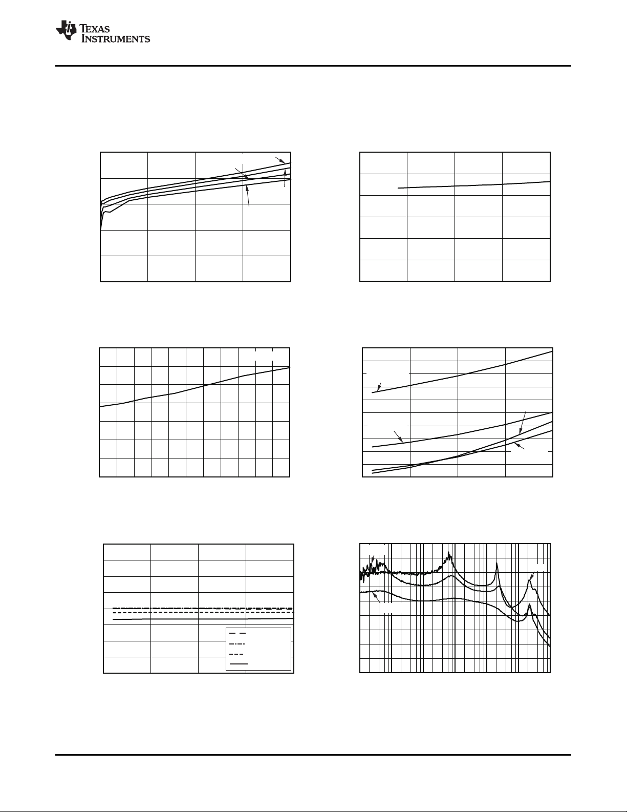
TYPICAL CHARACTERISTICS
= – 40 ° C to +125 ° C), VIN= V
= VIN, C
J
= 1.0 µ F, unless otherwise noted. Typical values are at TJ= +25 ° C.
OUT
= V
EN1
EN2
OUT(TYP)
LINE REGULATION LINE REGULATION
Figure 2. Figure 3.
+ 0.5V or 2.7V, whichever is greater;
www.ti.com
OUTPUT VOLTAGE vs DROPOUT VOLTAGE vs
TEMPERATURE OUTPUT CURRENT
6 Submit Documentation Feedback Copyright © 2007 – 2008, Texas Instruments Incorporated
Figure 4. Figure 5.
Figure 6. Figure 7.
Product Folder Link(s): TPS718xx TPS719xx
200
160
120
80
40
0
0 100 200
I (mA)
OUT
I
( A)m
GND
50 150
T =+125 CJ°
T = 0 CJ-4 °
T =+85 CJ°
T =+25 CJ°
60
50
40
30
20
10
0
I
(
A)m
GND
2.5 5.5 6.5
V (V)
IN
3.5 4.5
I =1mA
OUT
-40 65 125
T ( C)
J
°
5 35-25 -10 20 50 80 95 110
140
120
100
80
60
40
20
0
I
( A)m
GND
I =0mA
OUT
5.0
4.5
4.0
3.5
3.0
2.5
2.0
1.5
1.0
0.5
0
ShutdownCurrent( A)m
T = 40 CJ- °
2.5 5.5 6.5
V (V)
IN
3.5 4.5
T =+125 CJ°
T =+85 CJ°
T =+25 CJ°
450
425
400
375
350
325
300
275
250
CurrentLimit(mA)
2.5 5.5 6.5
V (V)
IN
3.5 4.5
T =+125 C
J
T =+85 C
T =+25 C
T = 40 C
J
J
J
-
°
°
°
°
90
80
70
60
50
40
30
20
10
0
PSRR(dB)
10 100k 10M
Frequency(Hz)
1k
10k100
1M
5mA
100mA
200mA
TPS718xx
TPS719xx
www.ti.com
..................................................................................................................................................... SBVS088C – FEBRUARY 2007 – REVISED MAY 2008
Over operating temperature range (T
I
OUT
= 0.5mA, V
= V
EN1
= VIN, C
EN2
GROUND PIN CURRENT vs GROUND PIN CURRENT vs
OUTPUT CURRENT INPUT VOLTAGE
Figure 8. Figure 9.
GROUND PIN CURRENT vs SHUTDOWN CURRENT vs
TEMPERATURE (BOTH LDOs ENABLED) INPUT VOLTAGE
TYPICAL CHARACTERISTICS (continued)
= – 40 ° C to +125 ° C), V
J
= 1.0 µ F, unless otherwise noted. Typical values are at TJ= +25 ° C.
OUT
= V
IN
OUT(TYP)
+ 0.5V or 2.7V, whichever is greater;
Figure 10. Figure 11.
CURRENT LIMIT vs POWER-SUPPLY RIPPLE REJECTION vs
INPUT VOLTAGE FREQUENCY (V
Copyright © 2007 – 2008, Texas Instruments Incorporated Submit Documentation Feedback 7
Figure 12. Figure 13.
Product Folder Link(s): TPS718xx TPS719xx
– V
IN
= 0.5V)
OUT

80
70
60
50
40
30
20
10
0
V (V)
IN
PSRR (dB)
3.0 4.03.2 3.4 3.6 3.8
V =2.80V
OUT
I =5mA
OUT
10kHz
1kHz
100kHz
1MHz
90
80
70
60
50
40
30
20
10
0
PSRR(dB)
10 100k 10M
Frequency(Hz)
1k
10k100
1M
5mA
100mA
200mA
80
70
60
50
40
30
20
10
0
V (V)
IN
PSRR (dB)
3.0 4.03.2 3.4 3.6 3.8
V =2.80V
I =200mA
OUT
OUT
10kHz
1kHz
100kHz
1MHz
10
1
0.1
0.01
OutputSpectralNoiseDensity( V )
m Hz
Ö
100 10k 100k
Frequency(Hz)
1k
V =2.80V
OUT
10 s/divm
3.3V
6.5V
1V/div
10mV/div
10mV/div
V
IN
V
OUT1
V
OUT2
=1V/ sm
dV
IN
dt
20 s/divm
I
OUT1
V
OUT1
V
OUT2
250mA/div
10mV/div
10mV/div
=200mA/ sm
dI
OUT
dt
I =3mA
OUTmin
TPS718xx
TPS719xx
SBVS088C – FEBRUARY 2007 – REVISED MAY 2008 .....................................................................................................................................................
Over operating temperature range (T
I
OUT
= 0.5mA, V
= V
EN1
= VIN, C
EN2
POWER-SUPPLY RIPPLE REJECTION vs POWER-SUPPLY RIPPLE REJECTION vs
FREQUENCY (V
Figure 14. Figure 15.
POWER-SUPPLY RIPPLE REJECTION vs OUTPUT SPECTRAL NOISE DENSITY vs
INPUT VOLTAGE FREQUENCY
TYPICAL CHARACTERISTICS (continued)
= – 40 ° C to +125 ° C), V
J
= 1.0 µ F, unless otherwise noted. Typical values are at TJ= +25 ° C.
OUT
– V
IN
= 1V) INPUT VOLTAGE
OUT
= V
IN
OUT(TYP)
+ 0.5V or 2.7V, whichever is greater;
www.ti.com
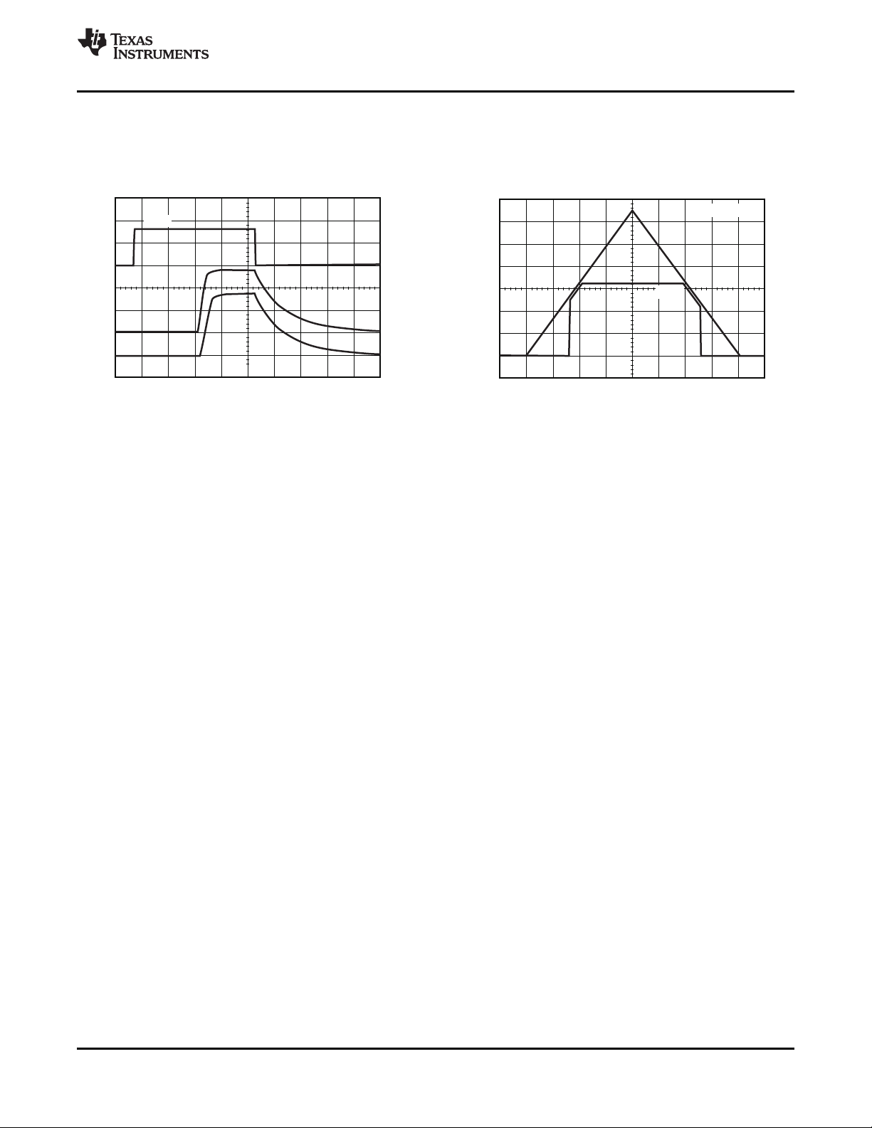
LINE TRANSIENT RESPONSE LOAD TRANSIENT RESPONSE
8 Submit Documentation Feedback Copyright © 2007 – 2008, Texas Instruments Incorporated
Figure 16. Figure 17.
Figure 18. Figure 19.
Product Folder Link(s): TPS718xx TPS719xx
40 s/divm
0V
6.5V
4V/div
1V/div
1V/div
EN1,EN2
V
OUT1
V
OUT2
V
IN
I
OUT
=200mA
V
OUT
1V/div
400ms/div
TPS718xx
TPS719xx
www.ti.com
..................................................................................................................................................... SBVS088C – FEBRUARY 2007 – REVISED MAY 2008
Over operating temperature range (T
I
OUT
= 0.5mA, V
= V
EN1
= VIN, C
EN2
TPS719 ENABLE RESPONSE POWER-UP/POWER-DOWN
Figure 20. Figure 21.
TYPICAL CHARACTERISTICS (continued)
= – 40 ° C to +125 ° C), V
J
= 1.0 µ F, unless otherwise noted. Typical values are at TJ= +25 ° C.
OUT
= V
IN
OUT(TYP)
+ 0.5V or 2.7V, whichever is greater;
Copyright © 2007 – 2008, Texas Instruments Incorporated Submit Documentation Feedback 9
Product Folder Link(s): TPS718xx TPS719xx

TPS718xx
TPS719xx
GND
EN1
EN2
OUT2
IN OUT1
V
IN
V
OUT
V
OUT
1 Fm
1 Fm
1 Fm
2.7V 6.5V- 0.9V 3.6V-
0.9V 3.6V-
On
Off
On
Off
t=3
60 R
L
´
60+R
L
C
OUT
´
TPS718xx
TPS719xx
SBVS088C – FEBRUARY 2007 – REVISED MAY 2008 .....................................................................................................................................................
The TPS718xx/TPS719xx belong to a family of new
generation LDO regulators that use innovative
circuitry to achieve ultra-wide bandwidth and high
loop gain, resulting in extremely high PSRR (up to
1MHz) at very low headroom (V
features, combined with low noise, two independent
enables, low ground pin current and ultra-small
packaging, make this part ideal for portable
applications. This family of regulators offer
sub-bandgap output voltages, current limit and
thermal protection, and is fully specified from – 40 ° C
to +125 ° C.
Figure 22 shows the basic circuit connections.
Figure 22. Typical Application Circuit
Input and Output Capacitor Requirements
Although an input capacitor is not required for
stability, it is good analog design practice to connect
a 0.1 µ F to 1.0 µ F low equivalent series resistance
(ESR) capacitor across the input supply near the
regulator. This capacitor counteracts reactive input
sources and improves transient response, noise
rejection, and ripple rejection. A higher-value
capacitor may be necessary if large, fast rise-time
load transients are anticipated or if the device is
located close to the power source. If source with:
impedance is not sufficiently low, a 0.1 µ F input
capacitor may be necessary to ensure stability.
The TPS718xx/TPS719xx are designed to be stable
with standard ceramic capacitors of values 1.0 µ F or
larger at the output. X5R- and X7R-type capacitors
are best because they have minimal variation in value
and ESR over temperature. Maximum ESR should be
<1.0 Ω .
10 Submit Documentation Feedback Copyright © 2007 – 2008, Texas Instruments Incorporated
www.ti.com
APPLICATION INFORMATION
Board Layout Recommendations to Improve PSRR and Noise Performance
To improve ac performance such as PSRR, output
– V
IN
). These
OUT
noise, and transient response, it is recommended that
the board be designed with separate ground planes
for V
and V
IN
, with each ground plane connected
OUT
only at the GND pin of the device. In addition, the
ground connection for the output capacitor should
connect directly to the GND pin of the device. High
ESR capacitors may degrade PSRR.
Internal Current Limit
The TPS718xx/TPS719xx internal current limits help
protect the regulator during fault conditions. During
current limit, the output sources a fixed amount of
current that is largely independent of output voltage.
For reliable operation, the device should not be
operated in a current limit state for extended periods
of time.
The PMOS pass element in the TPS718xx/TPS719xx
has a built-in body diode that conducts current when
the voltage at OUT exceeds the voltage at IN. This
current is not limited, so if extended reverse voltage
operation is anticipated, external limiting to 5% of
rated output current may be appropriate.
Shutdown
The enable pin (EN) is active high and is compatible
with standard and low voltage, TTL-CMOS levels.
When shutdown capability is not required, EN can be
connected to IN. The TPS719 with internal active
output pulldown circuitry discharges the output with a
time constant ( t) of:
R
= output load resistance
L
C
= output capacitance
OUT
Dropout Voltage
The TPS718xx/TPS719xx use a PMOS pass
transistor to achieve low dropout. When (V
is less than the dropout voltage (V
DO
pass device is in its linear region of operation and the
input-to-output resistance is the R
pass element. V
Product Folder Link(s): TPS718xx TPS719xx
current because the PMOS device behaves like a
resistor in dropout.
approximately scales with output
DO
DS(ON)
– V
IN
)
OUT
), the PMOS
of the PMOS

P =(V V )xI-
D IN OUT OUT
TPS718xx
TPS719xx
www.ti.com
..................................................................................................................................................... SBVS088C – FEBRUARY 2007 – REVISED MAY 2008
As with any linear regulator, PSRR and transient Any tendency to activate the thermal protection circuit
response are degraded as (V
– V
IN
) approaches indicates excessive power dissipation or an
OUT
dropout. This effect is shown in Figure 13 and inadequate heatsink. For reliable operation, junction
Figure 14 in the Typical Characteristics section. temperature should be limited to +125 ° C maximum.
To estimate the margin of safety in a complete design
Transient Response
As with any regulator, increasing the size of the
output capacitor will reduce over/undershoot
magnitude but increase duration of the transient
response.
(including heatsink), increase the ambient
temperature until the thermal protection is triggered;
use worst-case loads and signal conditions. For good
reliability, thermal protection should trigger at least
+35 ° C above the maximum expected ambient
condition of your particular application. This
configuration produces a worst-case junction
Undervoltage Lock-Out (UVLO)
The TPS718xx/TPS719xx utilize an undervoltage
lock-out circuit to keep the output shut off until
internal circuitry is operating properly. The UVLO
circuit has a de-glitch feature so that it typically
ignores undershoot transients on the input if they are
less than 50 µ s duration. On the TPS719xx, the active
pulldown discharges V
when the device is in
OUT
temperature of +125 ° C at the highest expected
ambient temperature and worst-case load.
The internal protection circuitry of the
TPS718xx/TPS719xx has been designed to protect
against overload conditions. It was not intended to
replace proper heatsinking. Continuously running the
TPS718xx/TPS719xx into thermal shutdown
degrades device reliability.
UVLO off condition. However, the input voltage needs
to be greater than 0.8V for active pulldown to work.
Minimum Load
Power Dissipation
The ability to remove heat from the die is different for
each package type, presenting different
The TPS718xx/TPS719xx are stable with no output
load. Traditional PMOS LDO regulators suffer from
lower loop gain at very light output loads. The
TPS718xx/TPS719xx employ an innovative,
low-current mode circuit under very light or no-load
conditions, resulting in improved output voltage
regulation performance down to zero output current.
considerations in the printed circuit board (PCB)
layout. The PCB area around the device that is free
of other components moves the heat from the device
to the ambient air. Performance data for JEDEC lowand high-K boards are given in the Dissipation
Ratings table. Using heavier copper increases the
effectiveness in removing heat from the device. The
addition of plated through-holes to heat-dissipating
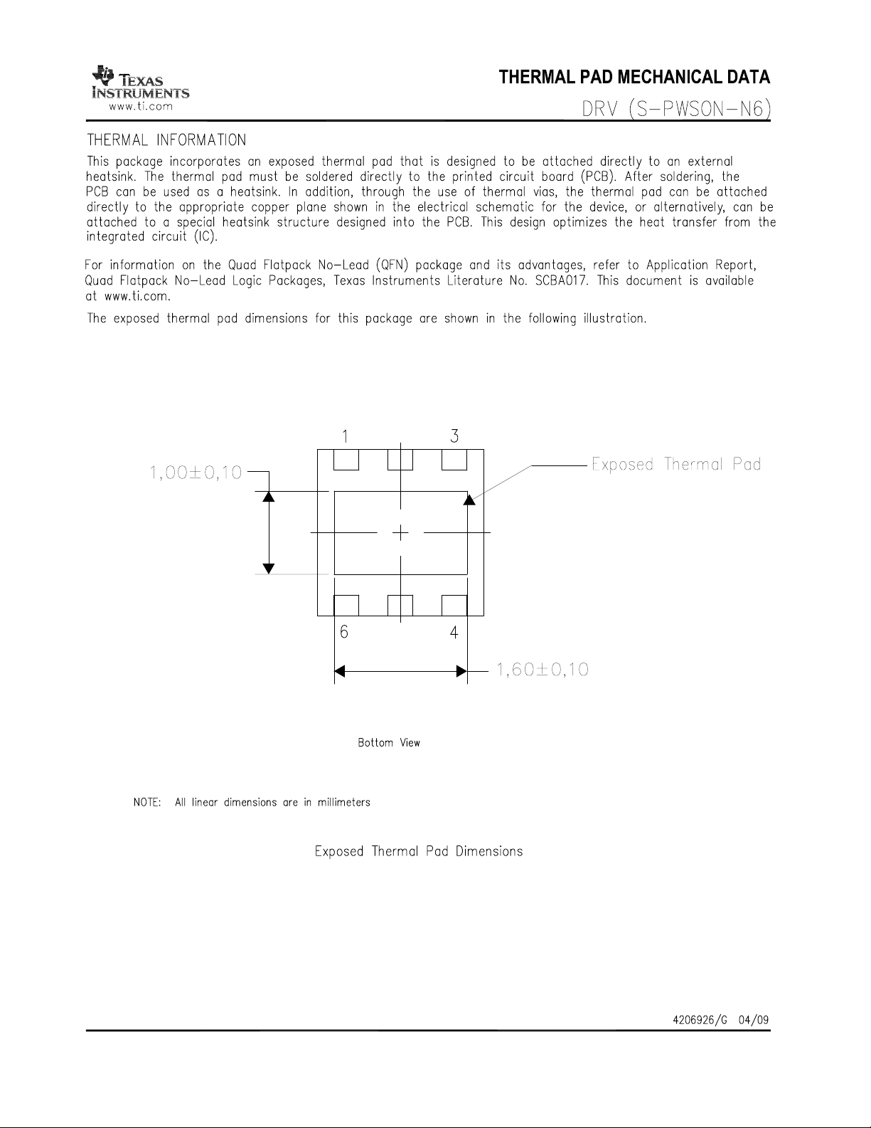
THERMAL INFORMATION
layers also improves the heatsink effectiveness.
Thermal Protection
Thermal protection disables the output when the
junction temperature rises to approximately +160 ° C,
allowing the device to cool. When the junction
Power dissipation depends on input voltage and load
conditions. Power dissipation (P
) is equal to the
D
product of the output current times the voltage drop
across the output pass element (V
to V
IN
shown in Equation 1 :
OUT
temperature cools to approximately +140 ° C the
output circuitry is again enabled. Depending on power
dissipation, thermal resistance, and ambient
temperature, the thermal protection circuit may cycle
Package Mounting
on and off. This cycling limits the dissipation of the Solder pad footprint recommendations for the
regulator, protecting it from damage due to TPS718xx/TPS719xxx are available from the Texas
overheating. Instruments web site at www.ti.com .
Copyright © 2007 – 2008, Texas Instruments Incorporated Submit Documentation Feedback 11
Product Folder Link(s): TPS718xx TPS719xx
), as
(1)

1,690
1,590
1,088
0,988
TPS718xx
TPS719xx
SBVS088C – FEBRUARY 2007 – REVISED MAY 2008 .....................................................................................................................................................
www.ti.com
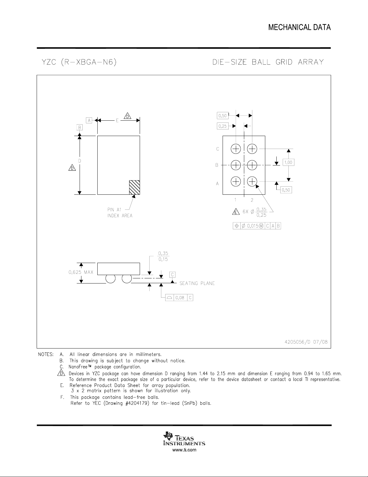
Figure 23. YZC Wafer Chip-Scale Package Dimensions (in mm)
12 Submit Documentation Feedback Copyright © 2007 – 2008, Texas Instruments Incorporated
Product Folder Link(s): TPS718xx TPS719xx

PACKAGE OPTION ADDENDUM
www.ti.com 2-Jul-2009
PACKAGING INFORMATION
Orderable Device Status
TPS71812-33DRVR ACTIVE SON DRV 6 3000 Green (RoHS &
TPS71812-33DRVRG4 ACTIVE SON DRV 6 3000 Green (RoHS &
TPS71812-33DRVT ACTIVE SON DRV 6 250 Green (RoHS &
TPS71812-33DRVTG4 ACTIVE SON DRV 6 250 Green (RoHS &
TPS71818-27YZCR ACTIVE DSBGA YZC 6 3000 Green (RoHS &
TPS71818-27YZCT ACTIVE DSBGA YZC 6 250 Green (RoHS &
TPS71818-33DRVR PREVIEW SON DRV 6 3000 TBD Call TI Call TI
TPS71818-33DRVT PREVIEW SON DRV 6 250 TBD Call TI Call TI
TPS71825-12DRVR ACTIVE SON DRV 6 3000 Green (RoHS &
TPS71825-12DRVT ACTIVE SON DRV 6 250 Green (RoHS &
TPS71828-28YZCR ACTIVE DSBGA YZC 6 3000 Green (RoHS &
TPS71828-28YZCT ACTIVE DSBGA YZC 6 250 Green (RoHS &
TPS71828-30DRVR ACTIVE SON DRV 6 3000 Green (RoHS &
TPS71828-30DRVRG4 ACTIVE SON DRV 6 3000 Green (RoHS &
TPS71828-30DRVT ACTIVE SON DRV 6 250 Green (RoHS &
TPS71828-30DRVTG4 ACTIVE SON DRV 6 250 Green (RoHS &
TPS71913-28DRVR ACTIVE SON DRV 6 3000 Green (RoHS &
TPS71913-28DRVRG4 ACTIVE SON DRV 6 3000 Green (RoHS &
TPS71913-28DRVT ACTIVE SON DRV 6 250 Green (RoHS &
TPS71913-28DRVTG4 ACTIVE SON DRV 6 250 Green (RoHS &
TPS71918-12DRVR ACTIVE SON DRV 6 3000 Green (RoHS &
TPS71918-12DRVRG4 ACTIVE SON DRV 6 3000 Green (RoHS &
TPS71918-12DRVT ACTIVE SON DRV 6 250 Green (RoHS &
TPS71918-12DRVTG4 ACTIVE SON DRV 6 250 Green (RoHS &
TPS71918-13YZCR PREVIEW DSBGA YZC 6 TBD Call TI Call TI
TPS71918-13YZCT PREVIEW DSBGA YZC 6 TBD Call TI Call TI
TPS71918-28DRVR ACTIVE SON DRV 6 3000 Green (RoHS & CU NIPDAU Level-1-260C-UNLIM
(1)
Package
Type
Package
Drawing
Pins Package
Qty
Eco Plan
no Sb/Br)
no Sb/Br)
no Sb/Br)
no Sb/Br)
no Sb/Br)
no Sb/Br)
no Sb/Br)
no Sb/Br)
no Sb/Br)
no Sb/Br)
no Sb/Br)
no Sb/Br)
no Sb/Br)
no Sb/Br)
no Sb/Br)
no Sb/Br)
no Sb/Br)
no Sb/Br)
no Sb/Br)
no Sb/Br)
no Sb/Br)
no Sb/Br)
(2)
Lead/Ball Finish MSL Peak Temp
CU NIPDAU Level-1-260C-UNLIM
CU NIPDAU Level-1-260C-UNLIM
CU NIPDAU Level-1-260C-UNLIM
CU NIPDAU Level-1-260C-UNLIM
SNAGCU Level-1-260C-UNLIM
SNAGCU Level-1-260C-UNLIM
CU NIPDAU Level-1-260C-UNLIM
CU NIPDAU Level-1-260C-UNLIM
SNAGCU Level-1-260C-UNLIM
SNAGCU Level-1-260C-UNLIM
CU NIPDAU Level-1-260C-UNLIM
CU NIPDAU Level-1-260C-UNLIM
CU NIPDAU Level-1-260C-UNLIM
CU NIPDAU Level-1-260C-UNLIM
CU NIPDAU Level-1-260C-UNLIM
CU NIPDAU Level-1-260C-UNLIM
CU NIPDAU Level-1-260C-UNLIM
CU NIPDAU Level-1-260C-UNLIM
CU NIPDAU Level-1-260C-UNLIM
CU NIPDAU Level-1-260C-UNLIM
CU NIPDAU Level-1-260C-UNLIM
CU NIPDAU Level-1-260C-UNLIM
(3)
Addendum-Page 1

PACKAGE OPTION ADDENDUM
www.ti.com 2-Jul-2009
Orderable Device Status
(1)
Package
Type
Package
Drawing
Pins Package
Qty
Eco Plan
(2)
Lead/Ball Finish MSL Peak Temp
no Sb/Br)
TPS71918-28DRVT ACTIVE SON DRV 6 250 Green (RoHS &
CU NIPDAU Level-1-260C-UNLIM
no Sb/Br)
TPS71921-22DRVR ACTIVE SON DRV 6 3000 Green (RoHS &
CU NIPDAU Level-1-260C-UNLIM
no Sb/Br)
TPS71921-22DRVT ACTIVE SON DRV 6 250 Green (RoHS &
CU NIPDAU Level-1-260C-UNLIM
no Sb/Br)
TPS71926-15DRVR ACTIVE SON DRV 6 3000 Green (RoHS &
CU NIPDAU Level-1-260C-UNLIM
no Sb/Br)
TPS71926-15DRVRG4 ACTIVE SON DRV 6 3000 Green (RoHS &
CU NIPDAU Level-1-260C-UNLIM
no Sb/Br)
TPS71926-15DRVT ACTIVE SON DRV 6 250 Green (RoHS &
CU NIPDAU Level-1-260C-UNLIM
no Sb/Br)
TPS71926-15DRVTG4 ACTIVE SON DRV 6 250 Green (RoHS &
CU NIPDAU Level-1-260C-UNLIM
no Sb/Br)
TPS71928-28DRVR ACTIVE SON DRV 6 3000 Green (RoHS &
CU NIPDAU Level-1-260C-UNLIM
no Sb/Br)
TPS71928-28DRVRG4 ACTIVE SON DRV 6 3000 Green (RoHS &
CU NIPDAU Level-1-260C-UNLIM
no Sb/Br)
TPS71928-28DRVT ACTIVE SON DRV 6 250 Green (RoHS &
CU NIPDAU Level-1-260C-UNLIM
no Sb/Br)
TPS71928-28DRVTG4 ACTIVE SON DRV 6 250 Green (RoHS &
CU NIPDAU Level-1-260C-UNLIM
no Sb/Br)
TPS719285-285DRVR ACTIVE SON DRV 6 3000 Green (RoHS &
CU NIPDAU Level-1-260C-UNLIM
no Sb/Br)
TPS719285-285DRVT ACTIVE SON DRV 6 250 Green (RoHS &
CU NIPDAU Level-1-260C-UNLIM
no Sb/Br)
TPS719285-285DSET PREVIEW SON DRV 6 TBD Call TI Call TI
TPS71933-28DRVR ACTIVE SON DRV 6 3000 Green (RoHS &
CU NIPDAU Level-1-260C-UNLIM
no Sb/Br)
TPS71933-28DRVRG4 ACTIVE SON DRV 6 3000 Green (RoHS &
CU NIPDAU Level-1-260C-UNLIM
no Sb/Br)
TPS71933-28DRVT ACTIVE SON DRV 6 250 Green (RoHS &
CU NIPDAU Level-1-260C-UNLIM
no Sb/Br)
TPS71933-28DRVTG4 ACTIVE SON DRV 6 250 Green (RoHS &
CU NIPDAU Level-1-260C-UNLIM
no Sb/Br)
TPS71933-33DRVR ACTIVE SON DRV 6 3000 Green (RoHS &
CU NIPDAU Level-1-260C-UNLIM
no Sb/Br)
TPS71933-33DRVRG4 ACTIVE SON DRV 6 3000 Green (RoHS &
CU NIPDAU Level-1-260C-UNLIM
no Sb/Br)
TPS71933-33DRVT ACTIVE SON DRV 6 250 Green (RoHS &
CU NIPDAU Level-1-260C-UNLIM
no Sb/Br)
TPS71933-33DRVTG4 ACTIVE SON DRV 6 250 Green (RoHS &
CU NIPDAU Level-1-260C-UNLIM
no Sb/Br)
TPS71936-315DRVR ACTIVE SON DRV 6 3000 Green (RoHS &
CU NIPDAU Level-1-260C-UNLIM
no Sb/Br)
TPS71936-315DRVT ACTIVE SON DRV 6 250 Green (RoHS &
CU NIPDAU Level-1-260C-UNLIM
no Sb/Br)
(1)
The marketing status values are defined as follows:
ACTIVE: Product device recommended for new designs.
LIFEBUY: TI has announced that the device will be discontinued, and a lifetime-buy period is in effect.
(3)
Addendum-Page 2

PACKAGE OPTION ADDENDUM
www.ti.com 2-Jul-2009
NRND: Not recommended for new designs. Device is in production to support existing customers, but TI does not recommend using this part in
a new design.
PREVIEW: Device has been announced but is not in production. Samples may or may not be available.
OBSOLETE: TI has discontinued the production of the device.
(2)
Eco Plan - The planned eco-friendly classification: Pb-Free (RoHS), Pb-Free (RoHS Exempt), or Green (RoHS & no Sb/Br) - please check
http://www.ti.com/productcontent for the latest availability information and additional product content details.
TBD: The Pb-Free/Green conversion plan has not been defined.
Pb-Free (RoHS): TI's terms "Lead-Free" or "Pb-Free" mean semiconductor products that are compatible with the current RoHS requirements
for all 6 substances, including the requirement that lead not exceed 0.1% by weight in homogeneous materials. Where designed to be soldered
at high temperatures, TI Pb-Free products are suitable for use in specified lead-free processes.
Pb-Free (RoHS Exempt): This component has a RoHS exemption for either 1) lead-based flip-chip solder bumps used between the die and
package, or 2) lead-based die adhesive used between the die and leadframe. The component is otherwise considered Pb-Free (RoHS
compatible) as defined above.
Green (RoHS & no Sb/Br): TI defines "Green" to mean Pb-Free (RoHS compatible), and free of Bromine (Br) and Antimony (Sb) based flame
retardants (Br or Sb do not exceed 0.1% by weight in homogeneous material)
(3)
MSL, Peak Temp. -- The Moisture Sensitivity Level rating according to the JEDEC industry standard classifications, and peak solder
temperature.
Important Information and Disclaimer:The information provided on this page represents TI's knowledge and belief as of the date that it is
provided. TI bases its knowledge and belief on information provided by third parties, and makes no representation or warranty as to the
accuracy of such information. Efforts are underway to better integrate information from third parties. TI has taken and continues to take
reasonable steps to provide representative and accurate information but may not have conducted destructive testing or chemical analysis on
incoming materials and chemicals. TI and TI suppliers consider certain information to be proprietary, and thus CAS numbers and other limited
information may not be available for release.
In no event shall TI's liability arising out of such information exceed the total purchase price of the TI part(s) at issue in this document sold by TI
to Customer on an annual basis.
Addendum-Page 3

PACKAGE MATERIALS INFORMATION
www.ti.com 1-Jul-2009
TAPE AND REEL INFORMATION
*All dimensions are nominal
Device Package
Type
TPS71812-33DRVR SON DRV 6 3000 179.0 8.4 2.2 2.2 1.2 4.0 8.0 Q2
TPS71812-33DRVT SON DRV 6 250 179.0 8.4 2.2 2.2 1.2 4.0 8.0 Q2
TPS71825-12DRVR SON DRV 6 3000 179.0 8.4 2.2 2.2 1.2 4.0 8.0 Q2
TPS71825-12DRVT SON DRV 6 250 179.0 8.4 2.2 2.2 1.2 4.0 8.0 Q2
TPS71828-30DRVR SON DRV 6 3000 179.0 8.4 2.2 2.2 1.2 4.0 8.0 Q2
TPS71828-30DRVT SON DRV 6 250 179.0 8.4 2.2 2.2 1.2 4.0 8.0 Q2
TPS71913-28DRVR SON DRV 6 3000 179.0 8.4 2.2 2.2 1.2 4.0 8.0 Q2
TPS71913-28DRVT SON DRV 6 250 179.0 8.4 2.2 2.2 1.2 4.0 8.0 Q2
TPS71918-12DRVR SON DRV 6 3000 179.0 8.4 2.2 2.2 1.2 4.0 8.0 Q2
TPS71918-12DRVT SON DRV 6 250 179.0 8.4 2.2 2.2 1.2 4.0 8.0 Q2
TPS71918-28DRVR SON DRV 6 3000 179.0 8.4 2.2 2.2 1.2 4.0 8.0 Q2
TPS71918-28DRVT SON DRV 6 250 179.0 8.4 2.2 2.2 1.2 4.0 8.0 Q2
TPS71921-22DRVR SON DRV 6 3000 179.0 8.4 2.2 2.2 1.2 4.0 8.0 Q2
TPS71921-22DRVT SON DRV 6 250 179.0 8.4 2.2 2.2 1.2 4.0 8.0 Q2
TPS71926-15DRVR SON DRV 6 3000 179.0 8.4 2.2 2.2 1.2 4.0 8.0 Q2
TPS71926-15DRVT SON DRV 6 250 179.0 8.4 2.2 2.2 1.2 4.0 8.0 Q2
TPS71928-28DRVR SON DRV 6 3000 179.0 8.4 2.2 2.2 1.2 4.0 8.0 Q2
TPS71928-28DRVT SON DRV 6 250 179.0 8.4 2.2 2.2 1.2 4.0 8.0 Q2
Package
Drawing
Pins SPQ Reel
Diameter
(mm)
Reel
Width
W1 (mm)
A0 (mm) B0 (mm) K0 (mm) P1
(mm)W(mm)
Pin1
Quadrant
Pack Materials-Page 1

PACKAGE MATERIALS INFORMATION
www.ti.com 1-Jul-2009
Device Package
Type
TPS719285-285DRVR SON DRV 6 3000 179.0 8.4 2.2 2.2 1.2 4.0 8.0 Q2
TPS719285-285DRVT SON DRV 6 250 179.0 8.4 2.2 2.2 1.2 4.0 8.0 Q2
TPS71933-28DRVR SON DRV 6 3000 179.0 8.4 2.2 2.2 1.2 4.0 8.0 Q2
TPS71933-28DRVT SON DRV 6 250 179.0 8.4 2.2 2.2 1.2 4.0 8.0 Q2
TPS71933-33DRVR SON DRV 6 3000 179.0 8.4 2.2 2.2 1.2 4.0 8.0 Q2
TPS71933-33DRVT SON DRV 6 250 179.0 8.4 2.2 2.2 1.2 4.0 8.0 Q2
TPS71936-315DRVR SON DRV 6 3000 179.0 8.4 2.2 2.2 1.2 4.0 8.0 Q2
TPS71936-315DRVT SON DRV 6 250 179.0 8.4 2.2 2.2 1.2 4.0 8.0 Q2
Package
Drawing
Pins SPQ Reel
Diameter
(mm)
Reel
Width
W1 (mm)
A0 (mm) B0 (mm) K0 (mm) P1
(mm)W(mm)
Pin1
Quadrant
*All dimensions are nominal
Device Package Type Package Drawing Pins SPQ Length (mm) Width (mm) Height (mm)
TPS71812-33DRVR SON DRV 6 3000 195.0 200.0 45.0
TPS71812-33DRVT SON DRV 6 250 195.0 200.0 45.0
TPS71825-12DRVR SON DRV 6 3000 195.0 200.0 45.0
TPS71825-12DRVT SON DRV 6 250 195.0 200.0 45.0
TPS71828-30DRVR SON DRV 6 3000 195.0 200.0 45.0
TPS71828-30DRVT SON DRV 6 250 195.0 200.0 45.0
TPS71913-28DRVR SON DRV 6 3000 195.0 200.0 45.0
TPS71913-28DRVT SON DRV 6 250 195.0 200.0 45.0
TPS71918-12DRVR SON DRV 6 3000 195.0 200.0 45.0
Pack Materials-Page 2

PACKAGE MATERIALS INFORMATION
www.ti.com 1-Jul-2009
Device Package Type Package Drawing Pins SPQ Length (mm) Width (mm) Height (mm)
TPS71918-12DRVT SON DRV 6 250 195.0 200.0 45.0
TPS71918-28DRVR SON DRV 6 3000 195.0 200.0 45.0
TPS71918-28DRVT SON DRV 6 250 195.0 200.0 45.0
TPS71921-22DRVR SON DRV 6 3000 195.0 200.0 45.0
TPS71921-22DRVT SON DRV 6 250 195.0 200.0 45.0
TPS71926-15DRVR SON DRV 6 3000 195.0 200.0 45.0
TPS71926-15DRVT SON DRV 6 250 195.0 200.0 45.0
TPS71928-28DRVR SON DRV 6 3000 195.0 200.0 45.0
TPS71928-28DRVT SON DRV 6 250 195.0 200.0 45.0
TPS719285-285DRVR SON DRV 6 3000 195.0 200.0 45.0
TPS719285-285DRVT SON DRV 6 250 195.0 200.0 45.0
TPS71933-28DRVR SON DRV 6 3000 195.0 200.0 45.0
TPS71933-28DRVT SON DRV 6 250 195.0 200.0 45.0
TPS71933-33DRVR SON DRV 6 3000 195.0 200.0 45.0
TPS71933-33DRVT SON DRV 6 250 195.0 200.0 45.0
TPS71936-315DRVR SON DRV 6 3000 195.0 200.0 45.0
TPS71936-315DRVT SON DRV 6 250 195.0 200.0 45.0
Pack Materials-Page 3


IMPORTANT NOTICE
Texas Instruments Incorporated and its subsidiaries (TI) reserve the right to make corrections, modifications, enhancements, improvements,
and other changes to its products and services at any time and to discontinue any product or service without notice. Customers should
obtain the latest relevant information before placing orders and should verify that such information is current and complete. All products are
sold subject to TI’s terms and conditions of sale supplied at the time of order acknowledgment.
TI warrants performance of its hardware products to the specifications applicable at the time of sale in accordance with TI’s standard
warranty. Testing and other quality control techniques are used to the extent TI deems necessary to support this warranty. Except where
mandated by government requirements, testing of all parameters of each product is not necessarily performed.
TI assumes no liability for applications assistance or customer product design. Customers are responsible for their products and
applications using TI components. To minimize the risks associated with customer products and applications, customers should provide
adequate design and operating safeguards.
TI does not warrant or represent that any license, either express or implied, is granted under any TI patent right, copyright, mask work right,
or other TI intellectual property right relating to any combination, machine, or process in which TI products or services are used. Information
published by TI regarding third-party products or services does not constitute a license from TI to use such products or services or a
warranty or endorsement thereof. Use of such information may require a license from a third party under the patents or other intellectual
property of the third party, or a license from TI under the patents or other intellectual property of TI.
Reproduction of TI information in TI data books or data sheets is permissible only if reproduction is without alteration and is accompanied
by all associated warranties, conditions, limitations, and notices. Reproduction of this information with alteration is an unfair and deceptive
business practice. TI is not responsible or liable for such altered documentation. Information of third parties may be subject to additional
restrictions.
Resale of TI products or services with statements different from or beyond the parameters stated by TI for that product or service voids all
express and any implied warranties for the associated TI product or service and is an unfair and deceptive business practice. TI is not
responsible or liable for any such statements.
TI products are not authorized for use in safety-critical applications (such as life support) where a failure of the TI product would reasonably
be expected to cause severe personal injury or death, unless officers of the parties have executed an agreement specifically governing
such use. Buyers represent that they have all necessary expertise in the safety and regulatory ramifications of their applications, and
acknowledge and agree that they are solely responsible for all legal, regulatory and safety-related requirements concerning their products
and any use of TI products in such safety-critical applications, notwithstanding any applications-related information or support that may be
provided by TI. Further, Buyers must fully indemnify TI and its representatives against any damages arising out of the use of TI products in
such safety-critical applications.
TI products are neither designed nor intended for use in military/aerospace applications or environments unless the TI products are
specifically designated by TI as military-grade or "enhanced plastic." Only products designated by TI as military-grade meet military
specifications. Buyers acknowledge and agree that any such use of TI products which TI has not designated as military-grade is solely at
the Buyer's risk, and that they are solely responsible for compliance with all legal and regulatory requirements in connection with such use.
TI products are neither designed nor intended for use in automotive applications or environments unless the specific TI products are
designated by TI as compliant with ISO/TS 16949 requirements. Buyers acknowledge and agree that, if they use any non-designated
products in automotive applications, TI will not be responsible for any failure to meet such requirements.
Following are URLs where you can obtain information on other Texas Instruments products and application solutions:
Products Applications
Amplifiers amplifier.ti.com Audio www.ti.com/audio
Data Converters dataconverter.ti.com Automotive www.ti.com/automotive
DLP® Products www.dlp.com Broadband www.ti.com/broadband
DSP dsp.ti.com Digital Control www.ti.com/digitalcontrol
Clocks and Timers www.ti.com/clocks Medical www.ti.com/medical
Interface interface.ti.com Military www.ti.com/military
Logic logic.ti.com Optical Networking www.ti.com/opticalnetwork
Power Mgmt power.ti.com Security www.ti.com/security
Microcontrollers microcontroller.ti.com Telephony www.ti.com/telephony
RFID www.ti-rfid.com Video & Imaging www.ti.com/video
RF/IF and ZigBee® Solutions www.ti.com/lprf Wireless www.ti.com/wireless
Mailing Address: Texas Instruments, Post Office Box 655303, Dallas, Texas 75265
Copyright © 2009, Texas Instruments Incorporated
 Loading...