

TPS71025
LOW-DROPOUT VOLTAGE REGULATOR
SLVS162A – MAY 1997 – REVISED MAY 1998
1
POST OFFICE BOX 655303 • DALLAS, TEXAS 75265
D
2.5-V Fixed-Output Regulator
D
Very Low-Dropout (LDO) Voltage . . . 57 mV
Typical at I
O
= 100 mA
D
Very Low Quiescent Current, Independent
of Load...292 µA Typ
D
Extremely Low Sleep-State Current,
0.5 µA Max
D
2% Tolerance Over Specified Conditions
D
Output Current Range...0 mA to 500 mA
D
Available in Space Saving 8-Pin SOIC and
20-Pin TSSOP Packages
D
0°C to 125°C Operating Junction
T emperature Range
description
The TPS71025 low-dropout regulator offers an
order of magnitude reduction in both dropout
voltage and quiescent current over conventional
LDO performance. The improvement results from
replacing the typical pnp pass transistor with a
PMOS device.
Because the PMOS device behaves as a low-value resistor, the dropout voltage is very low (maximum of 95 mV
at an output current of 100 mA) and is directly proportional to the output current (see Figure 1). Additionally,
since the PMOS pass element is a voltage-driven device, the quiescent current is very low and remains
independent of output loading (typically 292 µA over the full range of output current, 0 mA to 500 mA). These
two key specifications yield a significant improvement in operating life for battery-powered systems. The
TPS71025 also features a sleep mode; applying a TTL high signal to EN
(enable) shuts down the regulator,
reducing the quiescent current to 0.5 µA maximum at T
J
= 25°C.
AVAILABLE OPTIONS
OUTPUT VOLTAGE
(V)
PACKAGED DEVICES
CHIP FORM
T
J
MIN TYP MAX
SMALL OUTLINE
(D)
PLASTIC DIP
(P)
TSSOP
(PW)
(Y)
0°C to 125°C 2.45 2.5 2.55 TPS71025D TPS71025P TPS71025PWLE TPS71025Y
The D package is availabe taped and reeled. Add R suffix to device type (e.g., TPS71025DR). The PW package is only available left-end taped
and reeled and is indicated by the LE suffix on the device type.
NC – No internal connection
1
2
3
4
8
7
6
5
GND
EN
IN
IN
NC
SENSE
OUT
OUT
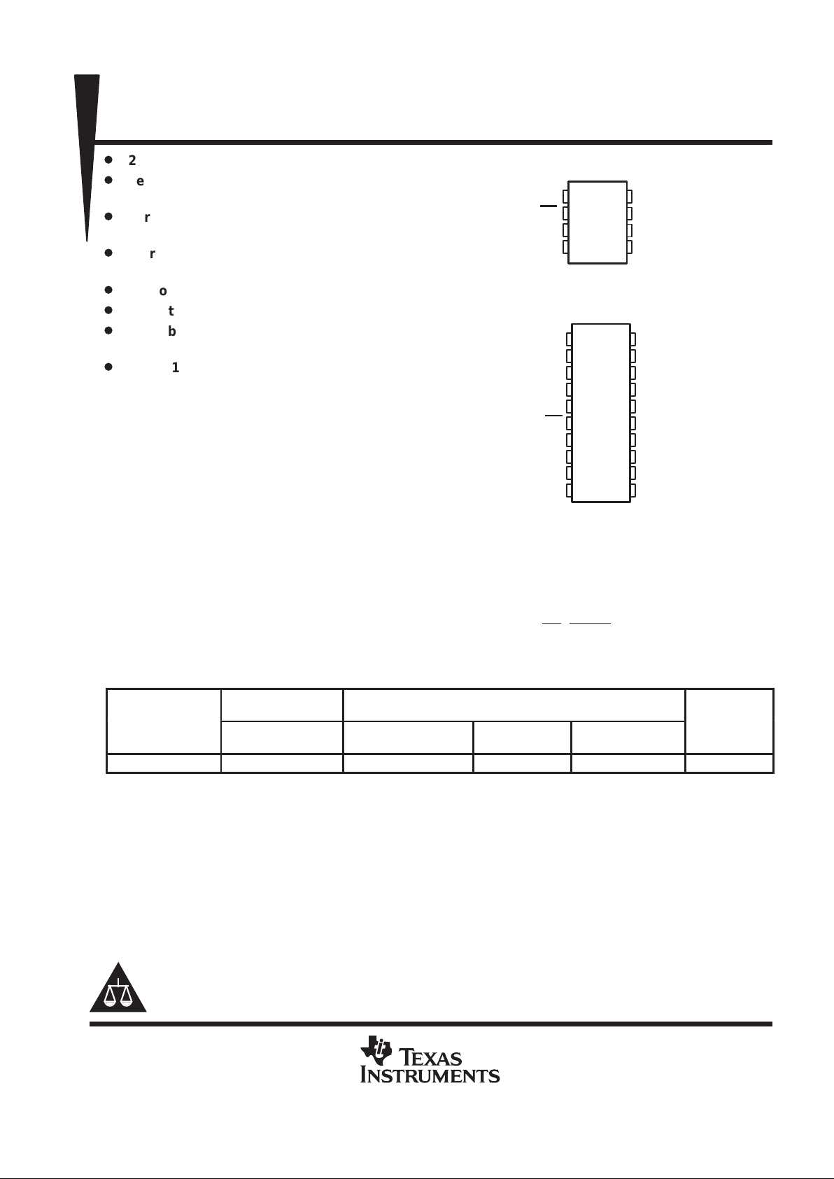
D OR P PACKAGE
(TOP VIEW)
1
2
3
4
5
6
7
8
9
10
20
19
18
17
16
15
14
13
12
11
GND
GND
GND
NC
NC
EN
NC
IN
IN
IN
NC
NC
NC
NC
NC
SENSE
OUT
OUT
NC
NC
PW PACKAGE
(TOP VIEW)
Copyright 1997, Texas Instruments Incorporated
PRODUCTION DATA information is current as of publication date.
Products conform to specifications per the terms of Texas Instruments
standard warranty. Production processing does not necessarily include
testing of all parameters.
Please be aware that an important notice concerning availability, standard warranty, and use in critical applications of
Texas Instruments semiconductor products and disclaimers thereto appears at the end of this data sheet.
TPS71025
LOW-DROPOUT VOLTAGE REGULATOR
SLVS162A – MAY 1997 – REVISED MAY 1998
2
POST OFFICE BOX 655303 • DALLAS, TEXAS 75265
0.2
0.1
0
0 0.05 0.1 0.15 0.2 0.25 0.3
Dropout Voltage – V
0.3
0.4
0.5
0.35 0.4 0.45 0.5
TA = 25°C
IO – Output Current – A
Figure 1. Dropout Voltage Versus Output Current
functional block diagram
_
+
††
V
ref
= 1.182 V
IN
EN
GND
OUT
SENSE
260 kΩ
233 kΩ
†
Switch positions are shown with EN
low (active).
TPS71025
LOW-DROPOUT VOLTAGE REGULATOR
SLVS162A – MAY 1997 – REVISED MAY 1998
3
POST OFFICE BOX 655303 • DALLAS, TEXAS 75265
Terminal Functions
TERMINAL
NO.
DESCRIPTION
NAME
D or P PW
EN 2 6 Enable input. Logic low enables output
GND 1 1–3 Ground
IN 3, 4 8–10 Input supply voltage
OUT 5, 6 13, 14 Output voltage
SENSE 7 15 Output voltage sense input
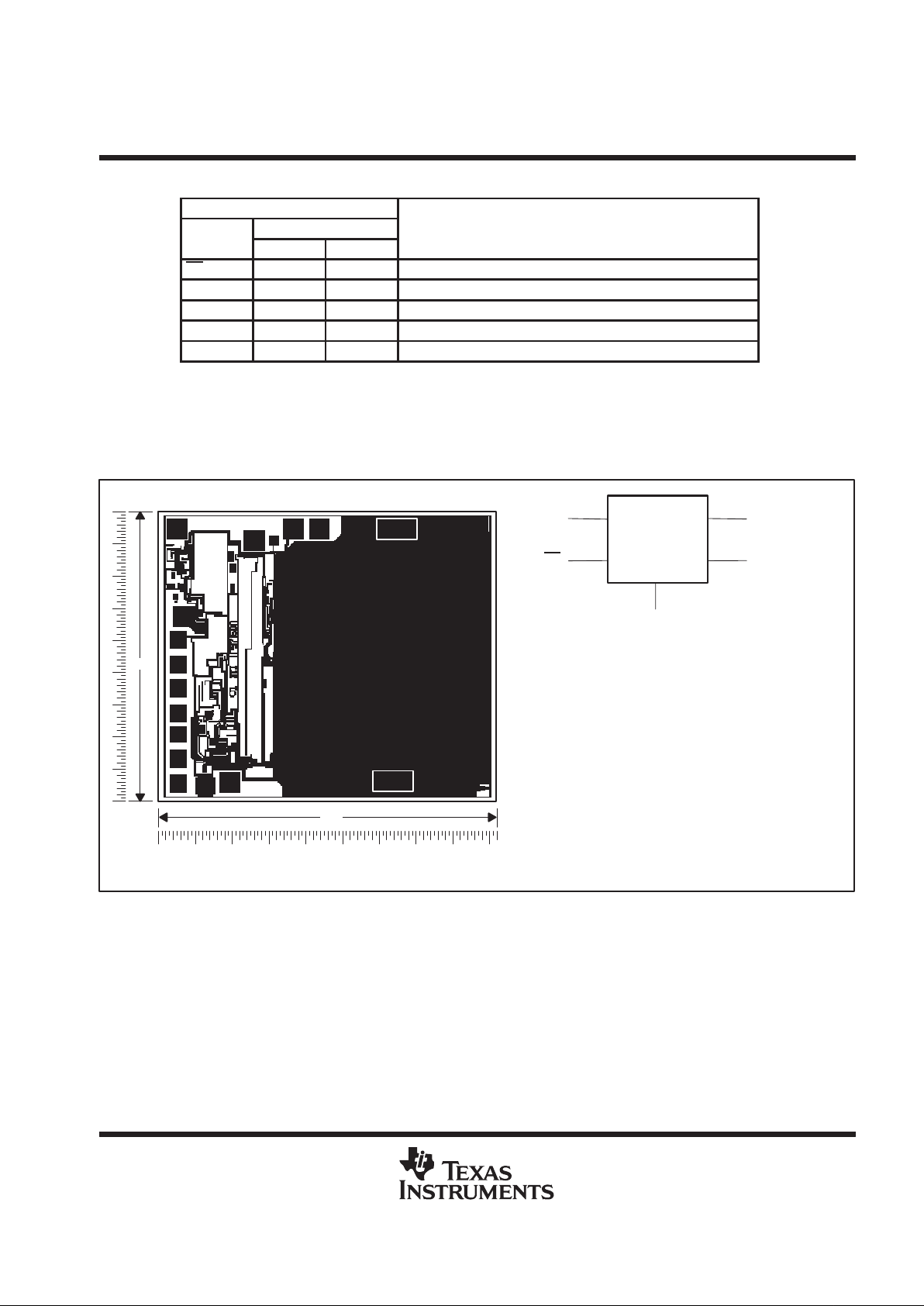
TPS71025Y chip information
These chips, when properly assembled, display characteristics similar to those of the TPS71025. Thermal
compression or ultrasonic bonding may be used on the doped aluminum bonding pads. The chips may be
mounted with conductive epoxy or a gold-silicon preform.
(4)
(3)
(2)
(1)
GND
OUT
IN
EN
TPS71025
80
92
CHIP THICKNESS: 15 MILS TYPICAL
BONDING PADS: 4 × 4 MILS MINIMUM
TJmax = 150°C
TOLERANCES ARE ±10%.
ALL DIMENSIONS ARE IN MILS.
(2)
(5)
(4)
(3)
(1)
BONDING PAD ASSIGNMENTS
SENSE
(5)
NOTE A: For most applications, OUT and SENSE should
be tied together as close as possible to the device;
for other implementations, refer to SENSE-pin
connection discussion in the Application
Information section of this data sheet.
TPS71025
LOW-DROPOUT VOLTAGE REGULATOR
SLVS162A – MAY 1997 – REVISED MAY 1998
4
POST OFFICE BOX 655303 • DALLAS, TEXAS 75265
absolute maximum ratings over operating free-air temperature range (unless otherwise noted)
†
Input voltage range, V
I
, EN (see Note 1) –0.3 V to 11 V. . . . . . . . . . . . . . . . . . . . . . . . . . . . . . . . . . . . . . . . . . . . .
Continuous output current, I
O
2 A. . . . . . . . . . . . . . . . . . . . . . . . . . . . . . . . . . . . . . . . . . . . . . . . . . . . . . . . . . . . . . . . .
Continuous total power dissipation See Dissipation Rating Tables 1 and 2. . . . . . . . . . . . . . . . . . . . . . . . . . . . .
Operating virtual junction temperature range, T
J
–0°C to 150°C. . . . . . . . . . . . . . . . . . . . . . . . . . . . . . . . . . . . . .
Storage temperature range, T
stg
–65°C to 150°C. . . . . . . . . . . . . . . . . . . . . . . . . . . . . . . . . . . . . . . . . . . . . . . . . . .
Lead temperature 1,6 mm (1/16 inch) from case for 10 seconds 260°C. . . . . . . . . . . . . . . . . . . . . . . . . . . . . . .
†
Stresses beyond those listed under “absolute maximum ratings” may cause permanent damage to the device. These are stress ratings only, and
functional operation of the device at these or any other conditions beyond those indicated under “recommended operating conditions” is not
implied. Exposure to absolute-maximum-rated conditions for extended periods may affect device reliability.
NOTE 1: All voltage values are with respect to GND
DISSIPATION RA TING TABLE 1 – FREE-AIR TEMPERATURE
‡
PACKAGE
TA ≤ 25°C
POWER RATING
DERATING FACTOR
ABOVE TA = 25°C
TA = 70°C
POWER RATING
TA = 125°C
POWER RATING
D 725 mW 5.8 mW/°C 464 mW 145 mW
P 1175 mW 9.4 mW/°C 752 mW 235 mW
PW 700 mW 5.6 mW/°C 448 mW 140 mW
DISSIPATION RA TING TABLE 2 – CASE TEMPERATURE
‡
T
≤ 25°C DERATING FACTOR T
= 70°C T
= 125°C
PACKAGE
C
POWER RATING ABOVE TC = 25°CCPOWER RATINGCPOWER RATING
D 2188 mW 17.5 mW/°C 1400 mW 438 mW
P 2738 mW 21.9 mW/°C 1752 mW 548 mW
PW 4025 mW 32.2 mW/°C 2576 mW 805 mW
‡
Dissipation rating tables and figures are provided for maintenance of junction temperature at or below
absolute maximum temperature of 150°C. For guidelines on maintaining junction temperature within
recommended operating range, see the Thermal Information section.
recommended operating conditions
MIN MAX UNIT
Input voltage, V
I
2.97 10 V
High-level input voltage at EN, V
IH
2 V
Low-level input voltage at EN, V
IL
0 0.5 V
Output current range, I
O
0 500 mA
Operating virtual junction temperature range, T
J
0 125 °C
TPS71025
LOW-DROPOUT VOLTAGE REGULATOR
SLVS162A – MAY 1997 – REVISED MAY 1998
5
POST OFFICE BOX 655303 • DALLAS, TEXAS 75265
electrical characteristics over recommended operating junction temperature range, V
I(IN)
= 3.5 V,
I
O
= 10 mA, EN = 0 V, Co = 4.7 µF/CSR† = 1 Ω, SENSE shorted to OUT (unless otherwise noted)
PARAMETER
TEST CONDITIONS
‡
T
J
MIN TYP MAX
UNIT
p
25°C 2.5
Output voltage
3.5 V ≤ V
I
≤ 10
V
0°C to 125°C 2.45 2.55
V
25°C 5.7 7.5
I
O
= 10 mA,
V
I
= 2.45
V
0°C to 125°C 10
p
25°C 57 95
Dropout voltage
I
O
=
100 mA
,
V
I
= 2.45
V
0°C to 125°C 105
mV
25°C 330 450
I
O
=
500 mA
,
V
I
= 2.45
V
0°C to 125°C 500
25°C 0.66 0.9
Pass-element series resistance
0°C to 125°C 1
Ω
p
VI = 3.5 V to 10 V,
25°C 7 23
Input regulation
I
50 µA ≤ IO ≤ 500 mA
0°C to 125°C 12.7 29
mV
IO = 5 mA to 500 mA,
25°C 18 38
p
O
3.5 V ≤ VI ≤ 10 V
0°C to 125°C 75
mV
Output regulation
IO = 50 µA to 500 mA,
25°C 24 60
O
µ
3.5 V ≤ VI ≤ 10 V
0°C to 125°C 120
mV
25°C 43 53
pp
f
=
120 H
z,
I
O
= 50 µ
A
0°C to 125°C 40
Ripple rejection
25°C 39 51
dB
f
=
120 H
z,
I
O
=
500 mA
0°C to 125°C 36
Output noise-spectral density f = 120 Hz 25°C 2
µV/√Hz
Co = 4.7 µF
25°C 274
Output noise voltage
10 H
z ≤ f ≤
100 kH
z,
=
Co = 10 µF
25°C 228
µVrms
CSR = 1 Ω
Co = 100 µF
25°C 159
EN ≤ 0.5 V ,
25°C 292 390
Quiescent current (active mode)
,
0 mA ≤ IO ≤ 500 mA
0°C to 125°C 540
µ
A
pp
25°C 18 475
Supply current (standby mode)
EN
=
V
I
,
2.7 V ≤ V
I
≤ 10
V
0°C to 125°C 1900
nA
p
25°C 1.07 2
Output current limit
V
O
= 0,
V
I
= 10
V
0°C to 125°C 2
A
Pass-element leakage current in standby
25°C 0.223 0.5
gy
mode
EN
=
V
I
,
2.7 V ≤ V
I
≤ 10
V
0°C to 125°C 1
µ
A
Output voltage temperature coefficient 0°C to 125°C 61 75 ppm/°C
Thermal shutdown junction temperature 165 °C
p
2.5 V ≤ VI ≤ 6 V 25°C 2
Logic high input voltage (standby mode), EN
6 V ≤ VI ≤ 10 V 0°C to 125°C 2.7
V
p
25°C 0.5
Logic low input voltage (active mode), EN
2.7 V ≤ V
I
≤ 10
V
0°C to 125°C 0.5
V
Hysteresis voltage, EN 0°C to 125°C 50 mV
p
25°C –0.5 0.5
Input current, EN
0 V ≤ V
I
≤ 10 V
0°C to 125°C –0.5 0.5
µ
A
Input voltage, minimum for active pass
25°C 2 2.5
g,
element
0°C to 125°C 2.5
V
†
CSR (compensation series resistance) refers to the total series resistance, including the equivalent series resistance (ESR) of the capacitor, any
series resistance added externally , and PWB trace resistance to Co.
‡
Pulse-testing techniques are used to maintain virtual junction temperature as close as possible to ambient temperature; thermal effects must
be taken into account separately.
TPS71025
LOW-DROPOUT VOLTAGE REGULATOR
SLVS162A – MAY 1997 – REVISED MAY 1998
6
POST OFFICE BOX 655303 • DALLAS, TEXAS 75265
electrical characteristics at TJ = 25°C, V
I(IN)
= 3.5 V, IO = 10 mA, EN = 0 V, Co = 4.7 µF/CSR† = 1 Ω,
SENSE shorted to OUT (unless otherwise noted)
TPS71025Y
PARAMETER
TEST CONDITIONS
‡
MIN TYP MAX
UNIT
Output voltage 3.5 V ≤ VI ≤ 10 V 2.5 V
IO = 10 mA, VI = 2.45 V 5.7
Dropout voltage
IO = 100 mA, VI = 2.45 V 57
mV
IO = 500 mA, VI = 2.45 V 330
Pass-element series resistance 0.66 Ω
Input regulation VI = 3.5 V to 10 V 7 mV
p
IO = 5 mA to 500 mA 18 mV
Output regulation
IO = 50 µA to 500 mA 24 mV
pp
f = 120 Hz, IO = 50 µA 53
Ripple rejection
f = 120 Hz, IO = 500 mA 51
dB
Output noise-spectral density f = 120 Hz 2
µV/√Hz
Co = 4.7 µF
274
Output noise voltage
10 Hz ≤ f ≤ 100 kHz,
=
Co = 10 µF
228
µVrms
CSR = 1 Ω
Co = 100 µF
159
Quiescent current (active mode)
EN = 0 V,
0 mA ≤ IO ≤ 500 mA
292 µA
Supply current (standby mode) EN = VI, 2.7 V ≤ VI ≤ 10 V 18 nA
Output current limit VO = 0, VI = 10 V 1.07 A
Pass-element leakage current in standby mode EN = VI, 2.7 V ≤ VI ≤ 10 V 0.223 µA
Output voltage temperature coefficient 61 ppm/°C
Thermal shutdown junction temperature 165 °C
2.5 V ≤ VI ≤ 6 V 2
Logic high i
nput voltage (standby mode),
EN
6 V ≤ VI ≤ 10 V 2.7
V
Logic low input voltage (active mode), EN 2.7 V ≤ VI ≤ 10 V 0.5 V
Hysteresis voltage, EN 50 mV
Input current, EN 0 V ≤ VI ≤ 10 V 0 µA
Input voltage, minimum for active pass element 2 V
†
CSR (compensation series resistance) refers to the total series resistance, including the equivalent series resistance (ESR) of the capacitor ,
any series resistance added externally, and PWB trace resistance to Co.
‡
Pulse-testing techniques are used to maintain virtual junction temperature as close as possible to ambient temperature; thermal effects must
be taken into account separately.

TPS71025
LOW-DROPOUT VOLTAGE REGULATOR
SLVS162A – MAY 1997 – REVISED MAY 1998
7
POST OFFICE BOX 655303 • DALLAS, TEXAS 75265
TYPICAL CHARACTERISTICS
Figure 2
2.5
2.49
2.47
2.45
0255075
– Output Voltage – V
2.53
2.54
OUTPUT VOLTAGE
vs
FREE-AIR TEMPERATURE
2.55
100 125
2.52
2.51
2.48
2.46
V
O
TA – Free-Air Temperature – °C
VI = 3.5 V
IO = 10 mA
IO = 500 mA
0.2
0.15
0.1
0
0255075
Drpoout Voltage – V
0.3
0.35
DROPOUT VOLTAGE
vs
FREE-AIR TEMPERATURE
0.4
100 125
0.25
0.05
VI = 2.45 V
IO = 500 mA
IO = 100 mA
IO = 10 mA
TA – Free-Air Temperature – °C
Figure 3
Figure 4
2.5
2.49
2.47
2.45
0255075
– Output Voltage – V
2.52
2.54
OUTPUT VOLTAGE
vs
FREE-AIR TEMPERATURE
2.55
100 125
2.53
2.51
2.48
2.46
IO = 5 mA
V
O
TA – Free-Air Temperature – °C
Figure 5
2.5
2.49
2.48
2.45
3.5 4 4.5 5.5 6 6.5 7.5
2.53
2.54
OUTPUT VOLTAGE
vs
INPUT VOLTAGE
2.55
8 8.5 9.5 10
2.52
2.51
2.47
2.46
57 9
V
O
– Output Voltage – V
VI – Input Voltage – V
TA = 25°C
IO = 500 mA

TPS71025
LOW-DROPOUT VOLTAGE REGULATOR
SLVS162A – MAY 1997 – REVISED MAY 1998
8
POST OFFICE BOX 655303 • DALLAS, TEXAS 75265
TYPICAL CHARACTERISTICS
Figure 6
2.5
2.49
2.47
2.45
0 100 200 300
– Output Voltage – V
2.53
2.54
OUTPUT VOLTAGE
vs
OUTPUT CURRENT
2.55
400 500
2.52
2.51
2.48
2.46
VI = 10 V
VI = 3.5 V
V
O
IO – Output Current – mA
1
0.1
0 50 100 150 200 250 300
TYPICAL REGIONS OF STABILITY
COMPENSATION SERIES RESISTANCE
vs
OUTPUT CURRENT
350 400 450 500
10
100
IO – Output Current – mA
Region of Instability
Region of Instability
VI = 3.5 V
No Input Capacitance
Co = 4.7 µF
No Added Ceramic Capacitance
TA = 25°C
Compensation Series Resistance – Ω
CSR –
Figure 7
1
0.1
0 50 100 150 200 250 300 350 400 450 500
10
100
IO – Output Current – mA
Region of Instability
Region of Instability
VI = 3.5 V
No Input Capacitance
Co = 4.7 µF + 0.5 µF of
Ceramic Capacitance
TA = 25°C
TYPICAL REGIONS OF STABILITY
COMPENSATION SERIES RESISTANCE
vs
OUTPUT CURRENT
Compensation Series Resistance – ΩCSR –
Figure 8
1
0.1
0 0.1 0.2 0.3 0.4 0.5 0.6 0.7 0.8 0.9 1
10
100
Added Ceramic Capacitance – µF
Region of Instability
Region of Instability
TYPICAL REGIONS OF STABILITY
COMPENSATION SERIES RESISTANCE
vs
ADDED CERAMIC CAPACITANCE
VI = 3.5 V
No Input Capacitance
IO= 100 mA
Co = 4.7 µF
TA = 25°C
Compensation Series Resistance – ΩCSR –
Figure 9

TPS71025
LOW-DROPOUT VOLTAGE REGULATOR
SLVS162A – MAY 1997 – REVISED MAY 1998
9
POST OFFICE BOX 655303 • DALLAS, TEXAS 75265
TYPICAL CHARACTERISTICS
1
0.1
0 0.1 0.2 0.3 0.4 0.5 0.6 0.7 0.8 0.9 1
10
100
Added Ceramic Capacitance – µF
Region of Instability
Region of Instability
TYPICAL REGIONS OF STABILITY
COMPENSATION SERIES RESISTANCE
vs
ADDED CERAMIC CAPACITANCE
VI = 3.5 V
No Input Capacitance
IO= 500 mA
Co = 4.7 µF
TA = 25°C
Compensation Series Resistance – ΩCSR –
Figure 10
1
0.1
0 50 100 150 200 250 300
TYPICAL REGIONS OF STABILITY
†
COMPENSATION SERIES RESISTANCE
vs
OUTPUT CURRENT
350 400 450 500
10
100
IO – Output Current – mA
Region of Instability
VI = 3.5 V
No Input Capacitance
Co = 10 µF
No Ceramic Capacitance
TA = 25°C
Compensation Series Resistance – ΩCSR –
Figure 11
1
0.1
0 50 100 150 200 250 300
TYPICAL REGIONS OF STABILITY
†
COMPENSATION SERIES RESISTANCE
vs
OUTPUT CURRENT
350 400 450 500
10
100
IO – Output Current – mA
Region of Instability
VI = 3.5 V
No Input Capacitance
Co = 10 µF + 0.5 µF of
Added Ceramic Capacitance
TA = 25°C
Compensation Series Resistance – ΩCSR –
Figure 12
1
0.1
0 0.1 0.2 0.3 0.4 0.5 0.6
TYPICAL REGIONS OF STABILITY
†
COMPENSATION SERIES RESISTANCE
vs
ADDED CERAMIC CAPACITANCE
0.7 0.8 0.9 1
10
100
Added Ceramic Capacitance – µF
Region of Instability
VI = 3.5 V
No Input Capacitance
Co = 10 µF
IO = 100 mA
TA = 25°C
Compensation Series Resistance – ΩCSR –
Figure 13
†
CSR values below 0.1 Ω are not recommended.

TPS71025
LOW-DROPOUT VOLTAGE REGULATOR
SLVS162A – MAY 1997 – REVISED MAY 1998
10
POST OFFICE BOX 655303 • DALLAS, TEXAS 75265
TYPICAL CHARACTERISTICS
1
0.1
0 0.1 0.2 0.3 0.4 0.5 0.6
TYPICAL REGIONS OF STABILITY
†
COMPENSATION SERIES RESISTANCE
vs
ADDED CERAMIC CAPACITANCE
0.7 0.8 0.9 1
10
100
Added Ceramic Capacitance – µF
Region of Instability
VI = 3.5 V
No Input Capacitance
Co = 10 µF
IO = 500 mA
TA = 25°C
Compensation Series Resistance – ΩCSR –
Figure 14
†
CSR values below 0.1 Ω are not recommended.
IN
EN
OUT
SENSE
+
GND
C
o
CSR
C
cer
(see Note A)
R
L
V
I
NOTE A: Ceramic capacitor
To Load
Figure 15. Test Circuit for Typical Regions of Stability (Figures 7 through 14)

TPS71025
LOW-DROPOUT VOLTAGE REGULATOR
SLVS162A – MAY 1997 – REVISED MAY 1998
11
POST OFFICE BOX 655303 • DALLAS, TEXAS 75265
THERMAL INFORMATION
In response to system-miniaturization trends, integrated circuits are being offered in low-profile and fine-pitch
surface-mount packages. Implementation of many of today’s high-performance devices in these packages
requires special attention to power dissipation. Many system-dependent issues such as thermal coupling,
airflow, added heat sinks and convection surfaces, and the presence of other heat-generating components
affect the power-dissipation limits of a given component.
Three basic approaches for enhancing thermal performance are illustrated in this discussion:
D
Improving the power-dissipation capability of the PWB design
D
Improving the thermal coupling of the component to the PWB
D
Introducing airflow in the system
Figure 16 is an example of a thermally enhanced PWB layout for the 20-lead TSSOP package. This layout
involves adding copper on the PWB to conduct heat away from the device. The R
θJA
for this component/board
system is illustrated in Figure 17. The family of curves illustrates the effect of increasing the size of the
copper-heat-sink surface area. The PWB is a standard FR4 board (L × W × H = 3.2 inch × 3.2 inch × 0.062 inch);
the board traces and heat sink area are 1-oz (per square foot) copper.
Copper Heat Sink
1 oz Copper
Figure 16. Thermally Enhanced PWB Layout (Not to Scale) for the 20-Pin TSSOP
Figure 18 shows the thermal resistance for the same system with the addition of a thermally conductive
compound between the body of the TSSOP package and the PWB copper routed directly beneath the device.
The thermal conductivity for the compound used in this analysis is 0.815 W/m × °C.

TPS71025
LOW-DROPOUT VOLTAGE REGULATOR
SLVS162A – MAY 1997 – REVISED MAY 1998
12
POST OFFICE BOX 655303 • DALLAS, TEXAS 75265
THERMAL INFORMATION
Figure 17
110
90
70
50
0 50 100 150 200 250
130
150
THERMAL RESISTANCE, JUNCTION-TO-AMBIENT
vs
AIR FLOW
170
300
190
C/W
°
JAθ
R – Thermal Resistance, Junction-to-Ambient –
0 cm
2
8 cm
2
2 cm
2
4 cm
2
1 cm
2
Component/Board System
20-Lead TSSOP
Air Flow – ft/min
Figure 18
110
90
70
50
0 50 100 150 200 250
130
150
170
300
190
THERMAL RESISTANCE, JUNCTION-TO-AMBIENT
vs
AIR FLOW
0 cm
2
4 cm
2
2 cm
2
8 cm
2
1 cm
2
C/W
°
JAθ
R – Thermal Resistance, Junction-to-Ambient –
Component/Board System
20-Lead TSSOP
Includes Thermally Conductive
Compound Between Body and Board
Air Flow – ft/min
Using these figures to determine the system R
θJA
allows the maximum power-dissipation P
D(max)
limit to be
calculated with the equation:
P
D(max)
+
T
J(max)
*
T
A
R
q
JA(system)
Where
T
J(max)
is the maximum allowable junction temperature (i.e., 150°C absolute maximum or
125°C maximum recommended operating temperature for specified operation).
This limit should then be applied to the internal power dissipated by the TPS71025 regulator. The equation for
calculating total internal power dissipation of the device is:
P
D(total)
+
ǒ
VI*
V
O
Ǔ
IO)ǒVI
I
Q
Ǔ
Because the quiescent current is very low, the second term is negligible, further simplifying the equation to:
P
D(total)
+
ǒ
VI*
V
O
Ǔ
I
O

TPS71025
LOW-DROPOUT VOLTAGE REGULATOR
SLVS162A – MAY 1997 – REVISED MAY 1998
13
POST OFFICE BOX 655303 • DALLAS, TEXAS 75265
THERMAL INFORMATION
For a 20-lead TSSOP /FR4 board system with thermally conductive compound between the board and the
device body, where T
A
= 55°C, airflow = 100 ft /min, and copper heat sink area = 1 cm2, the maximum
power-dissipation limit can be calculated. As indicated in Figure 18, the system R
θJA
is 94°C/W; therefore, the
maximum power-dissipation limit is:
P
D(max)
+
T
J(max)
*
T
A
R
q
JA(system)
+
125 C*55 C
94 CńW
+
745 mW
°
°°
If the system implements a TPS71025 regulator where V
I
= 3.3 V and IO = 385 mA, the internal power dissipation
is:
P
D(total)
+
ǒ
VI*
V
O
Ǔ
IO+
(3.3*2.5) 0.385+308 mW
Comparing P
D(total)
with P
D(max)
reveals that the power dissipation in this example does not exceed the
maximum limit. When it does, one of two corrective actions can be taken. The power-dissipation limit can be
raised by increasing the airflow or the heat-sink area. Alternatively , the internal power dissipation of the regulator
can be lowered by reducing the input voltage or the load current. In either case, the above calculations should
be repeated with the new system parameters.

TPS71025
LOW-DROPOUT VOLTAGE REGULATOR
SLVS162A – MAY 1997 – REVISED MAY 1998
14
POST OFFICE BOX 655303 • DALLAS, TEXAS 75265
APPLICATION INFORMATION
SENSE
OUT
OUT
9
8
6
10
IN
IN
IN
EN
GND
321
15
14
13
V
I
C1
0.1 µF
50 V
CSR
V
O
C
o
10 µF
+
TPS71025
†
†
Capacitor selection is nontrivial. See external capacitor requirements section.
Figure 19. Typical Application Circuit
The TPS71025 low-dropout (LDO) regulator overcomes many of the shortcomings of earlier-generation LDOs,
while adding features such as a power-saving shutdown mode.
device operation
The TPS71025, unlike many other LDOs, features very low quiescent current that remains virtually constant
even with varying loads. Conventional LDO regulators use a pnp-pass element, the base current of which is
directly proportional to the load current through the regulator (I
B
= IC/β). Examination of the data sheets reveals
that those devices are typically specified under near no-load conditions; actual operating currents are much
higher as evidenced by typical quiescent current versus load current curves. The TPS71025 uses a PMOS
transistor to pass current; because the gate of the PMOS element is voltage driven, operating currents are low
and stable over the full load range. The TPS71025 specifications reflect actual performance under load.
Another pitfall associated with the pnp-pass element is its tendency to saturate when the device goes into
dropout. The resulting drop in β forces an increase in I
B
to maintain the load. During power up, this translates
to large start-up currents. Systems with limited supply current may fail to start up. In battery-powered systems,
it means rapid battery discharge when the voltage decays below the minimum required for regulation. The
TPS71025 quiescent current remains low even when the regulator drops out, eliminating both problems.
The TPS71025 also features a shutdown mode that places the output in the high-impedance state (essentially
equal to the feedback-divider resistance) and reduces quiescent current to under 2 µA. If the shutdown feature
is not used, EN
should be tied to ground. Response to an enable transition is quick; regulated output voltage
is reestablished in typically 120 µs.
minimum load requirements
The TPS71025 family is stable even at zero load; no minimum load is required for operation.
SENSE-pin connection
The SENSE pin must be connected to the regulator output for proper functioning of the regulator. Normally , this
connection should be as short as possible; however, the connection can be made near a critical circuit (remote
sense) to improve performance at that point. Internally , SENSE connects to a high-impedance wide-bandwidth
amplifier through a resistor-divider network, and noise pickup feeds through to the regulator output. Routing the
SENSE connection to minimize/avoid noise pickup is essential. Adding an RC network between SENSE and
OUT to filter noise is not recommended because it can cause the regulator to oscillate.

TPS71025
LOW-DROPOUT VOLTAGE REGULATOR
SLVS162A – MAY 1997 – REVISED MAY 1998
15
POST OFFICE BOX 655303 • DALLAS, TEXAS 75265
APPLICATION INFORMATION
external capacitor requirements
An input capacitor is not required; however, a ceramic bypass capacitor (0.047 pF to 0.1 µF) improves load
transient response and noise rejection if the TPS71025 is located more than a few inches from the power supply .
A higher-capacitance electrolytic capacitor may be necessary if large (hundreds of milliamps) load transients
with fast rise times are anticipated.
As with most LDO regulators, the TPS71025 requires an output capacitor for stability. A low-ESR 10-µF
solid-tantalum capacitor connected from the regulator output to ground is sufficient to ensure stability over the
full load range (see Figure 1 1). Adding high-frequency ceramic or film capacitors (such as power-supply bypass
capacitors for digital or analog ICs) can cause the regulator to become unstable unless the ESR of the tantalum
capacitor is less than 1.2 Ω over temperature. Capacitors with published ESR specifications such as the
AVX TPSD106K035R0300 and the Sprague 593D106X0035D2W work well because the maximum ESR at
25°C is 300 mΩ (typically, the ESR in solid-tantalum capacitors increases by a factor of 2 or less when the
temperature drops from 25°C to –40°C). Where component height and/or mounting area is a problem,
physically smaller, 10-µ F devices can be screened for ESR. Figure 7 through Figure 14 show the stable regions
of operation using different values of output capacitance with various values of ceramic load capacitance.
In applications with little or no high-frequency bypass capacitance (< 0.2 µF), the output capacitance can be
reduced to 4.7 µF, provided ESR is maintained between 0.7 and 2.5 Ω. Because minimum capacitor ESR is
seldom if ever specified, it may be necessary to add a 0.5-Ω to 1-Ω resistor in series with the capacitor and limit
ESR to 1.5 Ω maximum. As shown in the ESR graphs (Figure 7 through Figure 14), minimum ESR is not a
problem when using 10-µF or larger output capacitors.
Below is a partial listing of surface-mount capacitors usable with the TPS71025. This information (along with
the ESR graphs, Figure 7 through Figure 14) is included to assist in selection of suitable capacitance for the
application. When necessary to achieve low height requirements along with high output current and/or high
ceramic load capacitance, several higher ESR capacitors can be used in parallel to meet the guidelines above.

TPS71025
LOW-DROPOUT VOLTAGE REGULATOR
SLVS162A – MAY 1997 – REVISED MAY 1998
16
POST OFFICE BOX 655303 • DALLAS, TEXAS 75265
APPLICATION INFORMATION
external capacitor requirements (continued)
All load and temperature conditions with up to 1 µF of added ceramic load capacitance:
PART NO. MFR. V ALUE MAX ESR
†
SIZE (H × L × W)
†
T421C226M010AS Kemet 22 µF, 10 V 0.5 2.8 × 6 × 3.2
593D156X0025D2W Sprague 15 µF, 25 V 0.3 2.8 × 7.3 × 4.3
593D106X0035D2W Sprague 10 µF, 35 V 0.3 2.8 × 7.3 × 4.3
TPSD106M035R0300 AVX 10 µF, 35 V 0.3 2.8 × 7.3 × 4.3
Load < 200 mA, ceramic load capacitance < 0.2 µF, full temperature range:
PART NO. MFR. V ALUE MAX ESR
†
SIZE (H × L × W)
†
592D156X0020R2T Sprague 15 µF, 20 V 1.1 1.2 × 7.2 × 6
595D156X0025C2T Sprague 15 µF, 25 V 1 2.5 × 7.1 × 3.2
595D106X0025C2T Sprague 10 µF, 25 V 1.2 2.5 × 7.1 × 3.2
293D226X0016D2W Sprague 22 µF, 16 V 1.1 2.8 × 7.3 × 4.3
Load < 100 mA, ceramic load capacitance < 0.2 µF, full temperature range:
PART NO. MFR. V ALUE MAX ESR
†
SIZE (H × L × W)
†
195D106X06R3V2T Sprague 10 µF, 6.3 V 1.5 1.3 × 3.5 × 2.7
195D106X0016X2T Sprague 10 µF, 16 V 1.5 1.3 × 7 × 2.7
595D156X0016B2T Sprague 15 µF, 16 V 1.8 1.6 × 3.8 × 2.6
695D226X0015F2T Sprague 22 µF, 15 V 1.4 1.8 × 6.5 × 3.4
695D156X0020F2T Sprague 15 µF, 20 V 1.5 1.8 × 6.5 × 3.4
695D106X0035G2T Sprague 10 µF, 35 V 1.3 2.5 × 7.6 × 2.5
†
Size is in mm. ESR is maximum resistance at 100 kHz and TA = 25°C. Listings are sorted by height.

TPS71025
LOW-DROPOUT VOLTAGE REGULATOR
SLVS162A – MAY 1997 – REVISED MAY 1998
17
POST OFFICE BOX 655303 • DALLAS, TEXAS 75265
MECHANICAL DATA
D (R-PDSO-G**) PLASTIC SMALL-OUTLINE PACKAGE
14 PIN SHOWN
4040047/D 10/96
0.228 (5,80)
0.244 (6,20)
0.069 (1,75) MAX
0.010 (0,25)
0.004 (0,10)
1
14
0.014 (0,35)
0.020 (0,51)
A
0.157 (4,00)
0.150 (3,81)
7
8
0.044 (1,12)
0.016 (0,40)
Seating Plane
0.010 (0,25)
PINS **
0.008 (0,20) NOM
A MIN
A MAX
DIM
Gage Plane
0.189
(4,80)
(5,00)
0.197
8
(8,55)
(8,75)
0.337
14
0.344
(9,80)
16
0.394
(10,00)
0.386
0.004 (0,10)
M
0.010 (0,25)
0.050 (1,27)
0°–8°
NOTES: A. All linear dimensions are in inches (millimeters).
B. This drawing is subject to change without notice.
C. Body dimensions do not include mold flash or protrusion, not to exceed 0.006 (0,15).
D. Falls within JEDEC MS-012

TPS71025
LOW-DROPOUT VOLTAGE REGULATOR
SLVS162A – MAY 1997 – REVISED MAY 1998
18
POST OFFICE BOX 655303 • DALLAS, TEXAS 75265
MECHANICAL DATA
P (R-PDIP-T8) PLASTIC DUAL-IN-LINE PACKAGE
4040082/B 03/95
0.310 (7,87)
0.290 (7,37)
0.010 (0,25) NOM
0.400 (10,60)
0.355 (9,02)
58
41
0.020 (0,51) MIN
0.070 (1,78) MAX
0.240 (6,10)
0.260 (6,60)
0.200 (5,08) MAX
0.125 (3,18) MIN
0.015 (0,38)
0.021 (0,53)
Seating Plane
M
0.010 (0,25)
0.100 (2,54)
0°–15°
NOTES: A. All linear dimensions are in inches (millimeters).
B. This drawing is subject to change without notice.
C. Falls within JEDEC MS-001

TPS71025
LOW-DROPOUT VOLTAGE REGULATOR
SLVS162A – MAY 1997 – REVISED MAY 1998
19
POST OFFICE BOX 655303 • DALLAS, TEXAS 75265
MECHANICAL DATA
PW (R-PDSO-G**) PLASTIC SMALL-OUTLINE PACKAGE
4040064/E 08/96
14 PIN SHOWN
Seating Plane
0,05 MIN
1,20 MAX
1
A
7
14
0,19
4,50
4,30
8
6,20
6,60
0,30
0,75
0,50
0,25
Gage Plane
0,15 NOM
0,65
M
0,10
0°–8°
0,10
PINS **
A MIN
A MAX
DIM
2,90
3,10
8
4,90
5,10
14
6,60
6,404,90
5,10
16
7,70
20
7,90
24
9,60
9,80
28
NOTES: A. All linear dimensions are in millimeters.
B. This drawing is subject to change without notice.
C. Body dimensions do not include mold flash or protrusion not to exceed 0,15.
D. Falls within JEDEC MO-153

IMPORTANT NOTICE
T exas Instruments and its subsidiaries (TI) reserve the right to make changes to their products or to discontinue
any product or service without notice, and advise customers to obtain the latest version of relevant information
to verify, before placing orders, that information being relied on is current and complete. All products are sold
subject to the terms and conditions of sale supplied at the time of order acknowledgement, including those
pertaining to warranty, patent infringement, and limitation of liability.
TI warrants performance of its semiconductor products to the specifications applicable at the time of sale in
accordance with TI’s standard warranty. Testing and other quality control techniques are utilized to the extent
TI deems necessary to support this warranty. Specific testing of all parameters of each device is not necessarily
performed, except those mandated by government requirements.
CERT AIN APPLICATIONS USING SEMICONDUCTOR PRODUCTS MAY INVOLVE POTENTIAL RISKS OF
DEATH, PERSONAL INJURY, OR SEVERE PROPERTY OR ENVIRONMENTAL DAMAGE (“CRITICAL
APPLICATIONS”). TI SEMICONDUCTOR PRODUCTS ARE NOT DESIGNED, AUTHORIZED, OR
WARRANTED TO BE SUITABLE FOR USE IN LIFE-SUPPORT DEVICES OR SYSTEMS OR OTHER
CRITICAL APPLICATIONS. INCLUSION OF TI PRODUCTS IN SUCH APPLICA TIONS IS UNDERST OOD TO
BE FULLY AT THE CUSTOMER’S RISK.
In order to minimize risks associated with the customer’s applications, adequate design and operating
safeguards must be provided by the customer to minimize inherent or procedural hazards.
TI assumes no liability for applications assistance or customer product design. TI does not warrant or represent
that any license, either express or implied, is granted under any patent right, copyright, mask work right, or other
intellectual property right of TI covering or relating to any combination, machine, or process in which such
semiconductor products or services might be or are used. TI’s publication of information regarding any third
party’s products or services does not constitute TI’s approval, warranty or endorsement thereof.
Copyright 1998, Texas Instruments Incorporated
 Loading...