

Texas Instruments TPS71025PWR, TPS71025P, TPS71025PWLE, TPS71025DR, TPS71025D Datasheet
TPS71025
LOW-DROPOUT VOLTAGE REGULATOR
SLVS162A – MAY 1997 – REVISED MAY 1998
1
POST OFFICE BOX 655303 • DALLAS, TEXAS 75265
D
2.5-V Fixed-Output Regulator
D
Very Low-Dropout (LDO) Voltage . . . 57 mV
Typical at I
O
= 100 mA
D
Very Low Quiescent Current, Independent
of Load...292 µA Typ
D
Extremely Low Sleep-State Current,
0.5 µA Max
D
2% Tolerance Over Specified Conditions
D
Output Current Range...0 mA to 500 mA
D
Available in Space Saving 8-Pin SOIC and
20-Pin TSSOP Packages
D
0°C to 125°C Operating Junction
T emperature Range
description
The TPS71025 low-dropout regulator offers an
order of magnitude reduction in both dropout
voltage and quiescent current over conventional
LDO performance. The improvement results from
replacing the typical pnp pass transistor with a
PMOS device.
Because the PMOS device behaves as a low-value resistor, the dropout voltage is very low (maximum of 95 mV
at an output current of 100 mA) and is directly proportional to the output current (see Figure 1). Additionally,
since the PMOS pass element is a voltage-driven device, the quiescent current is very low and remains
independent of output loading (typically 292 µA over the full range of output current, 0 mA to 500 mA). These
two key specifications yield a significant improvement in operating life for battery-powered systems. The
TPS71025 also features a sleep mode; applying a TTL high signal to EN
(enable) shuts down the regulator,
reducing the quiescent current to 0.5 µA maximum at T
J
= 25°C.
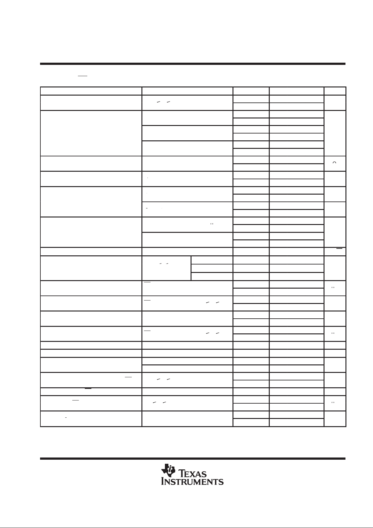
AVAILABLE OPTIONS
OUTPUT VOLTAGE
(V)
PACKAGED DEVICES
CHIP FORM
T
J
MIN TYP MAX
SMALL OUTLINE
(D)
PLASTIC DIP
(P)
TSSOP
(PW)
(Y)
0°C to 125°C 2.45 2.5 2.55 TPS71025D TPS71025P TPS71025PWLE TPS71025Y
The D package is availabe taped and reeled. Add R suffix to device type (e.g., TPS71025DR). The PW package is only available left-end taped
and reeled and is indicated by the LE suffix on the device type.
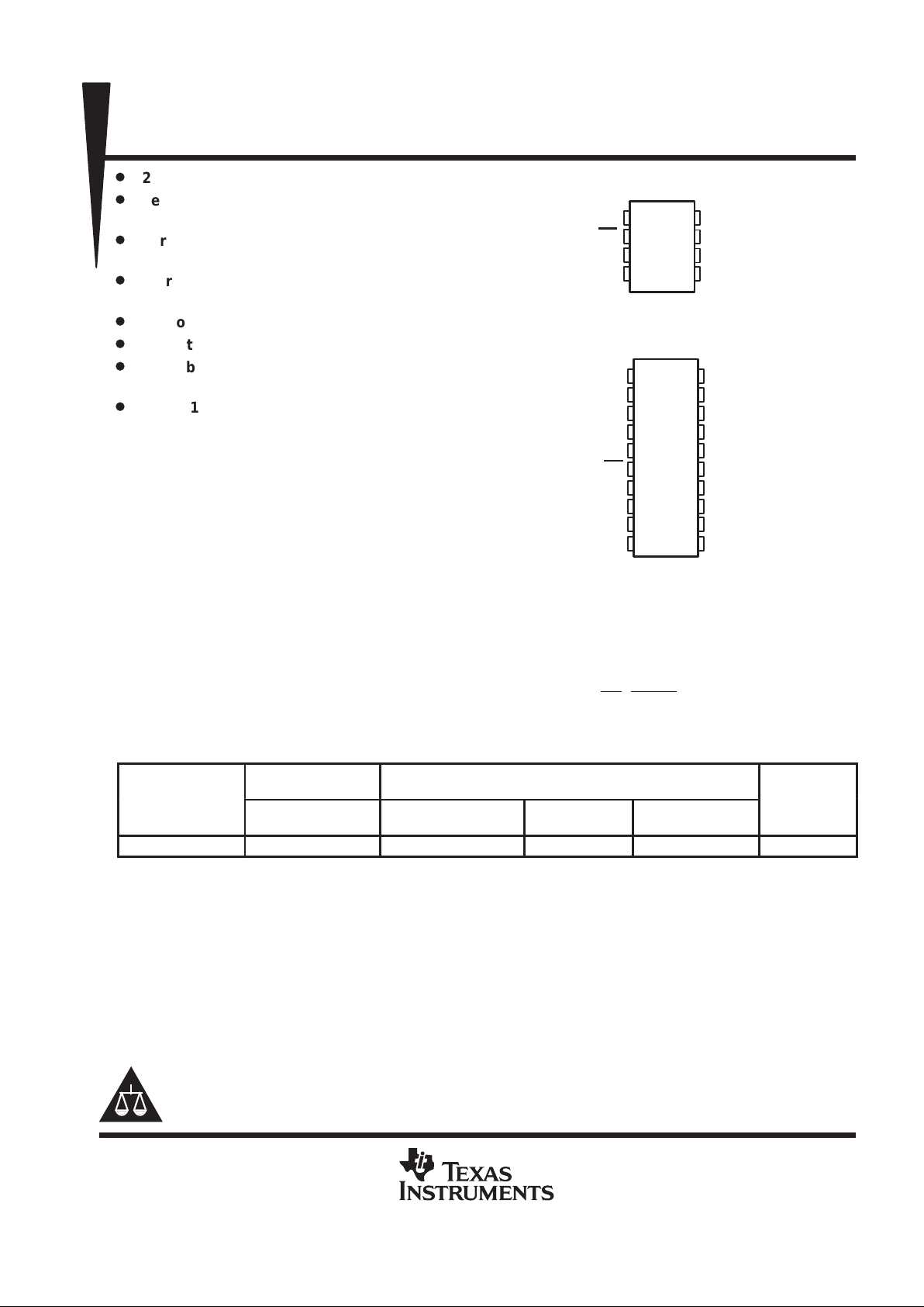
NC – No internal connection
1
2
3
4
8
7
6
5
GND
EN
IN
IN
NC
SENSE
OUT
OUT
D OR P PACKAGE
(TOP VIEW)
1
2
3
4
5
6
7
8
9
10
20
19
18
17
16
15
14
13
12
11
GND
GND
GND
NC
NC
EN
NC
IN
IN
IN
NC
NC
NC
NC
NC
SENSE
OUT
OUT
NC
NC
PW PACKAGE
(TOP VIEW)
Copyright 1997, Texas Instruments Incorporated
PRODUCTION DATA information is current as of publication date.
Products conform to specifications per the terms of Texas Instruments
standard warranty. Production processing does not necessarily include
testing of all parameters.
Please be aware that an important notice concerning availability, standard warranty, and use in critical applications of
Texas Instruments semiconductor products and disclaimers thereto appears at the end of this data sheet.
TPS71025
LOW-DROPOUT VOLTAGE REGULATOR
SLVS162A – MAY 1997 – REVISED MAY 1998
2
POST OFFICE BOX 655303 • DALLAS, TEXAS 75265
0.2
0.1
0
0 0.05 0.1 0.15 0.2 0.25 0.3
Dropout Voltage – V
0.3
0.4
0.5
0.35 0.4 0.45 0.5
TA = 25°C
IO – Output Current – A
Figure 1. Dropout Voltage Versus Output Current
functional block diagram
_
+
††
V
ref
= 1.182 V
IN
EN
GND
OUT
SENSE
260 kΩ
233 kΩ
†
Switch positions are shown with EN
low (active).
TPS71025
LOW-DROPOUT VOLTAGE REGULATOR
SLVS162A – MAY 1997 – REVISED MAY 1998
3
POST OFFICE BOX 655303 • DALLAS, TEXAS 75265
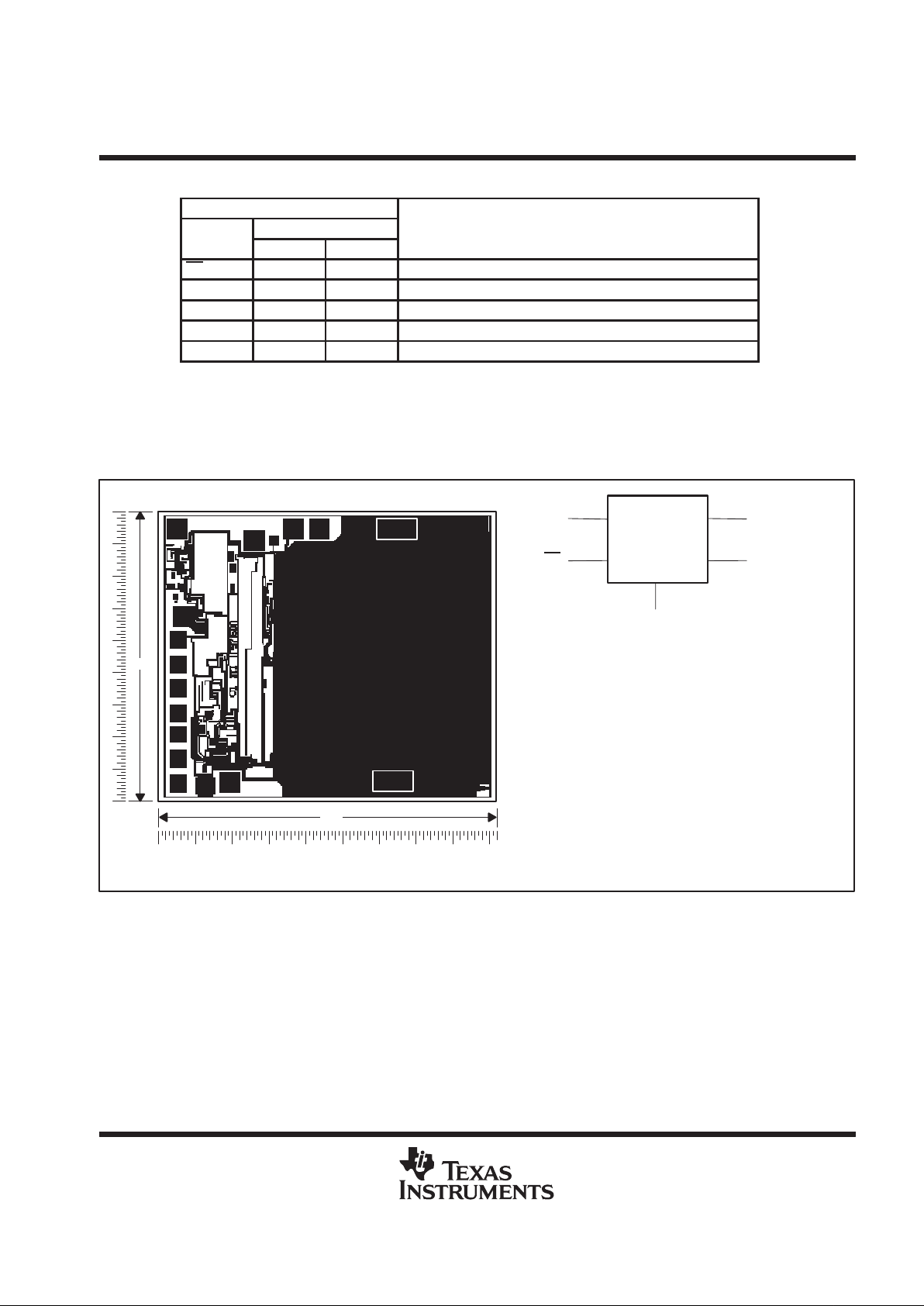
Terminal Functions
TERMINAL
NO.
DESCRIPTION
NAME
D or P PW
EN 2 6 Enable input. Logic low enables output
GND 1 1–3 Ground
IN 3, 4 8–10 Input supply voltage
OUT 5, 6 13, 14 Output voltage
SENSE 7 15 Output voltage sense input
TPS71025Y chip information
These chips, when properly assembled, display characteristics similar to those of the TPS71025. Thermal
compression or ultrasonic bonding may be used on the doped aluminum bonding pads. The chips may be
mounted with conductive epoxy or a gold-silicon preform.
(4)
(3)
(2)
(1)
GND
OUT
IN
EN
TPS71025
80
92
CHIP THICKNESS: 15 MILS TYPICAL
BONDING PADS: 4 × 4 MILS MINIMUM
TJmax = 150°C
TOLERANCES ARE ±10%.
ALL DIMENSIONS ARE IN MILS.
(2)
(5)
(4)
(3)
(1)
BONDING PAD ASSIGNMENTS
SENSE
(5)
NOTE A: For most applications, OUT and SENSE should
be tied together as close as possible to the device;
for other implementations, refer to SENSE-pin
connection discussion in the Application
Information section of this data sheet.
TPS71025
LOW-DROPOUT VOLTAGE REGULATOR
SLVS162A – MAY 1997 – REVISED MAY 1998
4
POST OFFICE BOX 655303 • DALLAS, TEXAS 75265
absolute maximum ratings over operating free-air temperature range (unless otherwise noted)
†
Input voltage range, V
I
, EN (see Note 1) –0.3 V to 11 V. . . . . . . . . . . . . . . . . . . . . . . . . . . . . . . . . . . . . . . . . . . . .
Continuous output current, I
O
2 A. . . . . . . . . . . . . . . . . . . . . . . . . . . . . . . . . . . . . . . . . . . . . . . . . . . . . . . . . . . . . . . . .
Continuous total power dissipation See Dissipation Rating Tables 1 and 2. . . . . . . . . . . . . . . . . . . . . . . . . . . . .
Operating virtual junction temperature range, T
J
–0°C to 150°C. . . . . . . . . . . . . . . . . . . . . . . . . . . . . . . . . . . . . .
Storage temperature range, T
stg
–65°C to 150°C. . . . . . . . . . . . . . . . . . . . . . . . . . . . . . . . . . . . . . . . . . . . . . . . . . .
Lead temperature 1,6 mm (1/16 inch) from case for 10 seconds 260°C. . . . . . . . . . . . . . . . . . . . . . . . . . . . . . .
†
Stresses beyond those listed under “absolute maximum ratings” may cause permanent damage to the device. These are stress ratings only, and
functional operation of the device at these or any other conditions beyond those indicated under “recommended operating conditions” is not
implied. Exposure to absolute-maximum-rated conditions for extended periods may affect device reliability.
NOTE 1: All voltage values are with respect to GND
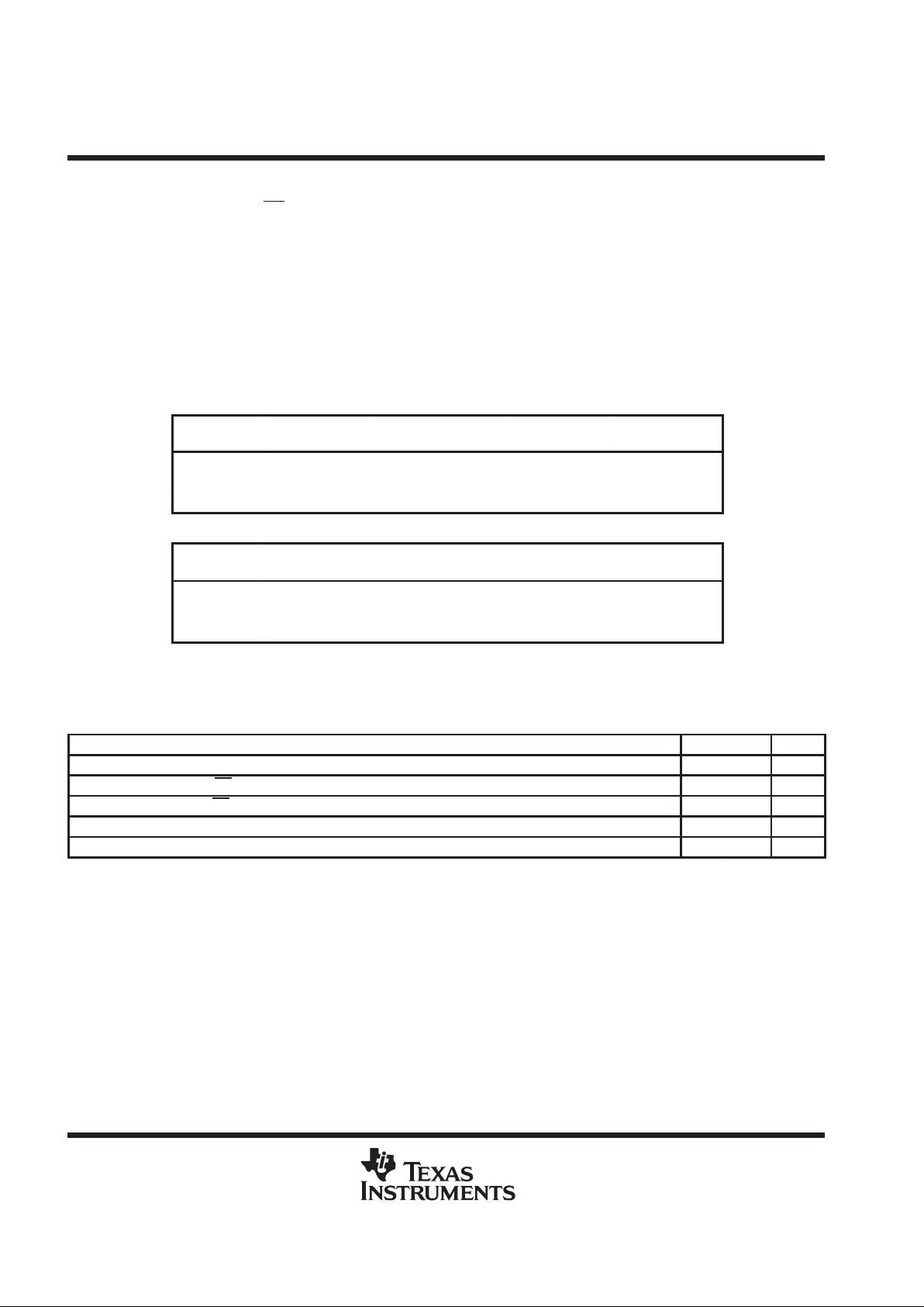
DISSIPATION RA TING TABLE 1 – FREE-AIR TEMPERATURE
‡
PACKAGE
TA ≤ 25°C
POWER RATING
DERATING FACTOR
ABOVE TA = 25°C
TA = 70°C
POWER RATING
TA = 125°C
POWER RATING
D 725 mW 5.8 mW/°C 464 mW 145 mW
P 1175 mW 9.4 mW/°C 752 mW 235 mW
PW 700 mW 5.6 mW/°C 448 mW 140 mW
DISSIPATION RA TING TABLE 2 – CASE TEMPERATURE
‡
T
≤ 25°C DERATING FACTOR T
= 70°C T
= 125°C
PACKAGE
C
POWER RATING ABOVE TC = 25°CCPOWER RATINGCPOWER RATING
D 2188 mW 17.5 mW/°C 1400 mW 438 mW
P 2738 mW 21.9 mW/°C 1752 mW 548 mW
PW 4025 mW 32.2 mW/°C 2576 mW 805 mW
‡
Dissipation rating tables and figures are provided for maintenance of junction temperature at or below
absolute maximum temperature of 150°C. For guidelines on maintaining junction temperature within
recommended operating range, see the Thermal Information section.
recommended operating conditions
MIN MAX UNIT
Input voltage, V
I
2.97 10 V
High-level input voltage at EN, V
IH
2 V
Low-level input voltage at EN, V
IL
0 0.5 V
Output current range, I
O
0 500 mA
Operating virtual junction temperature range, T
J
0 125 °C
TPS71025
LOW-DROPOUT VOLTAGE REGULATOR
SLVS162A – MAY 1997 – REVISED MAY 1998
5
POST OFFICE BOX 655303 • DALLAS, TEXAS 75265
electrical characteristics over recommended operating junction temperature range, V
I(IN)
= 3.5 V,
I
O
= 10 mA, EN = 0 V, Co = 4.7 µF/CSR† = 1 Ω, SENSE shorted to OUT (unless otherwise noted)
PARAMETER
TEST CONDITIONS
‡
T
J
MIN TYP MAX
UNIT
p
25°C 2.5
Output voltage
3.5 V ≤ V
I
≤ 10
V
0°C to 125°C 2.45 2.55
V
25°C 5.7 7.5
I
O
= 10 mA,
V
I
= 2.45
V
0°C to 125°C 10
p
25°C 57 95
Dropout voltage
I
O
=
100 mA
,
V
I
= 2.45
V
0°C to 125°C 105
mV
25°C 330 450
I
O
=
500 mA
,
V
I
= 2.45
V
0°C to 125°C 500
25°C 0.66 0.9
Pass-element series resistance
0°C to 125°C 1
Ω
p
VI = 3.5 V to 10 V,
25°C 7 23
Input regulation
I
50 µA ≤ IO ≤ 500 mA
0°C to 125°C 12.7 29
mV
IO = 5 mA to 500 mA,
25°C 18 38
p
O
3.5 V ≤ VI ≤ 10 V
0°C to 125°C 75
mV
Output regulation
IO = 50 µA to 500 mA,
25°C 24 60
O
µ
3.5 V ≤ VI ≤ 10 V
0°C to 125°C 120
mV
25°C 43 53
pp
f
=
120 H
z,
I
O
= 50 µ
A
0°C to 125°C 40
Ripple rejection
25°C 39 51
dB
f
=
120 H
z,
I
O
=
500 mA
0°C to 125°C 36
Output noise-spectral density f = 120 Hz 25°C 2
µV/√Hz
Co = 4.7 µF
25°C 274
Output noise voltage
10 H
z ≤ f ≤
100 kH
z,
=
Co = 10 µF
25°C 228
µVrms
CSR = 1 Ω
Co = 100 µF
25°C 159
EN ≤ 0.5 V ,
25°C 292 390
Quiescent current (active mode)
,
0 mA ≤ IO ≤ 500 mA
0°C to 125°C 540
µ
A
pp
25°C 18 475
Supply current (standby mode)
EN
=
V
I
,
2.7 V ≤ V
I
≤ 10
V
0°C to 125°C 1900
nA
p
25°C 1.07 2
Output current limit
V
O
= 0,
V
I
= 10
V
0°C to 125°C 2
A
Pass-element leakage current in standby
25°C 0.223 0.5
gy
mode
EN
=
V
I
,
2.7 V ≤ V
I
≤ 10
V
0°C to 125°C 1
µ
A
Output voltage temperature coefficient 0°C to 125°C 61 75 ppm/°C
Thermal shutdown junction temperature 165 °C
p
2.5 V ≤ VI ≤ 6 V 25°C 2
Logic high input voltage (standby mode), EN
6 V ≤ VI ≤ 10 V 0°C to 125°C 2.7
V
p
25°C 0.5
Logic low input voltage (active mode), EN
2.7 V ≤ V
I
≤ 10
V
0°C to 125°C 0.5
V
Hysteresis voltage, EN 0°C to 125°C 50 mV
p
25°C –0.5 0.5
Input current, EN
0 V ≤ V
I
≤ 10 V
0°C to 125°C –0.5 0.5
µ
A
Input voltage, minimum for active pass
25°C 2 2.5
g,
element
0°C to 125°C 2.5
V
†
CSR (compensation series resistance) refers to the total series resistance, including the equivalent series resistance (ESR) of the capacitor, any
series resistance added externally , and PWB trace resistance to Co.
‡
Pulse-testing techniques are used to maintain virtual junction temperature as close as possible to ambient temperature; thermal effects must
be taken into account separately.
TPS71025
LOW-DROPOUT VOLTAGE REGULATOR
SLVS162A – MAY 1997 – REVISED MAY 1998
6
POST OFFICE BOX 655303 • DALLAS, TEXAS 75265
electrical characteristics at TJ = 25°C, V
I(IN)
= 3.5 V, IO = 10 mA, EN = 0 V, Co = 4.7 µF/CSR† = 1 Ω,
SENSE shorted to OUT (unless otherwise noted)
TPS71025Y
PARAMETER
TEST CONDITIONS
‡
MIN TYP MAX
UNIT
Output voltage 3.5 V ≤ VI ≤ 10 V 2.5 V
IO = 10 mA, VI = 2.45 V 5.7
Dropout voltage
IO = 100 mA, VI = 2.45 V 57
mV
IO = 500 mA, VI = 2.45 V 330
Pass-element series resistance 0.66 Ω
Input regulation VI = 3.5 V to 10 V 7 mV
p
IO = 5 mA to 500 mA 18 mV
Output regulation
IO = 50 µA to 500 mA 24 mV
pp
f = 120 Hz, IO = 50 µA 53
Ripple rejection
f = 120 Hz, IO = 500 mA 51
dB
Output noise-spectral density f = 120 Hz 2
µV/√Hz
Co = 4.7 µF
274
Output noise voltage
10 Hz ≤ f ≤ 100 kHz,
=
Co = 10 µF
228
µVrms
CSR = 1 Ω
Co = 100 µF
159
Quiescent current (active mode)
EN = 0 V,
0 mA ≤ IO ≤ 500 mA
292 µA
Supply current (standby mode) EN = VI, 2.7 V ≤ VI ≤ 10 V 18 nA
Output current limit VO = 0, VI = 10 V 1.07 A
Pass-element leakage current in standby mode EN = VI, 2.7 V ≤ VI ≤ 10 V 0.223 µA
Output voltage temperature coefficient 61 ppm/°C
Thermal shutdown junction temperature 165 °C
2.5 V ≤ VI ≤ 6 V 2
Logic high i
nput voltage (standby mode),
EN
6 V ≤ VI ≤ 10 V 2.7
V
Logic low input voltage (active mode), EN 2.7 V ≤ VI ≤ 10 V 0.5 V
Hysteresis voltage, EN 50 mV
Input current, EN 0 V ≤ VI ≤ 10 V 0 µA
Input voltage, minimum for active pass element 2 V
†
CSR (compensation series resistance) refers to the total series resistance, including the equivalent series resistance (ESR) of the capacitor ,
any series resistance added externally, and PWB trace resistance to Co.
‡
Pulse-testing techniques are used to maintain virtual junction temperature as close as possible to ambient temperature; thermal effects must
be taken into account separately.
 Loading...