

TEXAS INSTRUMENTS TPS61161, TPS61160 Technical data
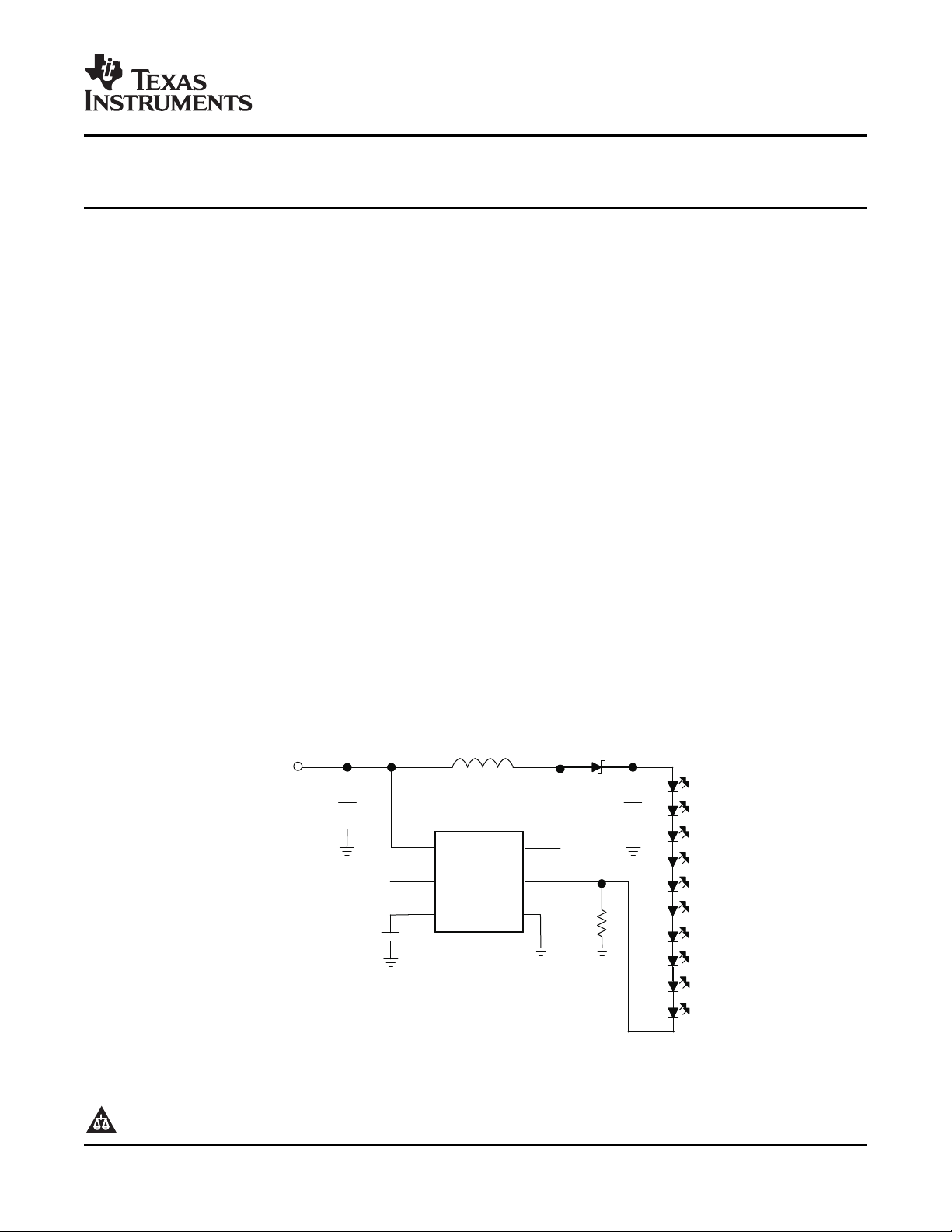
C1
D1
VIN SW
FB
GND
CTRL
COMP
C2
20mA
TPS61161
ON/OFF
DIMMING
CONTROL
V 3Vto18V
I
L1
22 Hm
1 Fm
C3
220nF
R
10
set
W
1 Fm
L1: TDKVLCF5020T-220MR75-1
C1:MurataGRM188R61E105K
C2: MurataGRM21BR71H105K
D1:ONsemiMBR0540T1
www.ti.com
White LED Driver With Digital and PWM Brightness Control in 2mm x 2mm
QFN Package for up to 10 LEDs in Series
1
FEATURES
• 2.7V to 18V Input Voltage Range
• 26V Open LED Protection for 6 LEDs
(TPS61160)
38V Open LED Protection for 10 LEDs
(TPS61161)
• 200mV Reference Voltage With ± 2% Accuracy
• Flexible Digital and PWM Brightness Control
• Built-in Soft Start
• Up to 90% Efficiency
• 2mm × 2mm × 0.8mm 6-pin QFN Package With
Thermal Pad
APPLICATIONS
• Cellular Phones
• Portable Media Players
• Ultra Mobile Devices
• GPS Receivers
• White LED Backlighting for Media Form Factor
Display
TPS61160
TPS61161
SLVS791 – NOVEMBER 2007
DESCRIPTION
With a 40-V rated integrated switch FET, the
TPS61160/1 is a boost converter that drives up to 10
LEDs in series. The boost converter runs at 600kHz
fixed switching frequency to reduce output ripple,
improve conversion efficiency, and allows for the use
of small external components.
The default white LED current is set with the external
sensor resistor Rset, and the feedback voltage is
regulated to 200mV, as shown in the typical
application. During the operation, the LED current can
be controlled using the 1 wire digital interface
(Easyscale™ protocol) through the CTRL pin.
Alternatively, a pulse width modulation (PWM) signal
can be applied to the CTRL pin through which the
duty cycle determines the feedback reference
voltage. In either digital or PWM mode, the
TPS61160/1 does not burst the LED current;
therefore, it does not generate audible noises on the
output capacitor. For maximum protection, the device
features integrated open LED protection that disables
the TPS61160/1 to prevent the output from exceeding
the absolute maximum ratings during open LED
conditions.
The TPS61160/1 is available in a space-saving,
2mm × 2mm QFN package with thermal pad.
1
Please be aware that an important notice concerning availability, standard warranty, and use in critical applications of
PRODUCTION DATA information is current as of publication date.
Products conform to specifications per the terms of the Texas
Instruments standard warranty. Production processing does not
necessarily include testing of all parameters.
Texas Instruments semiconductor products and disclaimers thereto appears at the end of this data sheet.
Figure 1. Typical Application of TPS61161
Copyright © 2007, Texas Instruments Incorporated
www.ti.com
TPS61160
TPS61161
SLVS791 – NOVEMBER 2007
These devices have limited built-in ESD protection. The leads should be shorted together or the device placed in conductive foam
during storage or handling to prevent electrostatic damage to the MOS gates.
(1)
(2)
PACKAGE MARKING
T
A
– 40 ° C to 85 ° C
ORDERING INFORMATION
OPEN LED PROTECTION PACKAGE
26V (typical) TPS61160DRV BZQ
38V (typical) TPS61161DRV BZR
(1) For the most current package and ordering information, see the TI Web site at www.ti.com .
(2) The DRV package is available in tape and reel. Add R suffix (TPS61160DRVR) to order quantities of 3000 parts per reel or add T suffix
(TPS61160DRVT) to order 250 parts per reel.
ABSOLUTE MAXIMUM RATINGS
over operating free-air temperature range (unless otherwise noted)
Supply Voltages on VIN
V
I
P
D
T
J
T
STG
Voltages on CTRL
Voltage on FB and COMP
Voltage on SW
(2)
Continuous Power Dissipation See Dissipation Rating Table
Operating Junction Temperature Range – 40 to 150 ° C
Storage Temperature Range – 65 to 150 ° C
(1) Stresses beyond those listed under absolute maximum ratings may cause permanent damage to the device. These are stress ratings
only, and functional operation of the device at these or any other conditions beyond those indicated under recommended operating
conditions is not implied. Exposure to absolute-maximum-rated conditions for extended periods may affect device reliability.
(2) All voltage values are with respect to network ground terminal.
(2)
(2)
(2)
(1)
VALUE UNIT
– 0.3 to 20 V
– 0.3 to 20 V
– 0.3 to 3 V
– 0.3 to 40 V
DISSIPATION RATINGS
BOARD PACKAGE R
(1)
Low-K
High-K
DRV 20 ° C/W 140 ° C/W 7.1 mW/ ° C 715 mW 395 mW 285 mW
(2)
DRV 20 ° C/W 65 ° C/W 15.4 mW/ ° C 1540 mW 845 mW 615 mW
θ JC
R
θ JA
(1) The JEDEC low-K (1s) board used to derive this data was a 3in × 3in, two-layer board with 2-ounce copper traces on top of the board.
(2) The JEDEC high-K (2s2p) board used to derive this data was a 3in × 3in, multilayer board with 1-ounce internal power and ground planes
and 2-ounce copper traces on top and bottom of the board.
DERATING FACTOR
ABOVE TA= 25 ° C
TA< 25 ° C TA= 70 ° C TA= 85 ° C
RECOMMENDED OPERATING CONDITIONS
MIN TYP MAX UNIT
V
V
L Inductor
f
C
C
T
T
(1) These values are recommended values that have been successfully tested in several applications. Other values may be acceptable in
Input voltage range, VIN 2.7 18 V
I
Output voltage range VIN 38 V
O
dim
IN
O
A
J
(1)
10 22 µ H
PWM dimming frequency 5 100 kHz
Input capacitor 1 µ F
Output capacitor
(1)
0.47 10 µ F
Operating ambient temperature – 40 85 ° C
Operating junction temperature – 40 125 ° C
other applications but should be fully tested by the user.
2 Submit Documentation Feedback Copyright © 2007, Texas Instruments Incorporated
Product Folder Link(s): TPS61160 TPS61161
www.ti.com
TPS61160
TPS61161
SLVS791 – NOVEMBER 2007
ELECTRICAL CHARACTERISTICS
VIN = 3.6 V, CTRL = VIN, TA= – 40 ° C to 85 ° C, typical values are at TA= 25 ° C (unless otherwise noted)
PARAMETER TEST CONDITIONS MIN TYP MAX UNIT
SUPPLY CURRENT
V
I
I
Q
I
SD
UVLO Undervoltage lockout threshold VIN falling 2.2 2.5 V
V
hys
ENABLE AND REFERENCE CONTROL
V
(CTRLh)
V
(CTRLl)
R
(CTRL)
t
off
t
es_det
t
es_delay
t
es_win
VOLTAGE AND CURRENT CONTROL
V
REF
V
(REF_PWM)
I
FB
f
S
D
max
t
min_on
I
sink
I
source
G
ea
R
ea
f
ea
POWER SWITCH
R
DS(on)
I
LN_NFET
OC and OLP
I
LIM
I
LIM_Start
t
Half_LIM
V
ovp
V
(FB_OVP)
t
REF
t
step
(1) To select EasyScale™ mode, the CTRL pin has to be low for more than t
Input voltage range, VIN 2.7 18 V
Operating quiescent current into VIN Device PWM switching no load 1.8 mA
Shutdown current CRTL=GND, VIN = 4.2 V 1 µ A
Undervoltage lockout hysterisis 70 mV
CTRL logic high voltage VIN = 2.7 V to 18 V 1.2 V
CTRL logic low voltage VIN = 2.7 V to 18 V 0.4 V
CTRL pull down resistor 400 800 1600 k Ω
CTRL pulse width to shutdown CTRL high to low 2.5 ms
Easy Scale detection time
(1)
CTRL pin low 260 µ s
Easy Scale detection delay 100 µ s
Easy Scale detection window time Measured from CTRL high 1 ms
Voltage feedback regulation voltage 196 200 204 mV
Voltage feedback regulation voltage under V
brightness control
Voltage feedback input bias current V
= 50 mV 47 50 53 mV
FB
V
= 20 mV 17 20 23
FB
= 200 mV 2 µ A
FB
Oscillator frequency 500 600 700 kHz
Maximum duty cycle V
= 100 mV 90% 93%
FB
Minimum on pulse width 40 ns
Comp pin sink current 100 µ A
Comp pin source current 100 µ A
Error amplifier transconductance 240 320 400 umho
Error amplifier output resistance 6 M Ω
Error amplifier crossover frequency 5 pF connected to COMP 500 kHz
N-channel MOSFET on-resistance VIN = 3.6 V 0.3 0.6
VIN = 3.0 V 0.7
N-channel leakage current V
N-Channel MOSFET current limit D = D
Start up current limit D = D
= 35 V, TA= 25 ° C 1 µ A
SW
max
max
0.56 0.7 0.84 A
0.4 A
Time step for half current limit 5 ms
Open LED protection threshold Measured on the SW pin, TPS61160 25 26 27 V
TPS61161 37 38 39
Open LED protection threshold on FB Measured on the FB pin, percentage
of Vref, Vref = 200 mV and 20 mV
V
filter time constant 180 µ s
REF
50%
VREF ramp up time 213 µ s
during t
es_det
es_win
Ω
Copyright © 2007, Texas Instruments Incorporated Submit Documentation Feedback 3
Product Folder Link(s): TPS61160 TPS61161
www.ti.com
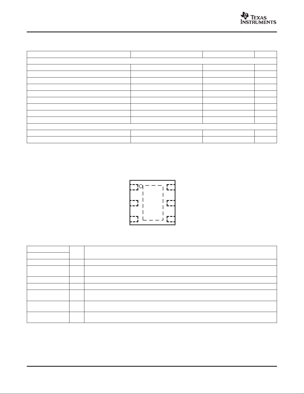
VIN
CTRL
SW
FB
COMP
GND
TOP VIEW
Thermal
Pad
6-PIN2mmx2mmx0.8mmQFN
TPS61160
TPS61161
SLVS791 – NOVEMBER 2007
ELECTRICAL CHARACTERISTICS (continued)
VIN = 3.6 V, CTRL = VIN, TA= – 40 ° C to 85 ° C, typical values are at TA= 25 ° C (unless otherwise noted)
PARAMETER TEST CONDITIONS MIN TYP MAX UNIT
EasyScale TIMING
t
start
t
EOS
t
H_LB
t
L_LB
t
H_HB
t
L_HB
V
ACKNL
t
valACKN
t
ACKN
THERMAL SHUTDOWN
T
shutdown
T
hysteresis
(2) Acknowledge condition active 0, this condition will only be applied in case the RFA bit is set. Open drain output, line needs to be pulled
high by the host with resistor load.
Start time of program stream 2 µ s
End time of program stream 2 360 µ s
High time low bit Logic 0 2 180 µ s
Low time low bit Logic 0 2 × t
High time high bit Logic 1 2 × t
H_LB
L_HB
360 µ s
360 µ s
Low time high bit Logic 1 2 180 µ s
Acknowledge output voltage low Open drain, Rpullup =15 k Ω to VIN 0.4 V
Acknowledge valid time See
Duration of acknowledge condition See
(2)
(2)
512 µ s
Thermal shutdown threshold 160 ° C
Thermal shutdown threshold hysteresis 15 ° C
2 µ s
DEVICE INFORMATION
TERMINAL FUNCTIONS
TERMINAL
NAME NO.
VIN 6 I The input supply pin for the IC. Connect VIN to a supply voltage between 2.7V and 18V.
SW 4 I
GND 3 O Ground
FB 1 I Feedback pin for current. Connect the sense resistor from FB to GND.
COMP 2 O
CTRL 5 I
Thermal Pad
I/O DESCRIPTION
This is the switching node of the IC. Connect the inductor between the VIN and SW pin. This pin is also
used to sense the output voltage for open LED protection
Output of the transconductance error amplifier. Connect an external capacitor to this pin to compensate the
regulator.
Control pin of the boost regulator. It is a multi-functional pin which can be used for enable control, PWM
and digital dimming.
The thermal pad should be soldered to the analog ground plane. If possible, use thermal via to connect to
ground plane for ideal power dissipation.
4 Submit Documentation Feedback Copyright © 2007, Texas Instruments Incorporated
Product Folder Link(s): TPS61160 TPS61161
www.ti.com
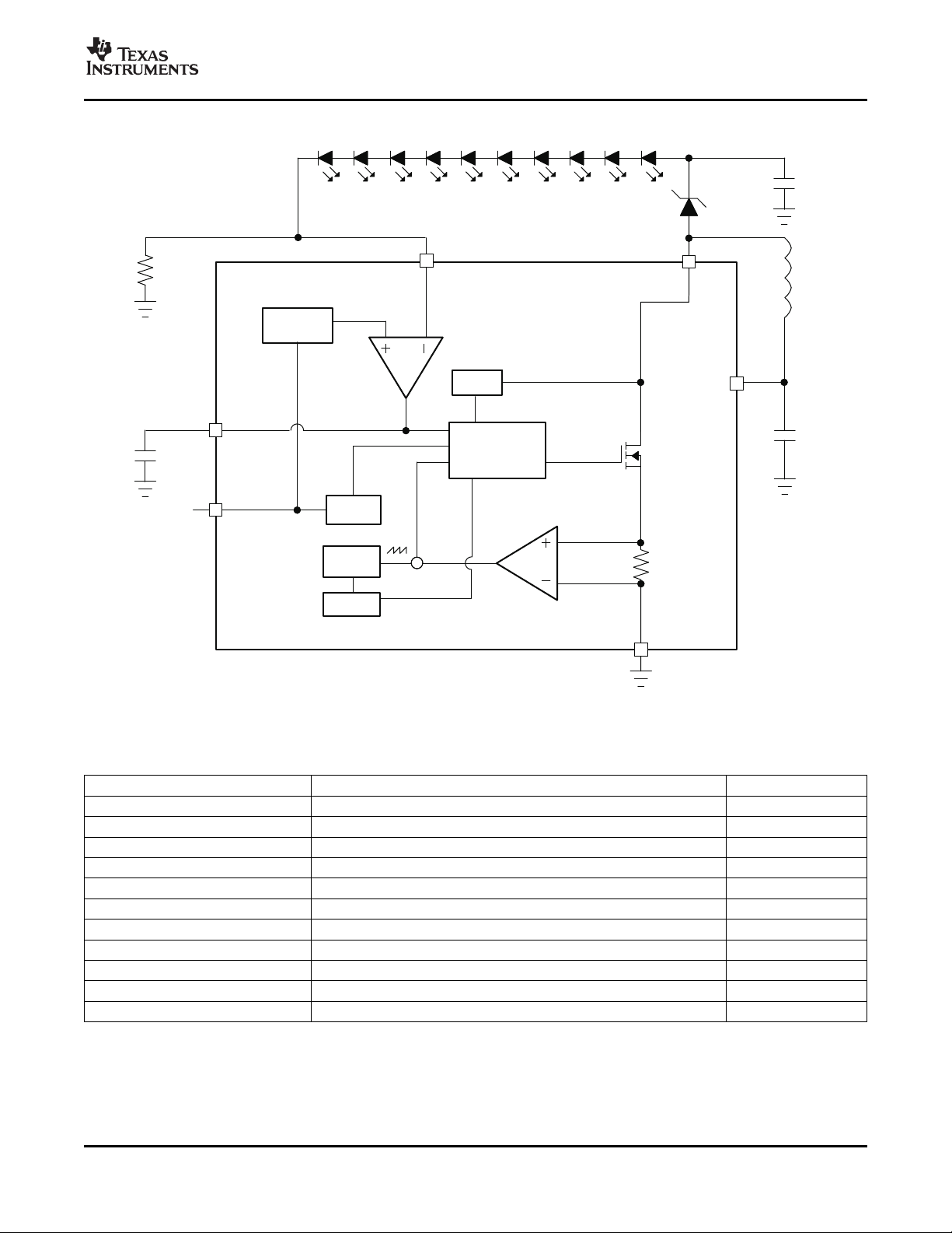
FUNCTIONAL BLOCK DIAGRAM
SW
Ramp
Generator
Oscillator
Current
Sensor
OLP
CTRL
GND
C3
L1
+
FB
Reference
Control
D1
Error
Amplifer
2
1
Rset
C2
Vin
C1
PWMControl
4
6
Soft
Start-up
5
3
COMP
TPS61160
TPS61161
SLVS791 – NOVEMBER 2007
TYPICAL CHARACTERISTICS
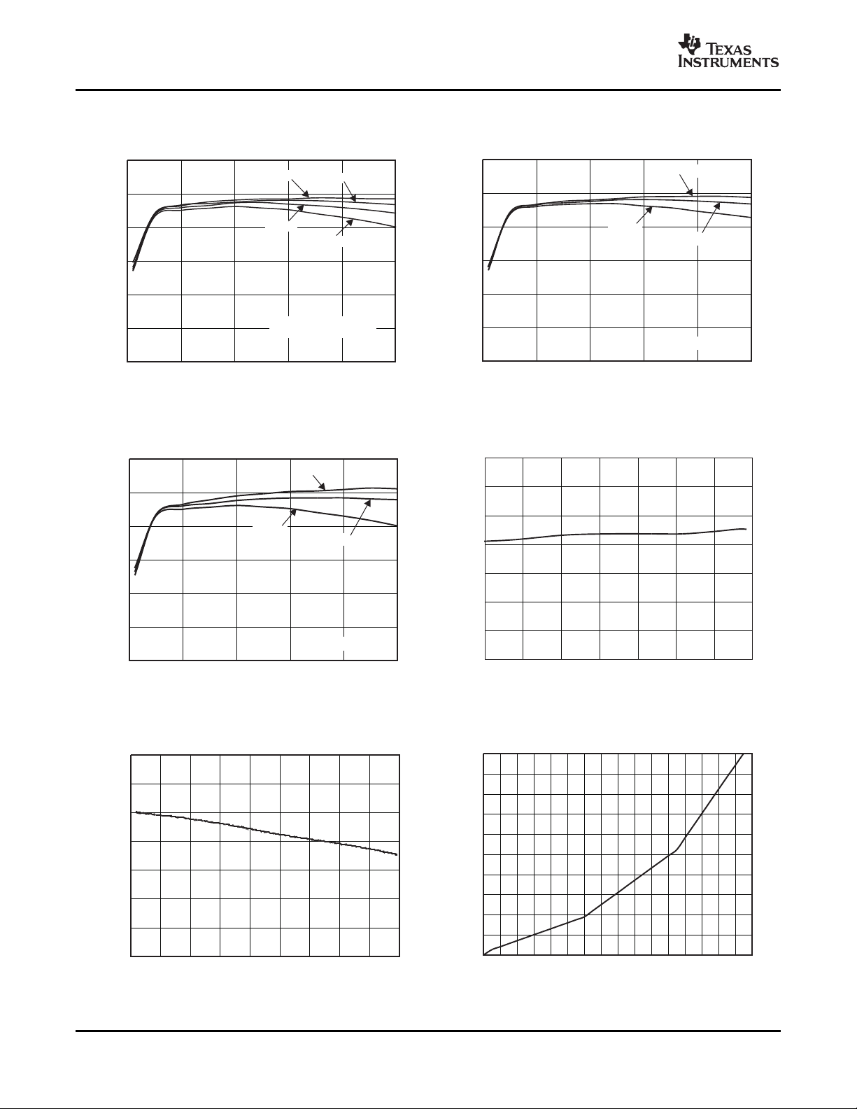
TABLE OF GRAPHS
Efficiency TPS61160/1 VIN = 3.6 V; 4, 6, 8, 10 LEDs; L = 22 µ H Figure 2
Efficiency TPS61160 Figure 3
Efficiency TPS61161 Figure 4
= 20 mA; PWM Freq = 10 kHz Figure 9
LOAD
= 20 mA; L = 22 µ H Figure 10
LOAD
Product Folder Link(s): TPS61160 TPS61161
= 20 mA; L =22 µ H Figure 11
LOAD
= 20 mA; L = 22 µ H Figure 12
LOAD
Current limit TA= 25 ° C Figure 5
Current limit Figure 6
Easyscale step Figure 7
PWM dimming linearity VIN = 3.6 V; PWM Freq = 10 kHz and 40 kHz Figure 7
Output ripple at PWM dimming 8 LEDs; VIN = 3.6 V; I
Switching waveform 8 LEDs; VIN = 3.6 V; I
Start-up 8 LEDs; VIN = 3.6 V; I
Open LED protection 8 LEDs; VIN = 3.6 V; I
Copyright © 2007, Texas Instruments Incorporated Submit Documentation Feedback 5
FIGURE
www.ti.com
40
50
60
70
80
90
100
0 10 20 30 40 50
6LEDs- TPS61160
V =3.6V
I
V =3V
I
V =4.2V
I
OutputCurrent-mA
Efficiency-%
40
50
60
70
80
90
100
0 10 20 30 40 50
OutputCurrent-mA
4(12.8V),6(19.2V)LEDs
8(25.6V),10(32V)LEDs
6LEDs
V =3.6V
I
4LEDs
8LEDs
10LEDs
Efficiency-%
300
400
500
600
700
800
900
1000
20 30 40 50 60 70 80 90
DutyCycle-%
SwitchCurrentLimit-mA
40
50
60
70
80
90
100
0 10 20 30 40 50
10LEDs- TPS61161
V =5V
I
V =3.6V
I
V =12V
I
OutputCurrent-mA
Efficiency-%
300
400
500
600
700
800
900
1000
-40 -20 0 20 40 60 80 100 120 140
Temperature- C°
SwitchCurrentLimit-mA
0
20
40
60
80
100
120
140
160
180
200
0 2 4 6 8 10 12 14 16 18 20 22 24 26 28 30 32
EasyScaleStepStep
FBVoltage-mV
TPS61160
TPS61161
SLVS791 – NOVEMBER 2007
EFFICIENCY EFFICIENCY
vs vs
OUTPUT CURRENT OUTPUT CURRENT
Figure 2. Figure 3.
EFFICIENCY SWITCH CURRENT LIMIT
vs vs
OUTPUT CURRENT DUTY CYCLE
Figure 4. Figure 5.
SWITCH CURRENT LIMIT FB VOLTAGE
TEMPERATURE EASYSCALE STEP
6 Submit Documentation Feedback Copyright © 2007, Texas Instruments Incorporated
Figure 6. Figure 7.
vs vs
Product Folder Link(s): TPS61160 TPS61161
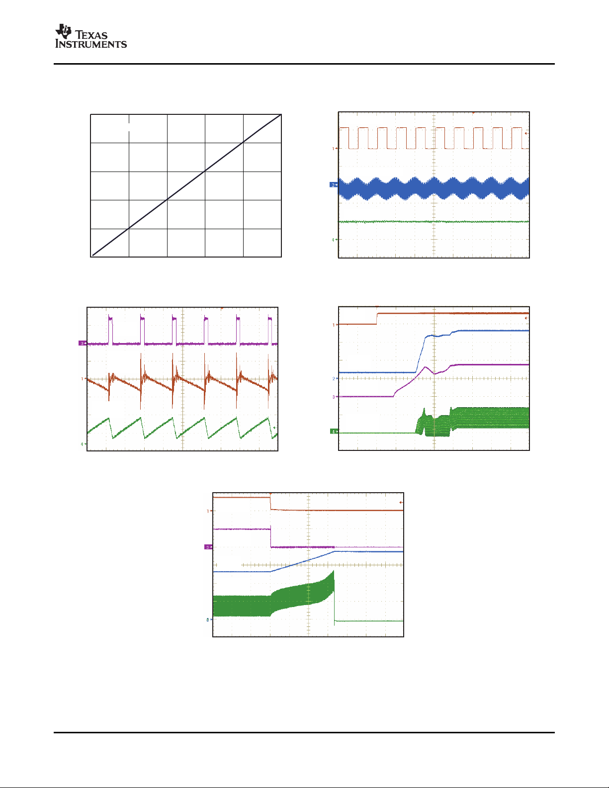
www.ti.com
t-100 s/divm
PWM2V/div
VOUT 20mV/div AC
I 10mA/div
LED
0
40
80
120
160
200
0 20 40 60 80 100
PWMDutyCycle-%
10kHz,40kHz
FBVoltage-mV
t-2ms/div
CTRL
5V/div
VOUT
10V/div
COMP
500mV/div
I
200mA/div
L
t-1 s/divm
SW
20V/div
VOUT
20mV/div
AC
I
200mA/div
L
t-100 s/divm
OPENLED
5V/div
FB
200mV/div
VOUT
10V/div
I
200mA/div
L
FB VOLTAGE
vs
PWM DUTY CYCLE OUTPUT RIPPLE at PWM DIMMING
Figure 8. Figure 9.
SWITCHING WAVEFORM START-UP
TPS61160
TPS61161
SLVS791 – NOVEMBER 2007
Figure 10. Figure 11.
Copyright © 2007, Texas Instruments Incorporated Submit Documentation Feedback 7
OPEN LED PROTECTION
Figure 12.
Product Folder Link(s): TPS61160 TPS61161

www.ti.com
I
LED
+
V
FB
R
SET
TPS61160
TPS61161
SLVS791 – NOVEMBER 2007
DETAILED DESCRIPTION
OPERATION
The TPS61160/1 is a high efficiency, high output voltage boost converter in small package size, The device is
ideal for driving up to 10 white LED in series. The serial LED connection provides even illumination by sourcing
the same output current through all LEDs, eliminating the need for expensive factory calibration. The device
integrates 40V/0.7A switch FET and operates in pulse width modulation (PWM) with 600kHz fixed switching
frequency. For operation see the block diagram. The duty cycle of the converter is set by the error amplifier
output and the current signal applied to the PWM control comparator. The control architecture is based on
traditional current-mode control; therefore, a slope compensation is added to the current signal to allow stable
operation for duty cycles larger than 50%. The feedback loop regulates the FB pin to a low reference voltage
(200mV typical), reducing the power dissipation in the current sense resistor.
SOFT START-UP
Soft-start circuitry is integrated into the IC to avoid a high inrush current during start-up. After the device is
enabled, the voltage at FB pin ramps up to the reference voltage in 32 steps, each step takes 213 µ s. This
ensures that the output voltage rises slowly to reduce the input current. Additionally, for the first 5msec after the
COMP voltage ramps, the current limit of the switch is set to half of the normal current limit spec. During this
period, the input current is kept below 400mA (typical). See the start-up waveform of a typical example,
Figure 11 .
OPEN LED PROTECTION
Open LED protection circuitry prevents IC damage as the result of white LED disconnection. The TPS61160/1
monitors the voltage at the SW pin and FB pin during each switching cycle. The circuitry turns off the switch FET
and shuts down the IC as soon as the SW voltage exceeds the Vovp threshold and the FB voltage is less than
half of regulation voltage for 8 clock cycles. As a result, the output voltage falls to the level of the input supply.
The device remains in shutdown mode until it is enabled by toggling the CTRL pin logic. To allow the use of
inexpensive low-voltage output capacitor, the TPS61160/1 has different open lamp protection thresholds to
prevent the internal 40V FET from breaking down. The threshold is set at 26V for the TPS61160 and 38V for the
TPS61161. The devices can be selected according to the number of external LEDs and their maximum forward
voltage.
SHUTDOWN
The TPS61160/1 enters shutdown mode when the CTRL voltage is logic low for more than 2.5ms. During
shutdown, the input supply current for the device is less than 1 µ A (max). Although the internal FET does not
switch in shutdown, there is still a DC current path between the input and the LEDs through the inductor and
Schottky diode. The minimum forward voltage of the LED array must exceed the maximum input voltage to
ensure that the LEDs remain off in shutdown. However, in the typical application with two or more LEDs, the
forward voltage is large enough to reverse bias the Schottky and keep leakage current low.
CURRENT PROGRAM
The FB voltage is regulated by a low 0.2V reference voltage. The LED current is programmed externally using a
current-sense resistor in series with the LED string. The value of the RSET is calculated using Equation 1 :
Where
I
= output current of LEDs
LED
V
= regulated voltage of FB
FB
R
= current sense resistor
SET
The output current tolerance depends on the FB accuracy and the current sensor resistor accuracy.
(1)
8 Submit Documentation Feedback Copyright © 2007, Texas Instruments Incorporated
Product Folder Link(s): TPS61160 TPS61161
 Loading...