Texas Instruments TPS61006DGST, TPS61006DGSR, TPS61006DGS, TPS61005DGST, TPS61002DGS Datasheet
...
TPS61000, TPS61001, TPS61002, TPS61003, TPS61004, TPS61005, TPS61006
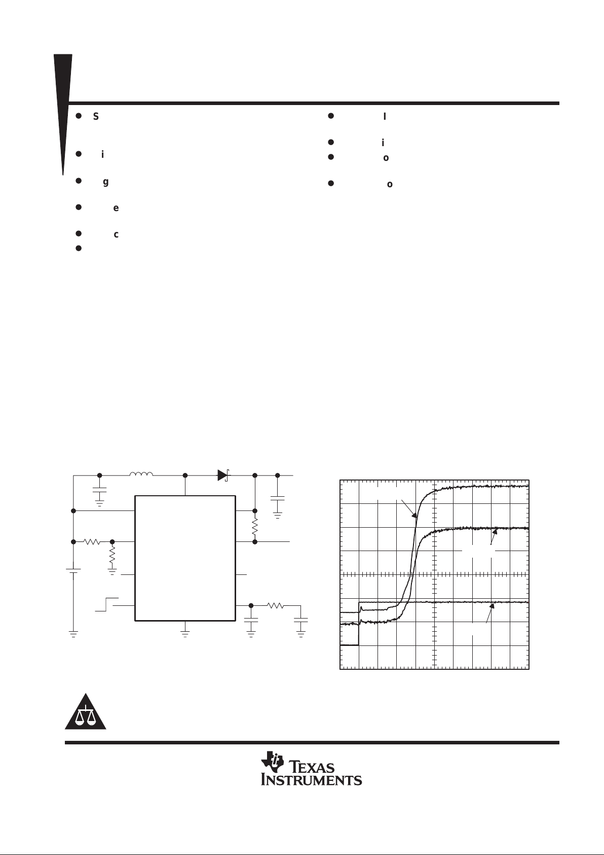
SINGLE-CELL BOOST CONVERTER WITH START-UP INTO FULL LOAD
SLVS279A – MARCH 2000 – REVISED MAY 2000
1
POST OFFICE BOX 655303 • DALLAS, TEXAS 75265
D
Start Up Into a Full Load With Supply
Voltages as Low as 0.9 V Over Full
T emperature Range
D
Minimum 100-mA Output Current From
0.8 V Supply Voltage
D
High Power Conversion Efficiency,
up to 90%
D
Power-Save Mode for Improved Efficiency
at Low Output Currents
D
Device Quiescent Current Less Than 50 µA
D
Added System Security With Integrated
Low-Battery Comparator
D
Low-EMI Converter (Integrated Antiringing
Switch Across Inductor)
D
Micro-Size 10-Pin MSOP Package
D
Evaluation Modules Available
(TPS6100xEVM–156)
D
Applications Include:
– Single- and Dual-Cell Battery Operated
Products
– MP3-Players and Wireless Headsets
– Pagers and Cordless Phones
– Portable Medical Diagnostic Equipment
– Remote Controls
·
description
The TPS6100x devices are boost converters intended for systems that are typically operated from a single- or
dual-cell nickel-cadmium (NiCd), nickel-metal hydride (NiMH), or alkaline battery . The converter output voltage
can be adjusted from 1.5 V to a maximum of 3.3 V and provides a minimum output current of 100 mA. The
converter starts up into a full load with a supply voltage of 0.9 V and stays in operation with supply voltages as
low as 0.8 V.
The converter is based on a fixed-frequency , current-mode pulse-width-modulation (PWM) controller that goes
into power-save mode at low load currents. The current through the switch is limited to a maximum of 1 100 mA,
depending on the output voltage. The current sense is integrated to further minimize external component count.
The converter can be disabled to minimize battery drain when the system is put into standby.
A low-EMI mode is implemented to reduce interference and radiated electromagnetic energy that is caused by
the ringing of the inductor when the inductor discharge-current decreases to zero. The device is packaged in
the space saving 10-pin MSOP package.
5
6
TPS61006
9
8
1
10
3
2
7
4
SW
V
BAT
LBI
NC
EN
V
OUT
LBO
FB
COMP
GND
Low Battery
Warning
R4
10 kΩ
R3
ON
OFF
R2
R1
C
i
10 µF
L1
D1
VO = 3.3 V
C1
100 pF
C2
33 nF
C
o
22 µF
33 µH
2
024681012
3
TPS61006
START UP TIMING INTO 33 Ω LOAD
14 16 18 20
1
0
– Output Voltage – V
V
O
V
OUT
EN
I
OUT
80
60
20
100
120
140
0
40
– Output Current – mA
I
O
time – ms
TYPICAL APPLICATION CIRCUIT FOR FIXED
OUTPUT VOLTAGE OPTION
Copyright 2000, Texas Instruments Incorporated
Please be aware that an important notice concerning availability, standard warranty, and use in critical applications of
Texas Instruments semiconductor products and disclaimers thereto appears at the end of this data sheet.
PRODUCTION DATA information is current as of publication date.
Products conform to specifications per the terms of Texas Instruments
standard warranty. Production processing does not necessarily include
testing of all parameters.
TPS61000, TPS61001, TPS61002, TPS61003, TPS61004, TPS61005, TPS61006
SINGLE-CELL BOOST CONVERTER WITH START-UP INTO FULL LOAD
SLVS279A – MARCH 2000 – REVISED MAY 2000
2
POST OFFICE BOX 655303 • DALLAS, TEXAS 75265
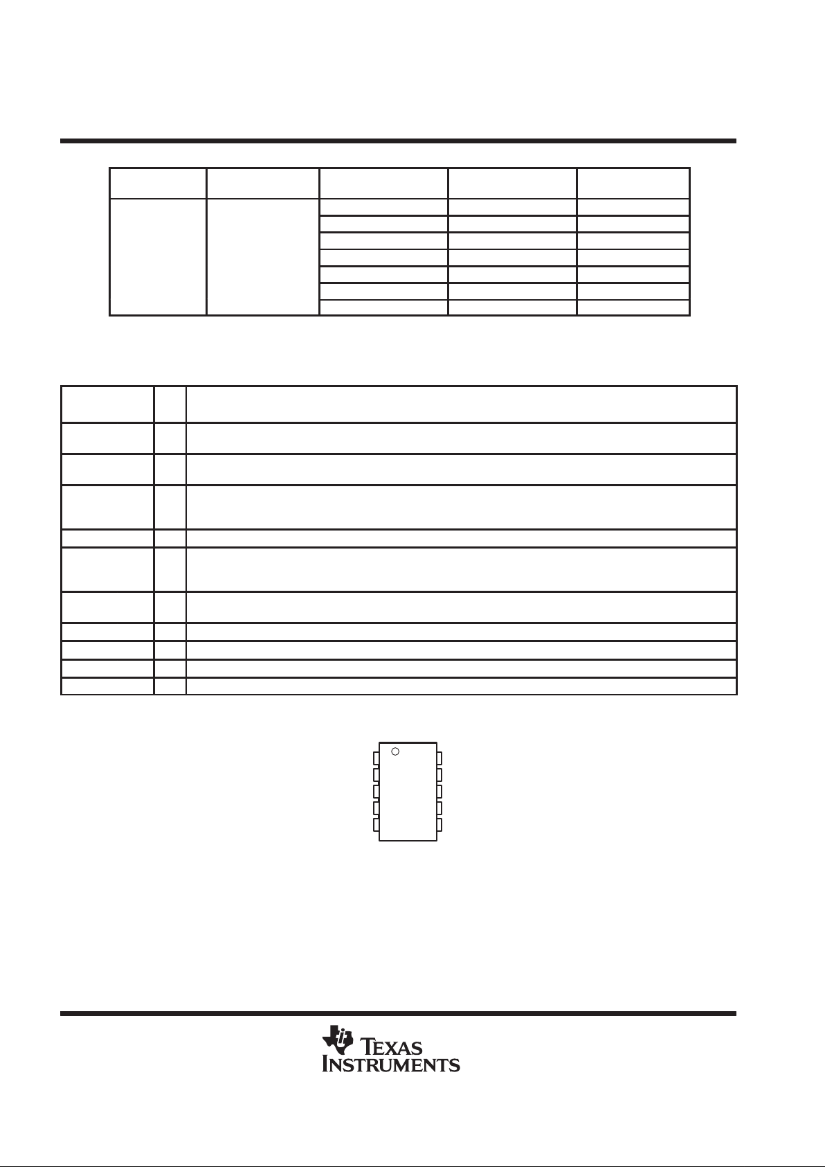
AVAILABLE OPTIONS
T
A
PACKAGE
OUTPUT VOLTAGE
(V)
PART NUMBER
†
MARKING DGS
PACKAGE
Adj. from 1.5 V to 3.3 V TPS61000DGS ADA
1.5 TPS61001DGS ADB
1.8 TPS61002DGS ADC
–40°C to 85°C 10-Pin MSOP DGS 2.5 TPS61003DGS ADD
2.8 TPS61004DGS ADE
3.0 TPS61005DGS ADF
3.3 TPS61006DGS ADG
†
The DGS package is available taped and reeled. Add R suffix to device type (e.g. TPS61000DGSR) to order quantities of
3000 devices per reel.
Terminal Functions
TERMINAL
NAME NO.
I/O
DESCRIPTION
COMP 2
Compensation of error amplifier. Connect R-C-C network to set frequency response of control loop. See the
Application
section for more details.
EN 1 I
Chip-enable input. The converter is switched on if EN is set high and is switched off when EN is connected to ground
(shutdown mode).
FB 3 I
Feedback input for adjustable output voltage (TPS61000 only). The output voltage is programmed depending on the
values of resistors R1 and R2. For the fixed output voltage versions (TPS61001, 2, 3, 4, 5, 6), leave the FB pin
unconnected.
GND 4 Ground
LBI 9 I
Low-battery detector input. A low-battery signal is generated at the LBO pin when the voltage on LBI drops below the
threshold of 500 mV . Connect LBI to GND or V
BAT
if the low-battery detector function is not used. Do not leave this
pin floating.
LBO 10 O
Open-drain low-battery detector output. This pin is pulled low if the voltage on LBI drops below the threshold of
500 mV. A pull-up resistor should be connected between LBO and V
OUT
.
NC 8 Not connected
SW 7 I Switch input pin. The node between inductor and anode of the rectifier diode is connected to this pin.
V
BAT
6 I Supply pin
V
OUT
5 O Output voltage. For the fixed output voltage versions, the integrated resistive divider is connected to this pin.
1
2
3
4
5
10
9
8
7
6
EN
COMP
FB
GND
V
OUT
LBO
LBI
NC
SW
V
BAT
DGS PACKAGE
(TOP VIEW)
TPS61000, TPS61001, TPS61002, TPS61003, TPS61004, TPS61005, TPS61006
SINGLE-CELL BOOST CONVERTER WITH START-UP INTO FULL LOAD
SLVS279A – MARCH 2000 – REVISED MAY 2000
3
POST OFFICE BOX 655303 • DALLAS, TEXAS 75265
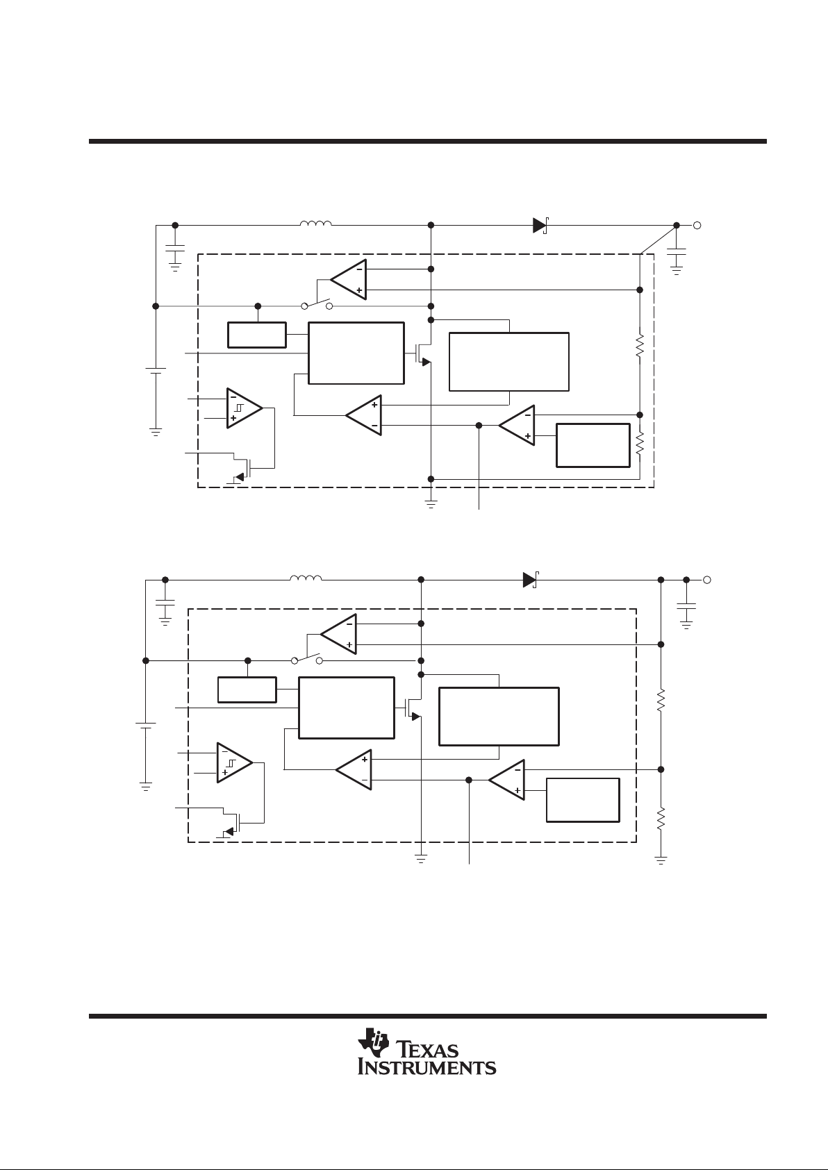
functional block diagram
fixed output-voltage option
V
REF
V
BAT
Control Logic
Oscillator
Gate Drive
UVLO
Current Sense
Current Limit
Slope Compensation
Bandgap
Reference
EN
LBI
LBO
GND COMP
L1 D1
V
OUT
C
O
C
I
SW
Comparator
LBI/LBO
Comparator
Error
Amplifier
Anti-Ringing
Comparator
and Switch
adjustable output-voltage option
V
REF
V
BAT
Control Logic
Oscillator
Gate Drive
UVLO
Current Sense
Current Limit
Slope Compensation
Bandgap
Reference
EN
LBI
LBO
GND COMP
L1 D1
V
OUT
C
O
C
I
SW
Comparator
LBI/LBO
Comparator
Error
Amplifier
Anti-Ringing
Comparator
and Switch
FB

TPS61000, TPS61001, TPS61002, TPS61003, TPS61004, TPS61005, TPS61006
SINGLE-CELL BOOST CONVERTER WITH START-UP INTO FULL LOAD
SLVS279A – MARCH 2000 – REVISED MAY 2000
4
POST OFFICE BOX 655303 • DALLAS, TEXAS 75265
detailed description
controller circuit
The device is based on a current-mode control topology using a constant-frequency pulse-width modulator to
regulate the output voltage. It runs at an oscillator frequency of 500 kHz. The current sense is implemented by
measuring the voltage across the switch. The controller also limits the current through the power switch on a
pulse by pulse basis. Care must be taken that the inductor saturation current is higher than the current limit of
the TPS6100x. This prevents the inductor from going into saturation and therefore protects both device and
inductor. The current limit should not become active during normal operating conditions.
The TPS6100x is designed for high efficiency over a wide output current range. Even at light loads the efficiency
stays high because the controller enters a power-save
mode, minimizing switching losses of the converter. In
this mode, the controller only switches if the output voltage trips below a set threshold voltage. It ramps up the
output voltage with one or several pulses, and again goes into the power-save mode once the output voltage
exceeds the threshold voltage. The controller enters the power-save mode when the output current drops to
levels that force the discontinuous current mode. It calculates a minimum duty cycle based on input and output
voltage and uses the calculation for the transition out of the
power-save mode into continuous current mode.
The control loop must be externally compensated with an R/C/C network connected to the COMP pin. See the
application section for more details on the design of the compensation network.
device enable
The device is put into operation when EN is set high. During start-up of the converter the input current from the
battery is limited until the voltage on COMP reaches its operating point. The device is put into a shutdown mode
when EN is set to GND. In this mode, the regulator stops switching and all internal control circuitry including
the low-battery comparator is switched off. The output voltage drops to one diode drop below the input voltage
in shutdown.
under-voltage lockout
An under-voltage lockout function prevents the device start-up if the supply voltage on V
BAT
is lower than
approximately 0.7 V . This under-voltage lockout function is implemented in order to prevent the malfunctioning
of the converter. When in operation and the battery is being discharged, the device will automatically enter the
shutdown mode if the voltage on V
BAT
drops below approximately 0.7 V.
If the EN pin is hardwired to V
BAT
and if the voltage at V
BAT
drops temporarily below the UVLO threshold voltage,
the device will switch off and will not start up again automatically , even if the supply voltage rises above 0.9 V.
The device will start up again only after a signal change from low to high on EN or if the battery voltage is
completely removed.

TPS61000, TPS61001, TPS61002, TPS61003, TPS61004, TPS61005, TPS61006
SINGLE-CELL BOOST CONVERTER WITH START-UP INTO FULL LOAD
SLVS279A – MARCH 2000 – REVISED MAY 2000
5
POST OFFICE BOX 655303 • DALLAS, TEXAS 75265
detailed description (continued)
low Battery detector circuit (LBI and LBO)
The low-battery detector circuit is typically used to supervise the battery voltage and to generate an error flag
when the battery voltage drops below a user-set threshold voltage. The function is active only when the device
is enabled. When the device is disabled, the LBO pin is high impedance. The LBO pin goes active low when
the voltage on the LBI pin decreases below the set threshold voltage of 500 mV ±15 mV , which is equal to the
internal reference voltage. The battery voltage, at which the detection circuit switches, can be programmed with
a resistive divider connected to the LBI pin. The resistive divider scales down the battery voltage to a voltage
level of 500 mV, which is then compared to the LBI threshold voltage. The LBI pin has a build-in hysteresis of
10 mV. Please see the application section for more details about the programming of the LBI threshold.
If the low-battery detection circuit is not used, the LBI pin should be connected to GND (or to V
BAT
) and the LBO
pin can be left unconnected. Do not let the LBI pin float.
low-EMI switch
The device integrates a circuit which removes the ringing that typically appears on the SW-node when the converter enters the discontinuous current mode. In this case, the current through the inductor ramps to zero and
the Schottky diode stops conducting. Due to remaining energy that is stored in parasitic components of diode,
inductor and switch, a ringing on the SW pin is induced. The integrated anti-ringing switch clamps this voltage
internally to V
BAT
and therefore dampens this ringing.
The anti-ringing switch is turned on by a comparator that monitors the voltage between SW and V
OUT
. This
voltage indicates when the diode is reverse biased. The ringing on the SW-node is damped to a large degree,
reducing the electromagnetic interference generated by the switching regulator to a very great extends.
adjustable output voltage
The accuracy of the internal voltage reference, the controller topology , and the accuracy of the external resistor
divider determine the accuracy of the adjustable output voltage version of the TPS61000. The reference voltage
has an accuracy of ±4% over line, load, and temperature. The controller switches between fixed frequency and
pulse-skip mode, depending on load current. This adds an offset to the output voltage that is equivalent to 1%
of VO. Using 1% accurate resistors for the feedback divider, a total accuracy of ±6% can be achieved over the
complete output current range.
TPS61000, TPS61001, TPS61002, TPS61003, TPS61004, TPS61005, TPS61006
SINGLE-CELL BOOST CONVERTER WITH START-UP INTO FULL LOAD
SLVS279A – MARCH 2000 – REVISED MAY 2000
6
POST OFFICE BOX 655303 • DALLAS, TEXAS 75265
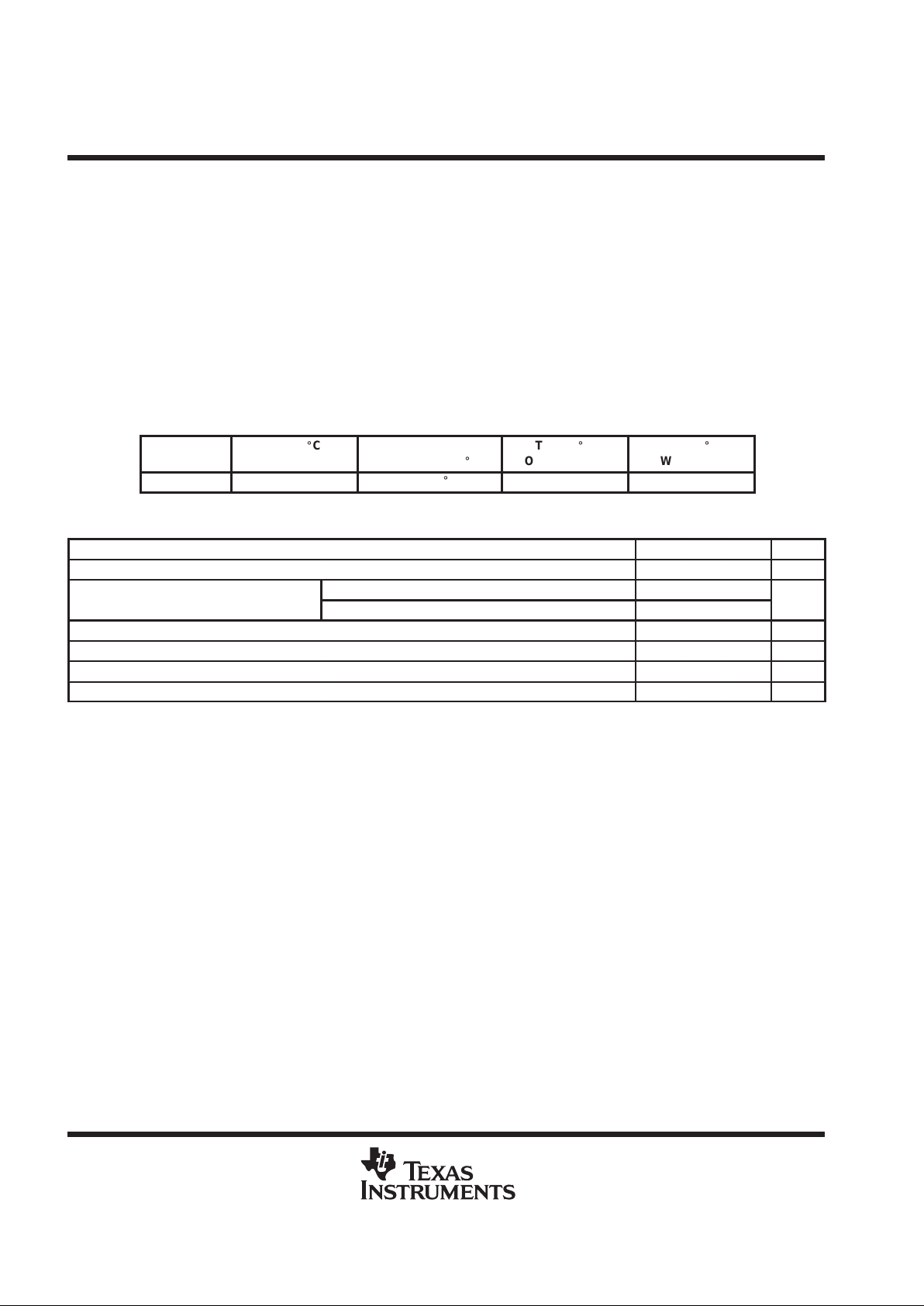
absolute maximum ratings
†
Input voltage range, VI (V
BAT
, V
OUT
, COMP, FB, LBO, EN, LBI) –0.3 V to 3.6 V. . . . . . . . . . . . . . . . . . . . . . . . .
Input voltage, VI (SW) –0.3 V to 7 V. . . . . . . . . . . . . . . . . . . . . . . . . . . . . . . . . . . . . . . . . . . . . . . . . . . . . . . . . . . . . .
Peak current into SW 1300 mA. . . . . . . . . . . . . . . . . . . . . . . . . . . . . . . . . . . . . . . . . . . . . . . . . . . . . . . . . . . . . . . . . . .
Continuous total power dissipation See dissipation rating table. . . . . . . . . . . . . . . . . . . . . . . . . . . . . . . . . . . . . . . .
Operating free-air temperature range, T
A
–40°C to 85°C. . . . . . . . . . . . . . . . . . . . . . . . . . . . . . . . . . . . . . . . . . . . .
Maximum junction temperature, T
J
150°C. . . . . . . . . . . . . . . . . . . . . . . . . . . . . . . . . . . . . . . . . . . . . . . . . . . . . . . . .
Storage temperature range, T
stg
–65°C to 150°C. . . . . . . . . . . . . . . . . . . . . . . . . . . . . . . . . . . . . . . . . . . . . . . . . . . .
Lead temperature 260°C. . . . . . . . . . . . . . . . . . . . . . . . . . . . . . . . . . . . . . . . . . . . . . . . . . . . . . . . . . . . . . . . . . . . . . . .
†
Stresses beyond those listed under “absolute maximum ratings” may cause permanent damage to the device. These are stress ratings only, and
functional operation of the device at these or any other conditions beyond those indicated under “recommended operating conditions” is not
implied. Exposure to absolute-maximum-rated conditions for extended periods may affect device reliability.
DISSIPATION RATING TABLE
PACKAGE
TA ≤ 25_C
POWER RATING
DERATING FACTOR
ABOVE TA = 25_C
TA = 70_C
POWER RATING
TA = 85_C
POWER RATING
DGS 424 mW 3.4 mW/_C 271 mW 220 mW
recommended operating conditions
MIN NOM MAX UNIT
Supply voltage at V
BAT
0.8 V
O
V
p
V
BAT
= 1.2 V 100
Output current
V
BAT
= 2.4 V 250
mA
Inductor 10 33 µH
Input capacitor 10 µF
Output capacitor 22 µF
Operating junction temperature, T
J
–40 125 °C
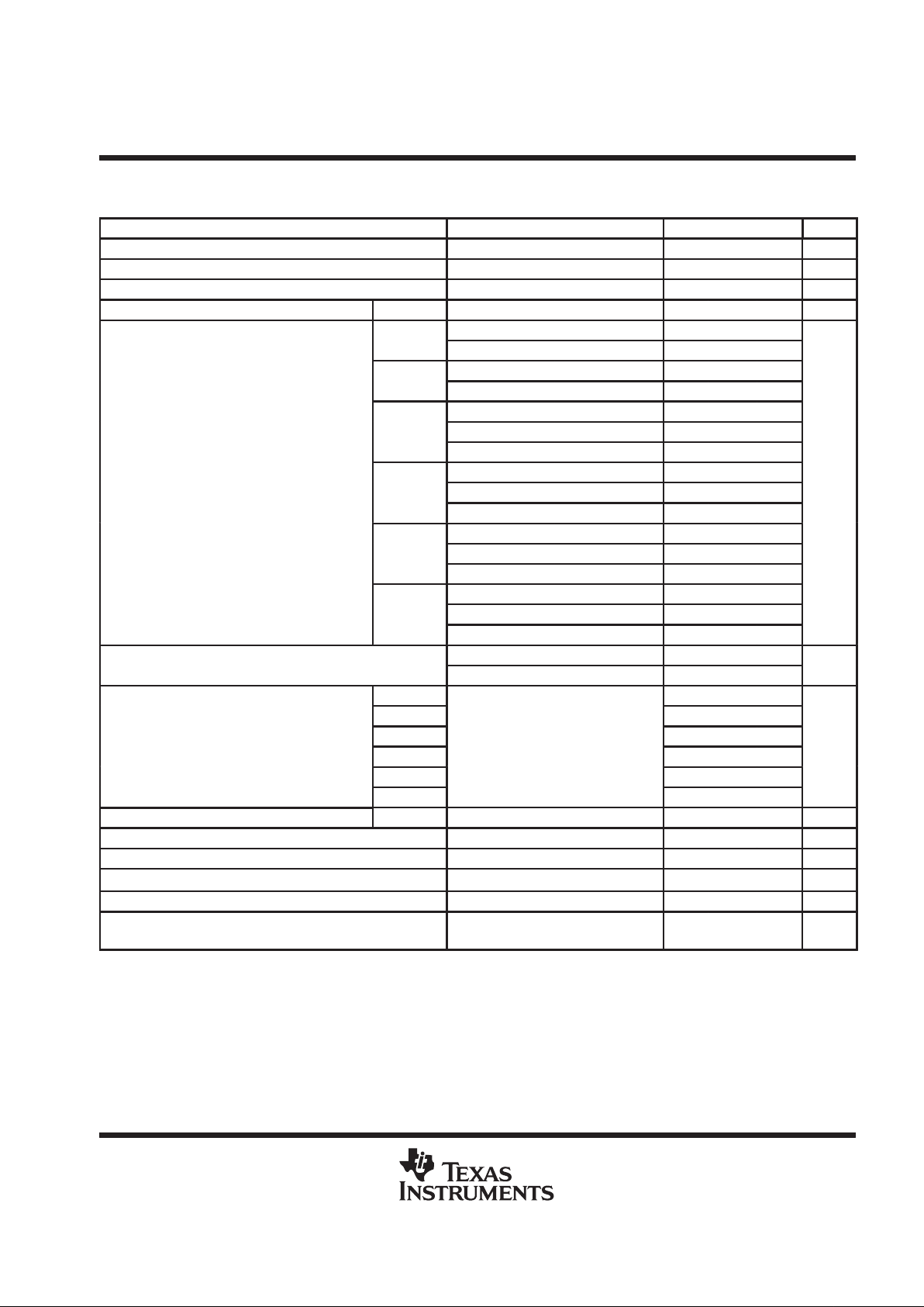
TPS61000, TPS61001, TPS61002, TPS61003, TPS61004, TPS61005, TPS61006
SINGLE-CELL BOOST CONVERTER WITH START-UP INTO FULL LOAD
SLVS279A – MARCH 2000 – REVISED MAY 2000
7
POST OFFICE BOX 655303 • DALLAS, TEXAS 75265
electrical characteristics over recommended operating free-air temperature range, V
BA T
= 1.2 V , EN
= V
BAT
(unless otherwise noted)
PARAMETER TEST CONDITIONS MIN TYP MAX UNIT
V
I
Input voltage for start-up RL = 33 Ω 0.9 V
V
I
Input voltage for start-up RL = 3 kΩ, TA = 25 °C 0.8 V
V
I
Input voltage once started IO = 100 mA 0.8 V
V
O
Programmable output voltage range TPS61000 IO = 100 mA 1.5 3.3 V
1.2 V IO = 1 mA 1.44 1.5 1.55
TPS61001
0.8 V < VI < VO, IO = 100 mA 1.45 1.5 1.55
1.2 V IO = 1 mA 1.72 1.8 1.86
TPS61002
0.8 V < VI < VO, IO = 100 mA 1.74 1.8 1.86
1.2 V IO = 1 mA 2.40 2.5 2.58
TPS61003
0.8 V < VI < VO, IO = 100 mA 2.42 2.5 2.58
1.6 V < VI < VO, IO = 200 mA 2.42 2.5 2.58
p
1.2 V IO = 1 mA 2.68 2.8 2.89
VOOutput voltage
TPS61004
0.8 V < VI < VO, IO = 100 mA 2.72 2.8 2.89
V
1.6 V < VI < VO, IO = 200 mA 2.72 2.8 2.89
1.2 V IO = 1 mA 2.88 3.0 3.1
TPS61005
0.8 V < VI < VO, IO = 100 mA 2.9 3.0 3.1
1.6 V < VI < VO, IO = 200 mA 2.9 3.0 3.1
1.2 V IO = 1 mA 3.16 3.3 3.4
TPS61006
0.8 V < VI < VO, IO = 100 mA 3.2 3.3 3.4
1.6 V < VI < VO, IO = 200 mA 3.2 3.3 3.4
p
VI = 0.8 V 100
IOMaximum continuous output current
VI = 1.8 V 250
mA
TPS61001 0.5
TPS61002 0.65
TPS61003
0.9
ISWSwitch current limit
TPS61004
0.8 V
<
V
I
<
V
O
0.95
A
TPS61005 1
TPS61006 1.1
V
FB
Feedback voltage TPS61006 468 500 515 mV
f Oscillator frequency 360 500 840 kHz
D
MAX
Maximum duty cycle 85%
r
DS(on)
Switch-on resistance VO = 3.3 V 0.18 0.27 Ω
Line regulation (see Note 1) VI = 0.8V to 1.25V , IO = 50 mA 0.3 %/V
Load regulation fixed output voltage versions
(see Note 1)
VI = 1.2 V; IO = 10 mA to 90 mA 0.25%
NOTE 1: Line and load regulation is measured as a percentage deviation from the nominal value (i.e. as percentage deviation from the nominal
output voltage). For line regulation, x %/V stands for ±x% change of the nominal output voltage per 1-V change on the input/supply
voltage. For load regulation, y% stands for ±y% change of the nominal output voltage per the specified current change.
 Loading...