

Texas Instruments TPS3828-33DBVT, TPS3828-33DBVR, TPS3825-50DBVT, TPS3825-50DBVR, TPS3825-33DBVR Datasheet
...
TPS3820-xx, TPS3823-xx, TPS3824-xx, TPS3825-xx, TPS3828-xx
PROCESSOR SUPERVISORY CIRCUITS
SLVS165C – APRIL 1998 – REVISED DECEMBER 1999
features
D
Power-On Reset Generator With Fixed
Delay Time of 200 ms (TPS3823/4/5/8)
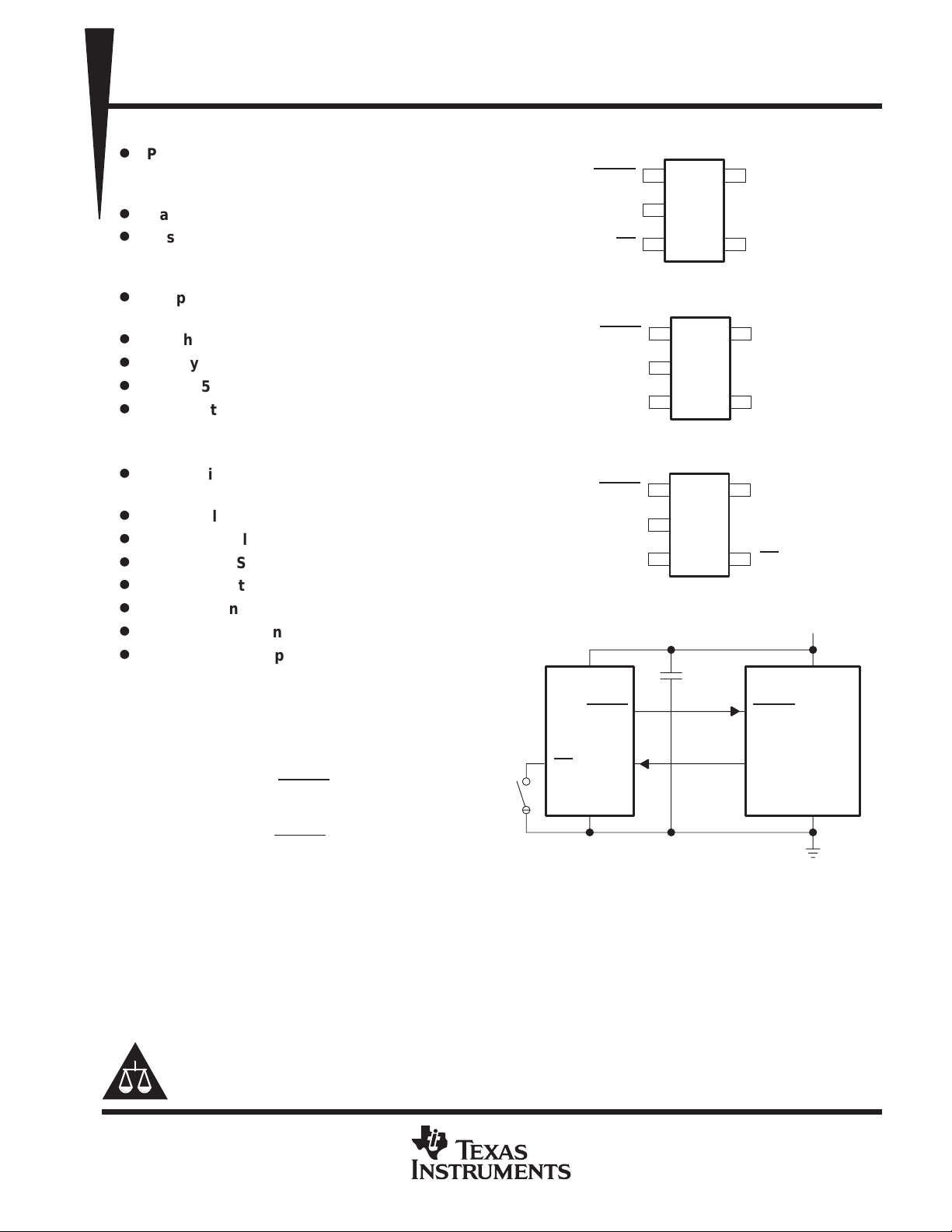
TPS3820, TPS3823, TPS3828 . . . DBV PACKAGE
(TOP VIEW)
RESET
1
V
5
DD
or 25 ms (TPS3820)
D
Manual Reset Input (TPS3820/3/5/8)
D
Reset Output Available in Active-Low
(TPS3820/3/4/5), Active-High (TPS3824) and
Open-Drain (TPS3828)
D
Supply Voltage Supervision Range
GND
MR
2
3
4
WDI
TPS3824 . . . DBV PACKAGE
(TOP VIEW)
2.5 V, 3 V, 3.3 V, 5 V
D
Watchdog Timer (TPS3820/3/4/8)
D
Supply Current of 15 µA (Typ)
D
SOT23-5 Package
D
T emperature Range ...–40°C to 85°C
applications
D
Applications Using DSPs, Microcontrollers,
or Microprocessors
D
Industrial Equipment
D
Programmable Controls
D
Automotive Systems
D
Portable/Battery-Powered Equipment
D
Intelligent Instruments
D
Wireless Communications Systems
D
Notebook/Desktop Computeres
description
The TPS382x family of supervisors provides
circuit initialization and timing supervision,
primarily for DSP and processor-based systems.
RESET
GND
RESET
TPS3825 . . . DBV PACKAGE
RESET
GND
RESET
typical application
V
DD
RESET
TPS3823-33
MR WDI
1
2
3
(TOP VIEW)
1
2
3
100 nF
V
5
4
5
4
DD
WDI
V
DD
MR
RESET
MSP430C325
I/O
During power-on, RESET is asserted when
supply voltage VDD becomes higher than 1.1 V.
GND
Thereafter, the supply voltage supervisor monitors V
remains below the threshold voltage V
and keeps RESET active as long as V
DD
DD
IT–
.
An internal timer delays the return of the output to the inactive state (high) to ensure proper system reset. The
delay time, td, starts after VDD has risen above the threshold voltage V
the threshold voltage V
, the output becomes active (low) again. No external components are required. All
IT–
the devices of this family have a fixed-sense threshold voltage V
. When the supply voltage drops below
IT–
set by an internal voltage divider.
IT–
3.3 V
V
DD
GND
Please be aware that an important notice concerning availability, standard warranty, and use in critical applications of
Texas Instruments semiconductor products and disclaimers thereto appears at the end of this data sheet.
PRODUCTION DATA information is current as of publication date.
Products conform to specifications per the terms of Texas Instruments
standard warranty. Production processing does not necessarily include
testing of all parameters.
POST OFFICE BOX 655303 • DALLAS, TEXAS 75265
Copyright 1999, Texas Instruments Incorporated
1
TPS3820-xx, TPS3823-xx, TPS3824-xx, TPS3825-xx, TPS3828-xx
PROCESSOR SUPERVISORY CIRCUITS
SLVS165C – APRIL 1998 – REVISED DECEMBER 1999
description (continued)
The TPS3820/3/5/8 devices incorporate a manual reset input, MR. A low level at MR causes RESET to become
active. The TPS3824/5 devices include a high-level output RESET . TPS3820/3/4/8 have a watchdog timer that
is periodically triggered by a positive or negative transition at WDI. When the supervising system fails to retrigger
the watchdog circuit within the time-out interval, t
also reinitializes the watchdog timer. Leaving WDI unconnected disables the watchdog.
The product spectrum is designed for supply voltages of 2.5 V, 3 V, 3.3 V, and 5 V. The circuits are available
in a 5-pin SOT23-5 package. The TPS382x devices are characterized for operation over a temperature range
of -40°C to 85°C.
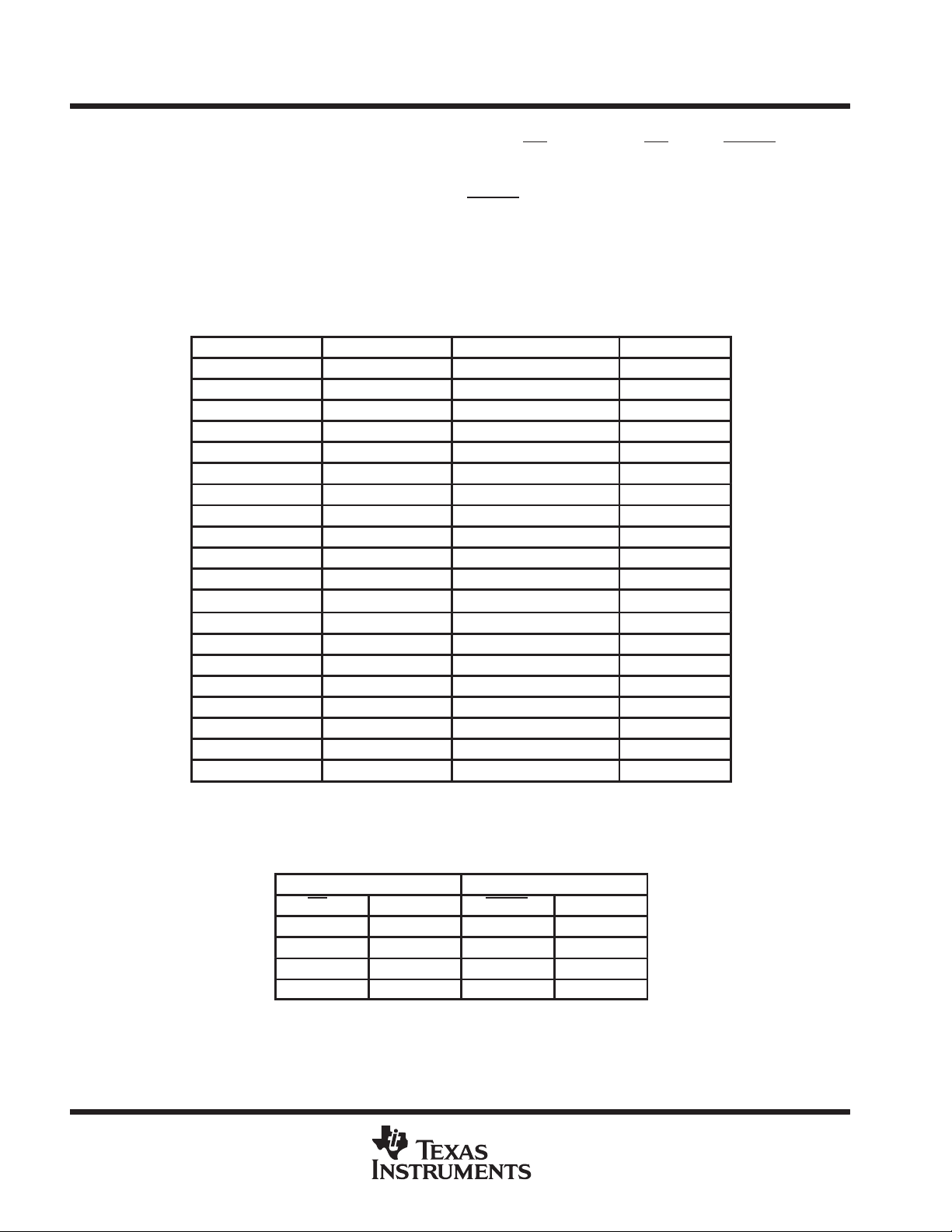
PACKAGE INFORMATION
DEVICE NAME
TPS3820-25DBVT†TPS3820-25DBVR
TPS3820-30DBVT†TPS3820-30DBVR
TPS3820-33DBVT†TPS3820-33DBVR
TPS3820-50DBVT†TPS3820-50DBVR
TPS3823-25DBVT†TPS3823-25DBVR
TPS3823-30DBVT†TPS3823-30DBVR
TPS3823-33DBVT†TPS3823-33DBVR
TPS3823-50DBVT†TPS3823-50DBVR
TPS3824-25DBVT†TPS3824-25DBVR
TPS3824-30DBVT†TPS3824-30DBVR
TPS3824-33DBVT†TPS3824-33DBVR
TPS3824-50DBVT†TPS3824-50DBVR
TPS3825-25DBVT†TPS3825-25DBVR
TPS3825-30DBVT†TPS3825-30DBVR
TPS3825-33DBVT†TPS3825-33DBVR
TPS3825-50DBVT†TPS3825-50DBVR
TPS3828-25DBVT†TPS3828-25DBVR
TPS3828-30DBVT†TPS3828-30DBVR
TPS3828-33DBVT†TPS3828-33DBVR
TPS3828-50DBVT†TPS3828-50DBVR
†
The DBVT package indicates tape and reel of 250 parts.
‡
The DBVR package indicates tape and reel of 3000 parts.
§
This device is in the Product Preview stage of development. Contact the local TI sales office for
availability
DEVICE NAME THRESHOLD VOLTAGE MARKING
FUNCTION/TRUTH TABLE
, RESET becomes active for the time period td. This event
tout
‡§
‡§
‡
‡
‡
‡
‡
‡
‡
‡
‡
‡
‡§
‡§
‡
‡
‡§
‡§
‡
‡
2.25 V
2.63 V
2.93 V PDEI
4.55 V PDDI
2.25 V PAPI
2.63 V PAQI
2.93 V PARI
4.55 V PASI
2.25 V PATI
2.63 V PAUI
2.93 V PAVI
4.55 V PAWI
2.25 V
2.63 V
2.93 V PDGI
4.55 V PDFI
2.25 V
2.63 V
2.93 V PDII
4.55 V PDHI
INPUTS
‡
MR
L 0 L H
L 1 L H
H 0 L H
H 1 H L
†
TPS3824/5
‡
TPS3820/3/5/8
2
POST OFFICE BOX 655303 • DALLAS, TEXAS 75265
VDD>V
IT
OUTPUTS
RESET RESET
†
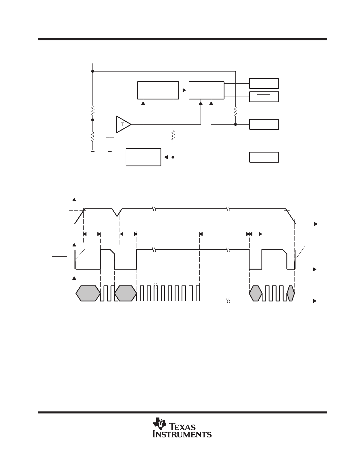
functional block diagram
V
DD
TPS3820-xx, TPS3823-xx, TPS3824-xx, TPS3825-xx, TPS3828-xx
PROCESSOR SUPERVISORY CIRCUITS
SLVS165C – APRIL 1998 – REVISED DECEMBER 1999
†
52 kΩ
Reset
Reset
MR
‡
Watchdog
Timer Logic
+
_
V
ref
40 kΩ
Reset
Logic
timing diagram
V
IT
V
DD
1.1 V
RESET
WDI
X = Don’t care
Transition
Detector
†
TPS3824/5
‡
TPS3820/3/5/8
t
d
undefined
XX XX
t
d
t
t(out)
WDI
t
d
undefined
POST OFFICE BOX 655303 • DALLAS, TEXAS 75265
3

TPS3820-xx, TPS3823-xx, TPS3824-xx, TPS3825-xx, TPS3828-xx
PROCESSOR SUPERVISORY CIRCUITS
SLVS165C – APRIL 1998 – REVISED DECEMBER 1999
absolute maximum ratings over operating free-air temperature range (unless otherwise noted)
Supply voltage, VDD (see Note 1) 6 V. . . . . . . . . . . . . . . . . . . . . . . . . . . . . . . . . . . . . . . . . . . . . . . . . . . . . . . . . . . . .
Input voltage, MR, WDI (see Note 1) –0.3 V to (VDD + 0.3 V). . . . . . . . . . . . . . . . . . . . . . . . . . . . . . . . . . . . . . . .
Maximum low output current, IOL 5 mA. . . . . . . . . . . . . . . . . . . . . . . . . . . . . . . . . . . . . . . . . . . . . . . . . . . . . . . . . . .
Maximum high output current, I
–5 mA. . . . . . . . . . . . . . . . . . . . . . . . . . . . . . . . . . . . . . . . . . . . . . . . . . . . . . . . .
OH
Input clamp current range, IIK (VI < 0 or VI > VDD) ±10 mA. . . . . . . . . . . . . . . . . . . . . . . . . . . . . . . . . . . . . . . . . .
Output clamp current range, IOK (VO < 0 or VO > VDD) ±10 mA. . . . . . . . . . . . . . . . . . . . . . . . . . . . . . . . . . . . . .
Continuous total power dissipation See Dissipation Rating Table. . . . . . . . . . . . . . . . . . . . . . . . . . . . . . . . . . . . .
Operating free-air temperature range, TA –40°C to 85°C. . . . . . . . . . . . . . . . . . . . . . . . . . . . . . . . . . . . . . . . . . . .
Storage temperature range, T
–65°C to 150°C. . . . . . . . . . . . . . . . . . . . . . . . . . . . . . . . . . . . . . . . . . . . . . . . . . .
stg
Soldering temperature 260°C. . . . . . . . . . . . . . . . . . . . . . . . . . . . . . . . . . . . . . . . . . . . . . . . . . . . . . . . . . . . . . . . . . . .
†
Stresses beyond those listed under “absolute maximum ratings” may cause permanent damage to the device. These are stress ratings only, and
functional operation of the device at these or any other conditions beyond those indicated under “recommended operating conditions” is not
implied. Exposure to absolute-maximum-rated conditions for extended periods may affect device reliability.
NOTE 1: All voltage values are with respect to GND.
DISSIPATION RATING TABLE
PACKAGE
DBV 437 mW 3.5 mW/°C 280 mW 227 mW
TA ≤ 25°C
POWER RATING
OPERATING FACTOR
ABOVE TA = 25°C
TA = 70°C
POWER RATING
TA = 85°C
POWER RATING
recommended operating conditions
MIN MAX UNIT
Supply voltage, V
Input voltage, V
High-level input voltage at MR and WDI, V
Low-level input voltage, V
Input transition rise and fall rate at MR or WDI, ∆t/∆V 100 ns/V
Operating free-air temperature range, T
DD
I
IH
IL
A
1.1 5.5 V
0 VDD + 0.3 V
0.7 × V
DD
0.3 × V
DD
–40 85 °C
V
V
†
4
POST OFFICE BOX 655303 • DALLAS, TEXAS 75265

0.8
V
RESET
0.8
V
V
RESET
DD IT
0.4
V
RESET
DD IT
0.4
V
T
0°C
85°C
V
V
ggg
T
40°C
85°C
V
V
Hysteresis at V
input
mV
TPS3820-xx, TPS3823-xx, TPS3824-xx, TPS3825-xx, TPS3828-xx
PROCESSOR SUPERVISORY CIRCUITS
SLVS165C – APRIL 1998 – REVISED DECEMBER 1999
electrical characteristics over recommended operating free-air temperature range (unless
otherwise noted)
PARAMETER TEST CONDITIONS MIN TYP MAX UNIT
TPS382x-25
RESET
V
OH
V
OL
IT–
hys
NOTES: 2. The lowest supply voltage at which RESET becomes active. tr,
High-level output voltage
Low-level output voltage
Power-up reset voltage (see Note 2) VDD ≥ 1.1 V, IOL = 20 µA 0.4 V
Negative-going input threshold
voltage (see Note 3)
p
DD
3. To ensure best stability of the threshold voltage, a bypass capacitor (ceramic, 0.1 µF) should be placed near the supply terminals.
TPS382x-30
TPS382x-33
TPS382x-50
TPS3824-25
TPS3825-25
TPS3824-30
TPS3825-30
TPS3824-33
TPS3825-33
TPS3824-50
TPS3825-50
TPS3824-25
TPS3825-25
TPS3824-30
TPS3825-30
TPS3824-33
TPS3825-33
TPS3824-50
TPS3825-50
TPS382x-25
TPS382x-30
TPS382x-33
TPS382x-50
TPS382x-25 2.21 2.25 2.30
TPS382x-30
TPS382x-33
TPS382x-50
TPS382x-25
TPS382x-30
TPS382x-33
TPS382x-50 4.46 4.55 4.64
TPS382x-25
TPS382x-30
TPS382x-33
TPS382x-50 50
VDD = V
IOH = –20 µA
VDD = V
IOH = –30 µA
VDD = V
IOH = –120 µA
VDD ≥ 1.8 V, IOH = –100 µA
VDD ≥ 1.8 V, IOH = –150 µA
VDD = V
IOL = 1 mA
V
IOL = 1.2 mA
VDD = V
IOL = 3 mA
VDD = V
IOL = 1 mA
V
IOL = 1.2 mA
VDD = V
IOL = 3 mA
=
A
= –
A
+ 0.2 V
IT–
+ 0.2 V
IT–
+ 0.2 V
IT–
+ 0.2 V
IT–
= V– + 0.2 V
+ 0.2 V
IT–
– 0.2 V
IT–
= V– –0.2 V
– 0.2 V
IT–
°
°
–
°
°
–
≥ 15 µs/V
VDD
×
DD
VDD – 1.5 V
×
DD
2.59 2.63 2.69
2.88 2.93 3
4.49 4.55 4.64
2.20 2.25 2.30
2.57 2.63 2.69
2.86 2.93 3
30
V
POST OFFICE BOX 655303 • DALLAS, TEXAS 75265
5

TPS3820-xx, TPS3823-xx, TPS3824-xx, TPS3825-xx, TPS3828-xx
WDI
µ
µ
IILLow-level input current
I
RESET
DD IT,max
,
A
t
Watchdog time out
DD IT
,
tdDelay time
DD IT
,
ms
PHL
high-to-low-level out ut
µ
µ
PLH
low-to-high-level out ut
µ
PROCESSOR SUPERVISORY CIRCUITS
SLVS165C – APRIL 1998 – REVISED DECEMBER 1999
electrical characteristics over recommended operating free-air temperature range (unless
otherwise noted) (continued)
PARAMETER TEST CONDITIONS MIN TYP MAX UNIT
I
IH(AV)
I
IL(AV)
I
IH
OS
I
DD
C
i
NOTE 4: The RESET short-circuit current is the maximum pullup current when RESET is driven low by a µP bidirectional reset pin.
Average high-level input current
Average low-level input current
WDI WDI = V
High-level input current
p
Output short-circuit current
(see Note 4)
Supply current
Internal pullup resistor at MR 52 kΩ
Input capacitance at MR, WDI VI = 0 V to 5.5 V 5 pF
MR
WDI WDI = 0.3 V, VDD = 5.5 V 140 190
MR MR = 0.3 V, VDD = 5.5 V –110 –160
TPS382x-25
TPS382x-30
TPS382x-33
TPS382x-50 –800
WDI = VDD,
time average (dc = 88%)
WDI = 0.3 V, VDD = 5.5 V
time average (dc = 12%)
DD
MR = VDD × 0.7,
VDD = 5.5 V
V
= V
+ 0.2 V,
VO = 0 V
WDI and MR unconnected,
Outputs unconnected
120
–15
140 190
–40 –60
–400
15 25 µA
A
µ
timing requirements at RL = 1 MΩ, CL = 50 pF, TA = 25°C
PARAMETER TEST CONDITIONS MIN MAX UNIT
t
w
Pulse width
at V
DD
at MR
at WDI VDD ≥ V
VDD = V
VDD ≥ V
+ 0.2 V, VDD = V
IT–
+ 0.2 V, VIL = 0.3 x VDD, VIH = 0.7 x V
IT–
+ 0.2 V, VIL = 0.3 x VDD, VIH = 0.7 x V
IT–
- 0.2 V 6 µs
IT-
switching characteristics at RL = 1 MΩ, CL = 50 pF, TA = 25°C
PARAMETER TEST CONDITIONS MIN TYP MAX UNIT
tout
Propagation (delay) time,
t
PHL
Propagation (delay) time,
t
TPS3820
TPS3823/4/8
TPS3820
TPS3823/4/5/8
MR to RESET delay
(TPS3820/3/5/8)
p
VDD to RESET delay
MR to RESET delay (TPS3824/5)
p
VDD to RESET delay (TPS3824/5)
V
≥ V– + 0.2 V,
See Timing Diagram
V
≥V– +0.2 V,
See timing diagram
VDD≥V
VIL=0.3 x VDD,
VIH=0.7 x V
VIL = V
VIH = V
VDD≥V
VIL=0.3 x VDD,
VIH=0.7 x V
VIL = V
VIH = V
+0.2 V,
IT–
- 0.2 V,
IT-
+ 0.2 V
IT-
+0.2 V,
IT–
- 0.2 V,
IT-
+ 0.2 V
IT-
DD
DD
DD
DD
112 200 310 ms
0.9 1.6 2.5 s
15 25 37
120 200 300
1 µs
100 ns
0.1
25
0.1
25
µs
s
6
POST OFFICE BOX 655303 • DALLAS, TEXAS 75265

TPS3820-xx, TPS3823-xx, TPS3824-xx, TPS3825-xx, TPS3828-xx
PROCESSOR SUPERVISORY CIRCUITS
SLVS165C – APRIL 1998 – REVISED DECEMBER 1999
TYPICAL CHARACTERISTICS
(25°C)
IT
), V
A
(T
IT
Normalized Input Threshold Voltage – V
Aµ
– Input Current –I
I
NORMALIZED INPUT THRESHOLD VOLTAGE
vs
FREE-AIR TEMPERATURE AT V
1.001
1
0.999
0.998
0.997
0.996
0.995
–40
–15 10 35
TA – Free-Air Temperature – °C
Figure 1
INPUT CURRENT
vs
INPUT VOLTAGE AT MR
50
VDD = 5.5 V
WDI = Open
0
–50
–100
–150
–40°C
85°C
DD
60 85
19
17
15
Aµ
13
11
9
7
– Supply Current –I
5
DD
3
1
–1
–0.5
3
2.5
2
1.5
1
– Low-Level Output Voltage – V
OL
0.5
V
SUPPLY CURRENT
vs
SUPPLY VOLTAGE
MR = Open
WDI = Open
TA = 25°C
TPS382x-33
0.5 1.5 2.5 3.5
VDD – Supply Voltage – V
Figure 2
LOW-LEVEL OUTPUT VOLTAGE
vs
LOW-LEVEL OUTPUT CURRENT
VDD = 2.66 V
WDI = Open
= Open
MR
85°C
4.5 6.5
5.5
–40°C
–200
–101234 65
VI – Input Voltage at MR
Figure 3
0
0
1
– V
POST OFFICE BOX 655303 • DALLAS, TEXAS 75265
2345678910
IOL – Low-Level Output Current – mA
Figure 4
7

TPS3820-xx, TPS3823-xx, TPS3824-xx, TPS3825-xx, TPS3828-xx
PROCESSOR SUPERVISORY CIRCUITS
SLVS165C – APRIL 1998 – REVISED DECEMBER 1999
TYPICAL CHARACTERISTICS
3.5
3
2.5
2
1.5
1
– High-Level Output Voltage – V
OH
V
0.5
0
0 –50
HIGH-LEVEL OUTPUT VOLTAGE
vs
HIGH-LEVEL OUTPUT CURRENT
VDD = 3.2 V
WDI = Open
= Open
MR
–40°C
85°C
–100 –150 –200 –250
IOH – High-Level Output Current – µA
Figure 5
MINIMUM PULSE DURATION AT V
V
DD
10
sµ
–
8
DD
6
5
4
3
2
– High-Level Output Voltage – V
OH
1
V
0
0
–100 –200 –300 –400
IOH – High-Level Output Current – µA
vs
THRESHOLD OVERDRIVE
WDI = Open
MR
= Open
HIGH-LEVEL OUTPUT VOLTAGE
vs
HIGH-LEVEL OUTPUT CURRENT
VDD = 5.5 V
WDI = Open
= Open
MR
–40°C
85°C
–500 –600
Figure 6
DD
–700
6
4
2
– Minimum Pulse Duration at V
w
t
0
0
200 400 600 800
VDD – Threshold Overdrive – mV
1000
Figure 7
8
POST OFFICE BOX 655303 • DALLAS, TEXAS 75265

TPS3820-xx, TPS3823-xx, TPS3824-xx, TPS3825-xx, TPS3828-xx
PROCESSOR SUPERVISORY CIRCUITS
SLVS165C – APRIL 1998 – REVISED DECEMBER 1999
MECHANICAL DATA
DBV (R-PDSO-G5) PLASTIC SMALL-OUTLINE PACKAGE
0,95
1,30
1,00
0,40
0,20
45
1,80
1,50
1
3,10
2,70
3
0,05 MIN
M
0,25
3,00
2,50
Seating Plane
0,10
0,15 NOM
0°–8°
Gage Plane
0,25
0,55
0,35
NOTES: A. All linear dimensions are in millimeters.
B. This drawing is subject to change without notice.
C. Body dimensions include mold flash or protrusion.
4073253-4/B 10/97
POST OFFICE BOX 655303 • DALLAS, TEXAS 75265
9

IMPORTANT NOTICE
T exas Instruments and its subsidiaries (TI) reserve the right to make changes to their products or to discontinue
any product or service without notice, and advise customers to obtain the latest version of relevant information
to verify, before placing orders, that information being relied on is current and complete. All products are sold
subject to the terms and conditions of sale supplied at the time of order acknowledgement, including those
pertaining to warranty, patent infringement, and limitation of liability.
TI warrants performance of its semiconductor products to the specifications applicable at the time of sale in
accordance with TI’s standard warranty. Testing and other quality control techniques are utilized to the extent
TI deems necessary to support this warranty . Specific testing of all parameters of each device is not necessarily
performed, except those mandated by government requirements.
CERTAIN APPLICATIONS USING SEMICONDUCTOR PRODUCTS MAY INVOLVE POTENTIAL RISKS OF
DEATH, PERSONAL INJURY, OR SEVERE PROPERTY OR ENVIRONMENTAL DAMAGE (“CRITICAL
APPLICATIONS”). TI SEMICONDUCTOR PRODUCTS ARE NOT DESIGNED, AUTHORIZED, OR
WARRANTED TO BE SUITABLE FOR USE IN LIFE-SUPPORT DEVICES OR SYSTEMS OR OTHER
CRITICAL APPLICA TIONS. INCLUSION OF TI PRODUCTS IN SUCH APPLICATIONS IS UNDERST OOD TO
BE FULLY AT THE CUSTOMER’S RISK.
In order to minimize risks associated with the customer’s applications, adequate design and operating
safeguards must be provided by the customer to minimize inherent or procedural hazards.
TI assumes no liability for applications assistance or customer product design. TI does not warrant or represent
that any license, either express or implied, is granted under any patent right, copyright, mask work right, or other
intellectual property right of TI covering or relating to any combination, machine, or process in which such
semiconductor products or services might be or are used. TI’s publication of information regarding any third
party’s products or services does not constitute TI’s approval, warranty or endorsement thereof.
Copyright 1999, Texas Instruments Incorporated
 Loading...