

Delay (s) = CT (nF) + 0.5 x 10⁻³ (s)
20ms Delay
300ms Delay
(c)
(b)
(a)
175
3.3V
TPS3808G33
V
DD
SENSE
CTRESET
3.3V
TPS3808G33
V
DD
SENSE
C
T
C
T
RESET
3.3V
TPS3808G33
V
DD
SENSE
C
T
50k
Ω
RESET
Product
Folder
Sample &
Buy
Technical
Documents
Tools &
Software
Support &
Community
SBVS103D –APRIL 2008–REVISED DECEMBER 2014
TPS3808-EP Low Quiescent Current, Programmable Delay Supervisory Circuit
1 Features 2 Applications
1
• Controlled Baseline
– One Assembly Site
– One Test Site
– One Fabrication Site
• Extended Temperature Performance of
–55°C to 125°C
• Enhanced Diminishing Manufacturing Sources
(DMS) Support
• Enhanced Product-Change Notification
• Qualification Pedigree
(1)
• Power-On Reset Generator With Adjustable Delay
Time: 1.25 ms to 10 s
• Very Low Quiescent Current: 2.4 μA Typical
• High Threshold Accuracy: 0.5% Typical
• Fixed Threshold Voltages for Standard Voltage
Rails From 0.9 V to 5 V and Adjustable Voltage
Down to 0.4 V Are Available
• Manual Reset (MR) Input
• Open-Drain RESET Output
• Temperature Range: –55°C to 125°C
• Small SOT-23 Package
(1) Component qualification in accordance with JEDEC and
industry standards to ensure reliable operation over an
extended temperature range. This includes, but is not limited Device Information
to, Highly Accelerated Stress Test (HAST) or biased 85/85,
temperature cycle, autoclave or unbiased HAST,
electromigration, bond intermetallic life, and mold compound
life. Such qualification testing should not be viewed as
justifying use of this component beyond specified
performance and environmental limits.
• DSP or Microcontroller Applications
• Notebook/Desktop Computers
• PDAs and Hand-Held Products
• Portable and Battery Powered Products
• FPGA and ASIC Applications
3 Description
The TPS3808xxx family of microprocessor
supervisory circuits monitors system voltages from
0.4 V to 5.0 V, asserting an open-drain RESET signal
when the SENSE voltage drops below a preset
threshold or when the manual reset (MR) pin drops to
a logic low. The RESET output remains low for the
user-adjustable delay time after the SENSE voltage
and manual reset (MR) return above the respective
thresholds.
The TPS3808 uses a precision reference to achieve
0.5% threshold accuracy for VIT≤ 3.3 V. The reset
delay time can be set to 20 ms by disconnecting the
CTpin, 300 ms by connecting the CTpin to VDDusing
a resistor, or can be user-adjusted between 1.25 ms
and 10 s by connecting the CTpin to an external
capacitor. The TPS3808 has a very low typical
quiescent current of 2.4 μA, so it is well-suited to
battery-powered applications. It is available in a small
SOT-23 package, and is fully specified over a
temperature range of –55°C to +125°C (TJ).
PART NUMBER PACKAGE BODY SIZE (NOM)
TPS3808-EP SOT (6) 2.90 mm x 1.60 mm
(1) For all available packages, see the orderable addendum at
the end of the datasheet.
TPS3808-EP
(1)
Typical Application Circuit
1
An IMPORTANT NOTICE at the end of this data sheet addresses availability, warranty, changes, use in safety-critical applications,
intellectual property matters and other important disclaimers. PRODUCTION DATA.

TPS3808-EP
SBVS103D –APRIL 2008–REVISED DECEMBER 2014
www.ti.com
Table of Contents
1 Features.................................................................. 1
2 Applications ........................................................... 1
3 Description ............................................................. 1
4 Revision History..................................................... 2
5 Pin Configuration and Functions......................... 3
6 Specifications......................................................... 4
6.1 Absolute Maximum Ratings ...................................... 4
6.2 ESD Ratings.............................................................. 4
6.3 Recommended Operating Conditions....................... 4
6.4 Thermal Information.................................................. 4
6.5 Electrical Characteristics........................................... 5
6.6 Switching Characteristics.......................................... 5
6.7 Typical Characteristics.............................................. 7
7 Detailed Description .............................................. 9
7.1 Overview ................................................................... 9
7.2 Functional Block Diagrams ....................................... 9
7.3 Feature Description................................................... 9
7.4 Device Functional Modes.......................................... 9
8 Application and Implementation ........................ 10
8.1 Application Information............................................ 10
8.2 Typical Application .................................................. 13
9 Power Supply Recommendations...................... 15
10 Layout................................................................... 15
10.1 Layout Guidelines ................................................. 15
10.2 Layout Example .................................................... 15
11 Device and Documentation Support ................. 16
11.1 Trademarks ........................................................... 16
11.2 Electrostatic Discharge Caution............................ 16
11.3 Glossary ................................................................ 16
12 Mechanical, Packaging, and Orderable
Information........................................................... 16
4 Revision History
Changes from Revision C (September 2008) to Revision D Page
• Added ESD Ratings table, Feature Description section, Device Functional Modes, Application and Implementation
section, Power Supply Recommendations section, Layout section, Device and Documentation Support section, and
Mechanical, Packaging, and Orderable Information section ................................................................................................. 4
2 Submit Documentation Feedback Copyright © 2008–2014, Texas Instruments Incorporated
Product Folder Links: TPS3808-EP
V
DD
SENSE
C
T
RESET
GND
MR
1
2
3
6
5
4
TPS3808-EP
www.ti.com
SBVS103D –APRIL 2008–REVISED DECEMBER 2014
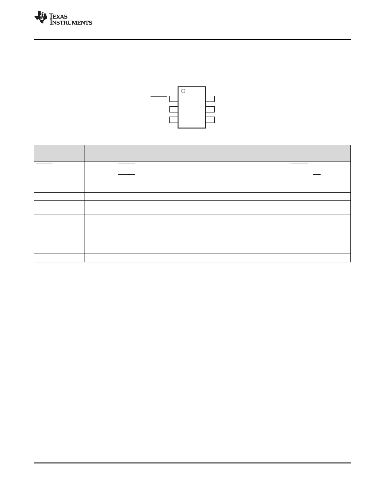
5 Pin Configuration and Functions
DBV PACKAGE
SOT-23
(TOP VIEW)
Pin Functions
PIN
NAME NO.
RESET 1 O RESET is an open-drain output that is driven to a low impedance state when RESET is asserted
GND 2 — Ground
MR 3 I Driving the manual reset pin (MR) low asserts RESET. MR is internally tied to VDDby a 90kΩ pullup
C
T
4 I Reset period programming pin. Connecting this pin to VDDthrough a 40-kΩ to 200-kΩ resistor or
SENSE 5 I This pin is connected to the voltage to be monitored. If the voltage at this terminal drops below the
V
DD
6 I Supply voltage. It is good analog design practice to place a 0.1-μF ceramic capacitor close to this pin.
I/O DESCRIPTION
(either the SENSE input is lower than the threshold voltage (VIT) or the MR pin is set to a logic low).
RESET remains low (asserted) for the reset period after both SENSE is above VITand MR is set to a
logic high. A pullup resistor from 10 kΩ to 1 MΩ should be used on this pin, and allows the reset pin to
attain voltages higher than VDD.
resistor.
leaving it open results in fixed delay times (see Switching Characteristics). Connecting this pin to a
ground referenced capacitor ≥ 100 pF gives a user-programmable delay time. See the Selecting the
Reset Delay Time section for more information.
threshold voltage VIT, then RESET is asserted.
Copyright © 2008–2014, Texas Instruments Incorporated Submit Documentation Feedback 3
Product Folder Links: TPS3808-EP
TPS3808-EP
SBVS103D –APRIL 2008–REVISED DECEMBER 2014
www.ti.com
6 Specifications
6.1 Absolute Maximum Ratings
Over operating junction temperature range, unless otherwise noted.
Input voltage, V
CTvoltage, V
Other voltage: V
RESET pin current 5 mA
Operating junction temperature, T
Storage temperature, T
(1) Stresses beyond those listed under Absolute Maximum Ratings may cause permanent damage to the device. These are stress ratings
only, which do not imply functional operation of the device at these or any other conditions beyond those indicated under Recommended
Operating Conditions. Exposure to absolute-maximum-rated conditions for extended periods may affect device reliability.
(2) As a result of the low dissipated power in this device, it is assumed that TJ= TA.
CT
DD
RESET
, VMR, V
stg
SENSE
(2)
J
6.2 ESD Ratings
Human body model (HBM), per ANSI/ESDA/JEDEC JS-001, all pins
V
(ESD)
(1) JEDEC document JEP155 states that 500-V HBM allows safe manufacturing with a standard ESD control process.
(2) JEDEC document JEP157 states that 250-V CDM allows safe manufacturing with a standard ESD control process.
Electrostatic discharge V
Charged device model (CDM), per JEDEC specification JESD22-C101, all ±1000
(2)
pins
(1)
MIN MAX UNIT
–0.3 7.0
–0.3 VDD+ 0.3 V
–0.3 7
–55 150
–65 150
°C
VALUE UNIT
(1)
±3000
6.3 Recommended Operating Conditions
over operating free-air temperature range (unless otherwise noted)
MIN NOM MAX UNIT
V
DD
Power-up reset voltage VOL(max) = 0.2 V, I
Input supply range 1.7 6.5 V
= 15 μA 0.8 V
RESET
6.4 Thermal Information
TPS3808-EP
THERMAL METRIC
R
θJA
R
θJC(top)
R
θJB
ψ
JT
ψ
JB
Junction-to-ambient thermal resistance 180.9
Junction-to-case (top) thermal resistance 117.8
Junction-to-board thermal resistance 27.8 °C/W
Junction-to-top characterization parameter 1.12
Junction-to-board characterization parameter 27.3
(1) For more information about traditional and new thermal metrics, see the IC Package Thermal Metrics application report, SPRA953.
(1)
DBV UNIT
6 PINS
4 Submit Documentation Feedback Copyright © 2008–2014, Texas Instruments Incorporated
Product Folder Links: TPS3808-EP
www.ti.com
6.5 Electrical Characteristics
1.7 V ≤ VDD≤ 6.5 V, R
otherwise noted. Typical values are at TJ= +25°C.
PARAMETER TEST CONDITIONS MIN TYP MAX UNIT
V
DD
I
DD
V
OL
V
IT
V
HYS
R
I
SENSE
I
OH
C
IN
V
IL
V
IH
θ
JA
(1) The lowest supply voltage (VDD) at which RESET becomes active. T
Input supply range 1.7 6.5 V
Supply current (current into VDDpin) μA
Low-level output voltage
Power-up reset voltage
Negative-going input
threshold accuracy
Hysteresis on VITpin V
MR Internal pullup resistance 70 90 kΩ
MR
Input current at
SENSE pin
RESET leakage current V
Input capacitance,
any pin
MR logic low input 0 0.3 V
MR logic high input 0.7 V
Thermal resistance, junction-to-ambient 290 °C/W
LRESET
= 100 kΩ, C
= 50 pF, over operating temperature range (TJ= –55°C to +125°C), unless
LRESET
VDD= 3.3 V, RESET not asserted
MR, RESET, CTopen
VDD= 6.5 V, RESET not asserted
MR, RESET, CTopen
1.3 V ≤ VDD< 1.8 V, IOL= 0.4 mA 0.3
1.8 V ≤ VDD≤ 6.5 V, IOL= 1.0 mA 0.4 V
(1)
VOL(max) = 0.2 V, I
TPS3808G01 –2.0% ±1.0% +2.0%
VIT≤ 3.3 V –1.7% ±0.5% +1.7%
3.3 V < VIT≤ 5.0 V –2.0% ±1.0% +2.0%
TPS3808G01 1.5% 3.0%
Fixed versions 1.0% 2.5%
TPS3808G01 V
Fixed versions V
= V
SENSE
SENSE
RESET
IT
= 6.5 V 1.7 μA
= 6.5 V, RESET not asserted 300 nA
CTpin VIN= 0 V to V
Other pins VIN= 0 V to 6.5 V 5
DD
rise(VDD)
SBVS103D –APRIL 2008–REVISED DECEMBER 2014
= 15 μA 0.8
RESET
–25 25 nA
DD
≥ 15 μs/V.
TPS3808-EP
2.4 5.0
2.7 6.0
5
DD
V
DD
IT
pF
V
6.6 Switching Characteristics
1.7 V ≤ VDD≤ 6.5 V, R
otherwise noted. Typical values are at TJ= +25°C.
PARAMETER TEST CONDITIONS MIN TYP MAX UNIT
Input pulse width to
t
w
RESET
t
RESET delay time See Timing Diagram
d
Propagation delay MR to RESET VIH= 0.7 VDD, VIL= 0.3 V
t
pHL
High-to-low level RESET
delay
LRESET
= 100 kΩ, C
= 50 pF, over operating temperature range (TJ= –55°C to +125°C), unless
LRESET
SENSE VIH= 1.05 VIT, VIL= 0.95 V
MR VIH= 0.7 VDD, VIL= 0.3 V
CT= Open 12 20 29
CT= V
DD
CT= 100 pF 0.75 1.25 1.8
CT= 180 nF 0.7 1.2 1.8 s
SENSE to RESET VIH= 1.05 VIT, VIL= 0.95 V
DD
DD
IT
20
0.00
μs
1
180 300 440 ms
150 ns
IT
20 μs
Copyright © 2008–2014, Texas Instruments Incorporated Submit Documentation Feedback 5
Product Folder Links: TPS3808-EP
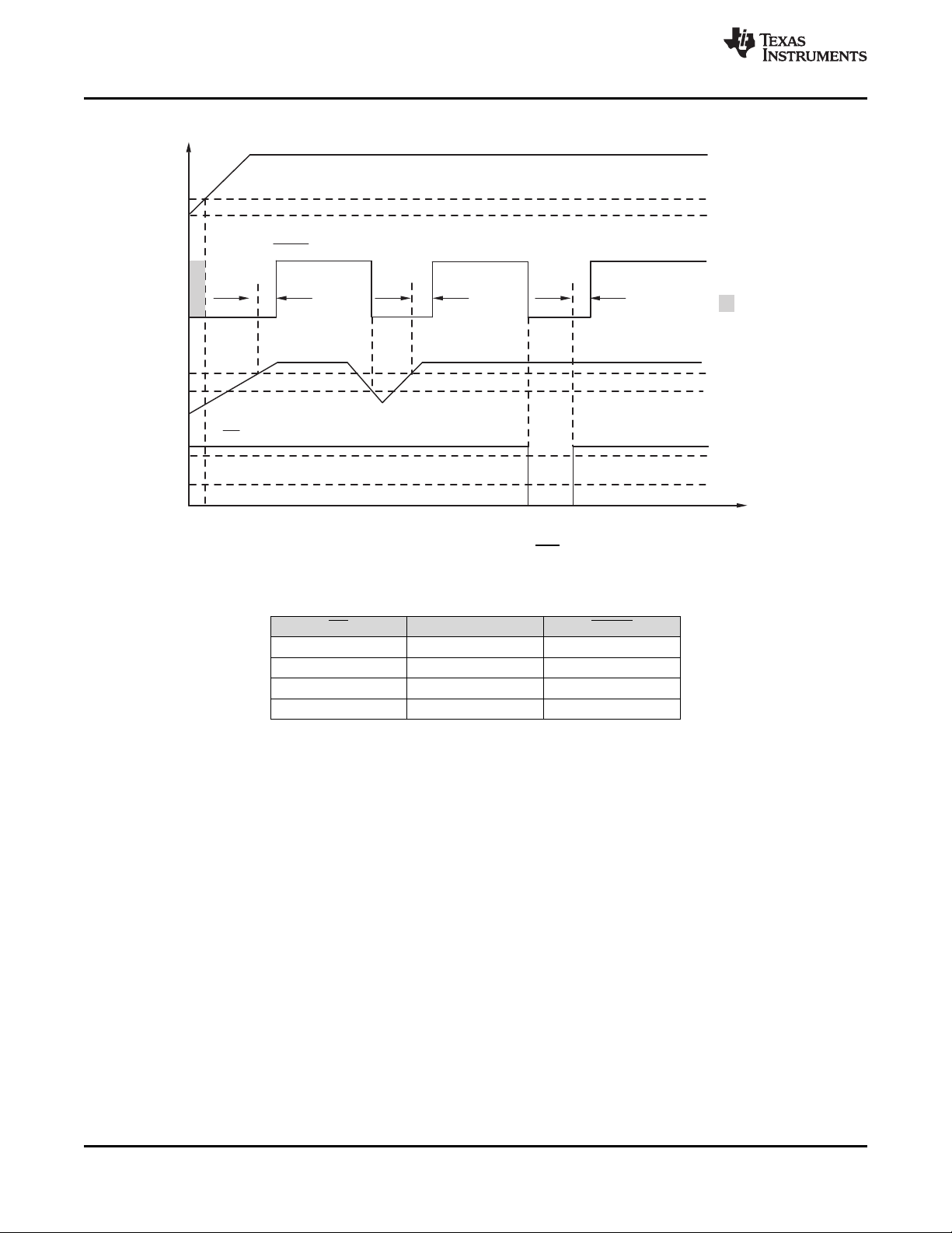
Time
0.8V
0.0V
VIT+ V
HYS
V
IT
0.7V
DD
0.3V
DD
MR
SENSE
RESET
V
DD
t
D
t
D
t
D
tD= Reset Delay
= Undefined State
TPS3808-EP
SBVS103D –APRIL 2008–REVISED DECEMBER 2014
www.ti.com
Figure 1. TPS3808 Timing Diagram Showing MR and SENSE Reset Timing
Table 1. Truth Table
MR SENSE > V
IT
L 0 L
L 1 L
H 0 L
H 1 H
RESET
6 Submit Documentation Feedback Copyright © 2008–2014, Texas Instruments Incorporated
Product Folder Links: TPS3808-EP
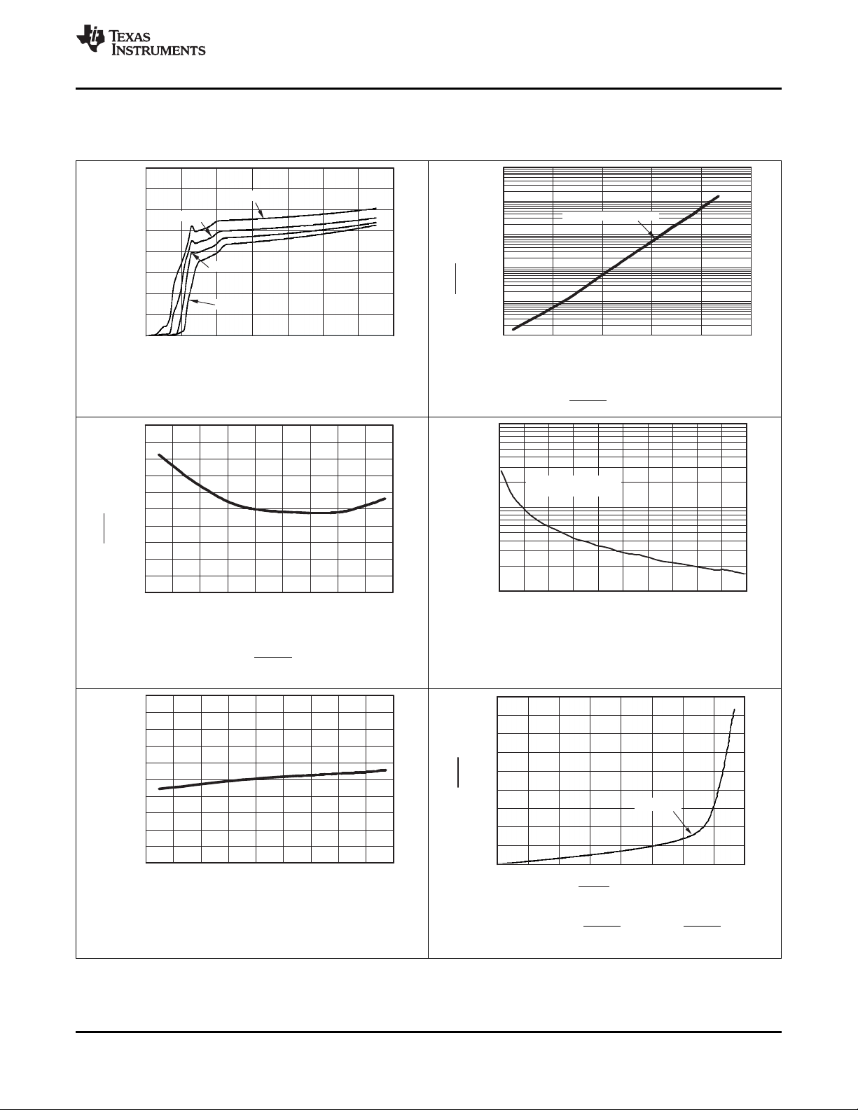
1.0
0.8
0.6
0.4
0.2
0
10 30 50 70 90 110 130
Temperature (°C)
−50 −30 −10
−1.0
−0.8
−0.6
−0.4
−0.2
Normalized V
IT
(%)
4.5
4.0
3.5
3.0
2.5
2.0
1.5
1.0
0.5
0
0 0.5 1.0 1.5 2.0 2.5 3.0 3.5 4.0
V
OL
Low−Level RESET Voltage (V)
VDD= 1.8V
RESET
Current (mA)
10
8
6
4
2
0
10 30 50 70 90 110 130
Temperature (°C)
−50 −30 −10
−10
−8
−6
−4
−2
Normalized RESET Timeout Period (%)
100
10
1
0 5 10 15 20 30 35 4525
Overdrive (%VIT)
5040
Transient Duration below V
IT
(µs)
RESET OCCURS
ABOVE THE CURVE
100
10
1
0.1
0.01
0.001
0.0001 0.001 0.01 0.1
CT(µF)
101
−40°C, +25°C, +125°C
RESET Timeout (sec)
0 1 2 3 4 5 6 7
4.0
3.5
3.0
2.5
2.0
1.5
1.0
0.5
0
−40
_
C
+25_C
+85_C
+125_C
I
DD
(µA)
VDD (V)
www.ti.com
6.7 Typical Characteristics
At TJ= +25°C, VDD= 3.3 V, R
LRESET
= 100kΩ, and C
= 50pF, unless otherwise noted.
LRESET
TPS3808-EP
SBVS103D –APRIL 2008–REVISED DECEMBER 2014
Figure 2. Supply Current vs Supply Voltage
Figure 3. RESET Timeout Period vs C
T
CT= Open, CT= VDD, CT= Any
Figure 4. Normalized RESET Timeout Period vs Figure 5. Maximum Transient Duration at Sense vs Sense
Temperature Threshold Overdrive Voltage
Copyright © 2008–2014, Texas Instruments Incorporated Submit Documentation Feedback 7
Figure 6. Normalized Sense Threshold Voltage (VIT) vs
Temperature
Figure 7. Low-Level RESET Voltage vs RESET Current
Product Folder Links: TPS3808-EP
0 0.5 1.0 1.5 2.0 2.5 3.0 3.5 4.0 4.5 5.0
0.8
0.7
0.6
0.5
0.4
0.3
0.2
0.1
0
V
OL
Low−Level RESET Voltage (V)
RESET Current (mA)
VDD= 3.3V
VDD= 6.5V
TPS3808-EP
SBVS103D –APRIL 2008–REVISED DECEMBER 2014
Typical Characteristics (continued)
www.ti.com
At TJ= +25°C, VDD= 3.3 V, R
= 100kΩ, and C
LRESET
= 50pF, unless otherwise noted.
LRESET
Figure 8. Low-Level RESET Voltage vs RESET Current
8 Submit Documentation Feedback Copyright © 2008–2014, Texas Instruments Incorporated
Product Folder Links: TPS3808-EP

Adjustable Voltage Version Fixed Voltage Version
Reset
Logic
Timer
+
-
90k
V
DD
V
DD
GND
0.4V
V
REF
SENSE
MR
C
T
RESET
TPS3808G01
Adjustable Voltage
Reset
Logic
Timer
+
-
90k
V
DD
V
DD
GND
0.4V
V
REF
SENSE
MR
C
T
RESET
R
1
R
2
R1+ R2= 4M
W
TPS3808-EP
www.ti.com
SBVS103D –APRIL 2008–REVISED DECEMBER 2014
7 Detailed Description
7.1 Overview
The TPS3808 microprocessor supervisory product family is designed to assert a RESET signal when either the
SENSE pin voltage drops below VITor the manual reset (MR) is driven low. The RESET output remains asserted
for a user-adjustable time after both the manual reset (MR) and SENSE voltages return above the respective
thresholds.
7.2 Functional Block Diagrams
7.3 Feature Description
A broad range of voltage threshold and reset delay time adjustments are available for the TPS3808 device,
allowing these devices to be used in a wide array of applications. Reset threshold voltages can be factory-set
from 0.82 V to 3.3 V or from 4.4 V to 5.0 V, while the TPS3808G01 can be set to any voltage above 0.405 V
using an external resistor divider. Two preset delay times are also user-selectable: connecting the CTpin to V
results in a 300 ms reset delay, while leaving the CTpin open yields a 20-ms reset delay. In addition, connecting
a capacitor between CTand GND allows the designer to select any reset delay period from 1.25 ms to 10 s.
7.4 Device Functional Modes
The TPS3808 has two functional modes:
• MR high: in this mode, RESET is high or low depending on the value of the SENSE pin relative to VIT.
• MR low: in this mode, RESET is held low regarldess of the value of the SENSE pin.
Copyright © 2008–2014, Texas Instruments Incorporated Submit Documentation Feedback 9
Product Folder Links: TPS3808-EP
DD

V
IN
TPS3808G01
V
DD
SENSE
GND
RESET
R
1
R
2
1nF
V =(1+)0.405IT¢
R1
R2
V
OUT
TPS3808-EP
SBVS103D –APRIL 2008–REVISED DECEMBER 2014
www.ti.com
8 Application and Implementation
NOTE
Information in the following applications sections is not part of the TI component
specification, and TI does not warrant its accuracy or completeness. TI’s customers are
responsible for determining suitability of components for their purposes. Customers should
validate and test their design implementation to confirm system functionality.
8.1 Application Information
The following sections describe in detail how to properly use this device depending on the requirements of the
final application.
8.1.1 SENSE Input
The SENSE input provides a terminal at which any system voltage can be monitored. If the voltage on this pin
drops below VIT, then RESET is asserted. The comparator has a built-in hysteresis to ensure smooth RESET
assertions and de-assertions. It is good analog design practice to put a 1-nF to 10-nF bypass capacitor on the
SENSE input to reduce sensitivity to transients and layout parasitics.
The TPS3808 device is relatively immune to short negative transients on the SENSE pin. Sensitivity to transients
is dependent on threshold overdrive, as shown in the Maximum Transient Duration at Sense vs Sense Threshold
Overdrive Voltage graph (Figure 5) in Typical Characteristics.
The TPS3808G01 can be used to monitor any voltage rail down to 0.405 V using the circuit shown in Figure 9.
Figure 9. Using the TPS3808G01 to Monitor a User-Defined Threshold Voltage
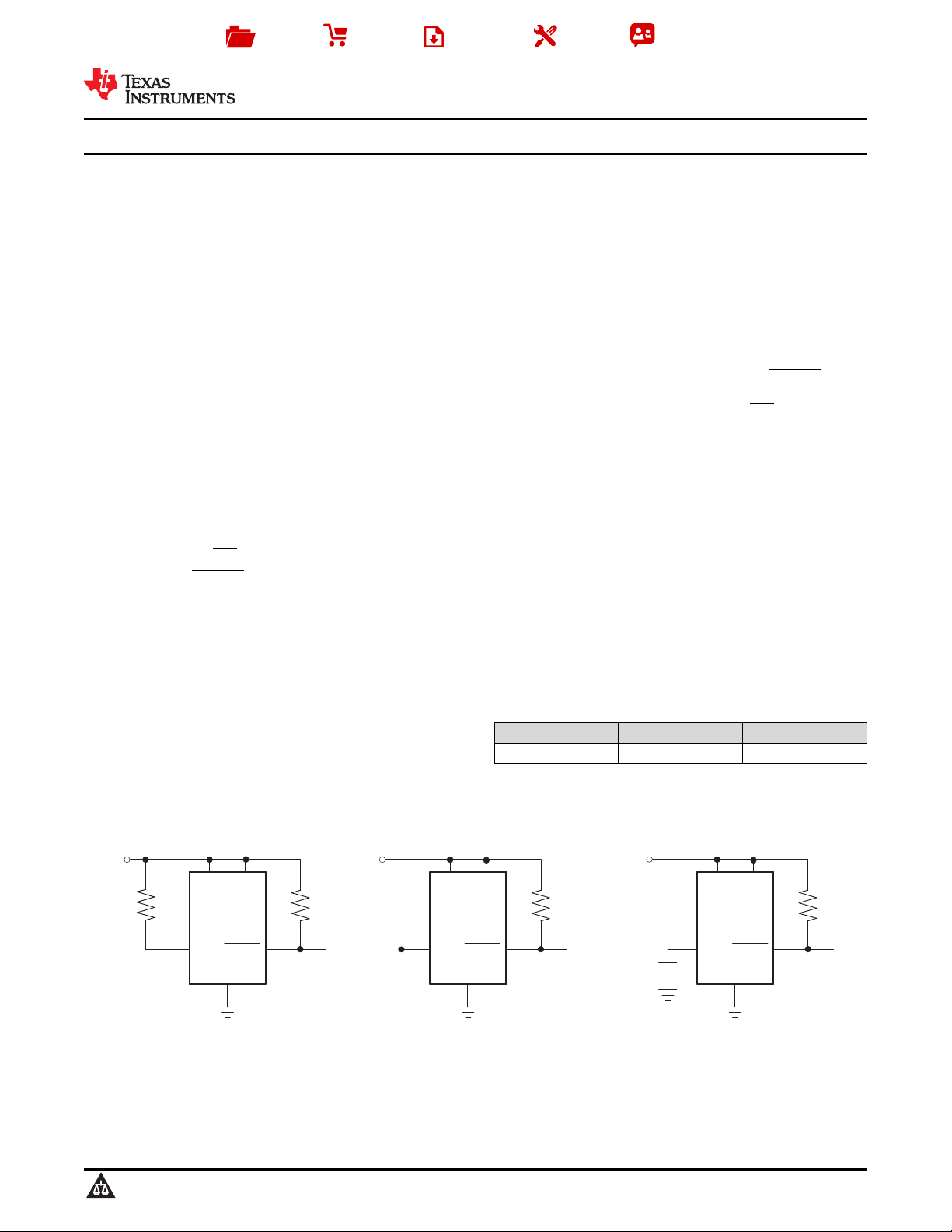
8.1.2 Selecting the RESET Delay Time
The TPS3808 has three options for setting the RESET delay time as shown in Figure 10. Figure 10a shows the
configuration for a fixed 300-ms typical delay time by tying CTto VDD; a resistor from 40 kΩ to 200 kΩ must be
used. Supply current is not affected by the choice of resistor. Figure 10b shows a fixed 20-ms delay time by
leaving the CTpin open. Figure 10c shows a ground referenced capacitor connected to CTfor a user-defined
program time between 1.25 ms and 10 s.
10 Submit Documentation Feedback Copyright © 2008–2014, Texas Instruments Incorporated
Product Folder Links: TPS3808-EP

1.2V 3.3V
TPS3808G12 TPS3808G33 DSP
SENSE V
DD
V
DD
SENSE
V
I/OVCORE
GPIO
GNDGNDGND
RESET MR
C
T
C
T
RESET
CT(nF) tD(s) 0.5 103(s) 175
=
[ ]
–
× ×
-
Delay (s) = CT (nF) + 0.5 x 10⁻³ (s)
20ms Delay
300ms Delay
(c)
(b)
(a)
175
3.3V
TPS3808G33
V
DD
SENSE
CTRESET
3.3V
TPS3808G33
V
DD
SENSE
C
T
C
T
RESET
3.3V
TPS3808G33
V
DD
SENSE
C
T
50k
Ω
RESET
TPS3808-EP
www.ti.com
SBVS103D –APRIL 2008–REVISED DECEMBER 2014
Application Information (continued)
Figure 10. Configuration Used to Set the RESET Delay Time
The capacitor CTshould be ≥ 100 pF nominal value in order for the TPS3808xxx to recognize that the capacitor
is present. The capacitor value for a given delay time can be calculated using Equation 1.
(1)
The reset delay time is determined by the time it takes an on-chip precision 220-nA current source to charge the
external capacitor to 1.23 V. When a RESET is asserted the capacitor is discharged. When the RESET
conditions are cleared, the internal current source is enabled and begins to charge the external capacitor. When
the voltage on this capacitor reaches 1.23 V, RESET is deasserted. Note that a low-leakage type capacitor such
as a ceramic should be used, and that stray capacitance around this pin may cause errors in the reset delay
time.
8.1.3 Manual RESET(MR) Input
The manual reset (MR) input allows a processor or other logic circuits to initiate a reset. A logic low (0.3 VDD) on
MR causes RESET to assert. After MR returns to a logic high and SENSE is above its reset threshold, RESET is
de-asserted after the user defined reset delay expires. Note that MR is internally tied to VDDusing a 90-kΩ
resistor so this pin can be left unconnected if MR will not be used.
See Figure 11 for how MR can be used to monitor multiple system voltages. Note that if the logic signal driving
MR does not go fully to VDD, there will be some additional current draw into VDDas a result of the internal pullup
resistor on MR. To minimize current draw, a logic-level FET can be used as illustrated in Figure 12.
Figure 11. Using MR to Monitor Multiple System Voltages
Copyright © 2008–2014, Texas Instruments Incorporated Submit Documentation Feedback 11
Product Folder Links: TPS3808-EP

3.3V
TPS3808xxx
VDDSENSE
MR
90kW
GND
TPS3808-EP
SBVS103D –APRIL 2008–REVISED DECEMBER 2014
Application Information (continued)
www.ti.com
Figure 12. Using an External MOSFET to Minimize IDDWhen MR Signal Does Not Go to V
DD
8.1.4 RESET Output
RESET remains high (unasserted) as long as SENSE is above its threshold (VIT) and the manual reset (MR) is
logic high. If either SENSE falls below VITor MR is driven low, RESET is asserted, driving the RESET pin to a
low impedance.
Once MR is again logic high and SENSE is above VIT+ V
(the threshold hysteresis), a delay circuit is enabled
HYS
which holds RESET low for a specified reset delay period. Once the reset delay has expired, the RESET pin
goes to a high impedance state. The pullup resistor from the open-drain RESET to the supply line can be used to
allow the reset signal for the microprocessor to have a voltage higher than VDD(up to 6.5 V). The pullup resistor
should be no smaller than 10 kΩ as a result of the finite impedance of the RESET line.
12 Submit Documentation Feedback Copyright © 2008–2014, Texas Instruments Incorporated
Product Folder Links: TPS3808-EP

1 MŸ
V
DD
SENSE
GND
RESET
MR
GND
TPS3808G33
C
T
RESET
V
DD
3.3 V PROCESSOR
0.1 µF
+3.3 V
TPS3808-EP
www.ti.com
SBVS103D –APRIL 2008–REVISED DECEMBER 2014
8.2 Typical Application
A typical application of the TPS3808G33 used with a 3.3 V processor is shown in Figure 13. The open-drain
RESET output is typically connected to the RESET input of a microprocessor. A pullup resistor must be used to
hold this line high when RESET is not asserted. The RESET output is undefined for voltage below 0.8 V, but this
is normally not a problem since most microprocessors do not function below this voltage.
Figure 13. Typical Application of the TPS3808 with a 3.3 V Processor
8.2.1 Design Requirements
The TPS3808 is intended to drive the RESET input of a microprocessor. The RESET pin is pulled high with a 1
MΩ resistor and the reset delay time is controlled by CTdepending on the reset requirement times of the
microprocessor. In this case, CTis left open for a typical reset delay time of 20 ms.
8.2.2 Detailed Design Procedure
The main constraint for this application is the reset delay time. In this case, since CTis open, it is set to 20 ms. A
0.1 µF decoupling capacitor is connected to the VDDpin and a 1 MΩ resistor is used to pull-up the RESET pin
high. The MR pin can be connected to an external signal if desired.
Copyright © 2008–2014, Texas Instruments Incorporated Submit Documentation Feedback 13
Product Folder Links: TPS3808-EP

100
10
1
0 5 10 15 20 30 35 4525
Overdrive (%VIT)
5040
Transient Duration below V
IT
(µs)
RESET OCCURS
ABOVE THE CURVE
TPS3808-EP
SBVS103D –APRIL 2008–REVISED DECEMBER 2014
Typical Application (continued)
8.2.3 Application Curve
Figure 14. Maximum Transient Duration at Sense vs Sense Threshold Overdrive Voltage
www.ti.com
14 Submit Documentation Feedback Copyright © 2008–2014, Texas Instruments Incorporated
Product Folder Links: TPS3808-EP

C
IN
GND
V
DD
GND
V
DD
C
T
SENSE
RESET
MR
VIAS USED TO CONNECT PINS FOR APPLICATION SPECIFIC CONNECTIONS
TPS3808-EP
www.ti.com
SBVS103D –APRIL 2008–REVISED DECEMBER 2014
9 Power Supply Recommendations
These devices are designed to operate from an input supply with a voltage range between 1.7 and 6.5 V. Use a
low-impedance power supply to eliminate inaccuracies caused by the current during the voltage reference
refresh.
10 Layout
10.1 Layout Guidelines
Make sure the connection to the VDDpin is low impedance. Place a 0.1-µF ceramic capacitor near the VDDpin.
10.2 Layout Example
The layout example in Figure 15 shows how the TPS3808 is laid out on a PCB for a 20 ms delay.
Figure 15. Layout Example for a 20 ms Delay
Copyright © 2008–2014, Texas Instruments Incorporated Submit Documentation Feedback 15
Product Folder Links: TPS3808-EP

TPS3808-EP
SBVS103D –APRIL 2008–REVISED DECEMBER 2014
www.ti.com
11 Device and Documentation Support
11.1 Trademarks
All trademarks are the property of their respective owners.
11.2 Electrostatic Discharge Caution
These devices have limited built-in ESD protection. The leads should be shorted together or the device placed in conductive foam
during storage or handling to prevent electrostatic damage to the MOS gates.
11.3 Glossary
SLYZ022 — TI Glossary.
This glossary lists and explains terms, acronyms, and definitions.
12 Mechanical, Packaging, and Orderable Information
The following pages include mechanical, packaging, and orderable information. This information is the most
current data available for the designated devices. This data is subject to change without notice and revision of
this document. For browser-based versions of this data sheet, refer to the left-hand navigation.
16 Submit Documentation Feedback Copyright © 2008–2014, Texas Instruments Incorporated
Product Folder Links: TPS3808-EP

PACKAGE OPTION ADDENDUM
www.ti.com
10-Dec-2020
PACKAGING INFORMATION
Orderable Device Status
TPS3808G01MDBVTEP ACTIVE SOT-23 DBV 6 250 RoHS & Green NIPDAU Level-1-260C-UNLIM -55 to 125 NXS
TPS3808G33MDBVREP ACTIVE SOT-23 DBV 6 3000 RoHS & Green NIPDAU Level-1-260C-UNLIM -55 to 125 CHK
V62/08607-01XE ACTIVE SOT-23 DBV 6 250 RoHS & Green NIPDAU Level-1-260C-UNLIM -55 to 125 NXS
V62/08607-09XE ACTIVE SOT-23 DBV 6 3000 RoHS & Green NIPDAU Level-1-260C-UNLIM -55 to 125 CHK
(1)
The marketing status values are defined as follows:
ACTIVE: Product device recommended for new designs.
LIFEBUY: TI has announced that the device will be discontinued, and a lifetime-buy period is in effect.
NRND: Not recommended for new designs. Device is in production to support existing customers, but TI does not recommend using this part in a new design.
PREVIEW: Device has been announced but is not in production. Samples may or may not be available.
OBSOLETE: TI has discontinued the production of the device.
Package Type Package
(1)
Drawing
Pins Package
Qty
Eco Plan
(2)
Lead finish/
Ball material
(6)
MSL Peak Temp
(3)
Op Temp (°C) Device Marking
(4/5)
(2)
RoHS: TI defines "RoHS" to mean semiconductor products that are compliant with the current EU RoHS requirements for all 10 RoHS substances, including the requirement that RoHS substance
do not exceed 0.1% by weight in homogeneous materials. Where designed to be soldered at high temperatures, "RoHS" products are suitable for use in specified lead-free processes. TI may
reference these types of products as "Pb-Free".
RoHS Exempt: TI defines "RoHS Exempt" to mean products that contain lead but are compliant with EU RoHS pursuant to a specific EU RoHS exemption.
Green: TI defines "Green" to mean the content of Chlorine (Cl) and Bromine (Br) based flame retardants meet JS709B low halogen requirements of <=1000ppm threshold. Antimony trioxide based
flame retardants must also meet the <=1000ppm threshold requirement.
(3)
MSL, Peak Temp. - The Moisture Sensitivity Level rating according to the JEDEC industry standard classifications, and peak solder temperature.
(4)
There may be additional marking, which relates to the logo, the lot trace code information, or the environmental category on the device.
(5)
Multiple Device Markings will be inside parentheses. Only one Device Marking contained in parentheses and separated by a "~" will appear on a device. If a line is indented then it is a continuation
of the previous line and the two combined represent the entire Device Marking for that device.
(6)
Lead finish/Ball material - Orderable Devices may have multiple material finish options. Finish options are separated by a vertical ruled line. Lead finish/Ball material values may wrap to two
lines if the finish value exceeds the maximum column width.
Important Information and Disclaimer:The information provided on this page represents TI's knowledge and belief as of the date that it is provided. TI bases its knowledge and belief on information
provided by third parties, and makes no representation or warranty as to the accuracy of such information. Efforts are underway to better integrate information from third parties. TI has taken and
Samples
Addendum-Page 1

PACKAGE OPTION ADDENDUM
www.ti.com
continues to take reasonable steps to provide representative and accurate information but may not have conducted destructive testing or chemical analysis on incoming materials and chemicals.
TI and TI suppliers consider certain information to be proprietary, and thus CAS numbers and other limited information may not be available for release.
10-Dec-2020
In no event shall TI's liability arising out of such information exceed the total purchase price of the TI part(s) at issue in this document sold by TI to Customer on an annual basis.
OTHER QUALIFIED VERSIONS OF TPS3808-EP :
Catalog: TPS3808
•
Automotive: TPS3808-Q1
•
NOTE: Qualified Version Definitions:
Catalog - TI's standard catalog product
•
Automotive - Q100 devices qualified for high-reliability automotive applications targeting zero defects
•
Addendum-Page 2

PACKAGE MATERIALS INFORMATION
www.ti.com 5-Jan-2021
TAPE AND REEL INFORMATION
*All dimensions are nominal
Device Package
TPS3808G01MDBVTEP SOT-23 DBV 6 250 179.0 8.4 3.2 3.2 1.4 4.0 8.0 Q3
TPS3808G33MDBVREP SOT-23 DBV 6 3000 179.0 8.4 3.2 3.2 1.4 4.0 8.0 Q3
Type
Package
Drawing
Pins SPQ Reel
Diameter
(mm)
Reel
Width
W1 (mm)
A0
(mm)B0(mm)K0(mm)P1(mm)W(mm)
Quadrant
Pin1
Pack Materials-Page 1

PACKAGE MATERIALS INFORMATION
www.ti.com 5-Jan-2021
*All dimensions are nominal
Device Package Type Package Drawing Pins SPQ Length (mm) Width (mm) Height (mm)
TPS3808G01MDBVTEP SOT-23 DBV 6 250 200.0 183.0 25.0
TPS3808G33MDBVREP SOT-23 DBV 6 3000 200.0 183.0 25.0
Pack Materials-Page 2

PACKAGE OUTLINE
PIN 1
INDEX AREA
2X 0.95
1.9
0.50
6X
0.25
0.2 C A B
A
3.05
2.75
SOT-23 - 1.45 mm max heightDBV0006A
SMALL OUTLINE TRANSISTOR
C
0.1 C
1.45 MAX
(1.1)
0.15
0.00
TYP
SCALE 4.000
3.0
2.6
1.75
1.45
1
2
3
B
6
5
4
0.25
GAGE PLANE
8
TYP
0
0.6
0.3
TYP
SEATING PLANE
0.22
0.08
TYP
4214840/B 03/2018
NOTES:
1. All linear dimensions are in millimeters. Any dimensions in parenthesis are for reference only. Dimensioning and tolerancing
per ASME Y14.5M.
2. This drawing is subject to change without notice.
3. Body dimensions do not include mold flash or protrusion. Mold flash and protrusion shall not exceed 0.15 per side.
4. Leads 1,2,3 may be wider than leads 4,5,6 for package orientation.
5. Refernce JEDEC MO-178.
www.ti.com

EXAMPLE BOARD LAYOUT
SOT-23 - 1.45 mm max heightDBV0006A
SMALL OUTLINE TRANSISTOR
2X (0.95)
(R0.05) TYP
SOLDER MASK
OPENING
6X (0.6)
6X (1.1)
PKG
1
2
3
(2.6)
LAND PATTERN EXAMPLE
EXPOSED METAL SHOWN
SCALE:15X
METAL
METAL UNDER
SOLDER MASK
6
SYMM
5
4
SOLDER MASK
OPENING
EXPOSED METAL
0.07 MAX
ARROUND
NON SOLDER MASK
DEFINED
(PREFERRED)
EXPOSED METAL
0.07 MIN
ARROUND
SOLDER MASK
DEFINED
SOLDER MASK DETAILS
NOTES: (continued)
6. Publication IPC-7351 may have alternate designs.
7. Solder mask tolerances between and around signal pads can vary based on board fabrication site.
4214840/B 03/2018
www.ti.com

1
EXAMPLE STENCIL DESIGN
SOT-23 - 1.45 mm max heightDBV0006A
SMALL OUTLINE TRANSISTOR
PKG
6X (1.1)
6X (0.6)
2X(0.95)
(R0.05) TYP
2
3
(2.6)
SOLDER PASTE EXAMPLE
BASED ON 0.125 mm THICK STENCIL
SCALE:15X
6
SYMM
5
4
4214840/B 03/2018
NOTES: (continued)
8. Laser cutting apertures with trapezoidal walls and rounded corners may offer better paste release. IPC-7525 may have alternate
design recommendations.
9. Board assembly site may have different recommendations for stencil design.
www.ti.com

IMPORTANT NOTICE AND DISCLAIMER
TI PROVIDES TECHNICAL AND RELIABILITY DATA (INCLUDING DATASHEETS), DESIGN RESOURCES (INCLUDING REFERENCE
DESIGNS), APPLICATION OR OTHER DESIGN ADVICE, WEB TOOLS, SAFETY INFORMATION, AND OTHER RESOURCES “AS IS”
AND WITH ALL FAULTS, AND DISCLAIMS ALL WARRANTIES, EXPRESS AND IMPLIED, INCLUDING WITHOUT LIMITATION ANY
IMPLIED WARRANTIES OF MERCHANTABILITY, FITNESS FOR A PARTICULAR PURPOSE OR NON-INFRINGEMENT OF THIRD
PARTY INTELLECTUAL PROPERTY RIGHTS.
These resources are intended for skilled developers designing with TI products. You are solely responsible for (1) selecting the appropriate
TI products for your application, (2) designing, validating and testing your application, and (3) ensuring your application meets applicable
standards, and any other safety, security, or other requirements. These resources are subject to change without notice. TI grants you
permission to use these resources only for development of an application that uses the TI products described in the resource. Other
reproduction and display of these resources is prohibited. No license is granted to any other TI intellectual property right or to any third party
intellectual property right. TI disclaims responsibility for, and you will fully indemnify TI and its representatives against, any claims, damages,
costs, losses, and liabilities arising out of your use of these resources.
TI’s products are provided subject to TI’s Terms of Sale (https:www.ti.com/legal/termsofsale.html) or other applicable terms available either
on ti.com or provided in conjunction with such TI products. TI’s provision of these resources does not expand or otherwise alter TI’s
applicable warranties or warranty disclaimers for TI products.IMPORTANT NOTICE
Mailing Address: Texas Instruments, Post Office Box 655303, Dallas, Texas 75265
Copyright © 2021, Texas Instruments Incorporated
 Loading...