

Page 1

User's Guide
SLVUA44–June 2014
TPS25940XEVM-635: Evaluation Module for TPS25940X
This user’s guide describes the evaluation module (EVM) for the Texas instruments TPS25940X devices.
TPS25940X devices are eFuse with true reverse blocking for power mux that operates from 2.7 V to 18 V,
the device has integrated back-to-back FETs with programmable undervoltage, overvoltage, reversevoltage, overcurrent and in-rush current protection features.
Contents
1 Introduction ................................................................................................................... 2
1.1 EVM Features....................................................................................................... 2
1.2 EVM Applications ................................................................................................... 2
2 Description.................................................................................................................... 2
3 Schematic..................................................................................................................... 3
4 General Configurations ..................................................................................................... 4
4.1 Physical Access..................................................................................................... 4
4.2 Test Equipment ..................................................................................................... 5
4.3 Test Setup ........................................................................................................... 6
4.4 Test Procedures .................................................................................................... 7
5 EVM Assembly Drawings and Layout Guidelines...................................................................... 12
6 Bill of Materials (BOM)..................................................................................................... 14
List of Figures
1 TPS25940XEVM Schematic ............................................................................................... 3
2 EVM Test Setup.............................................................................................................. 6
3 V
4 V
5 J4 = LO Current Limit Test Auto Retry (CH1) .......................................................................... 11
6 J9 = “No Jumper” Current Limit Test with Latch (CH2) ............................................................... 11
7 Top Side Placement ....................................................................................................... 12
8 Top Side Routing Layer ................................................................................................... 12
9 Bottom Side Routing Layer ............................................................................................... 13
1 TPS25940X EVM Options and Default Setting .......................................................................... 2
2 Input and Output Connector Functionality................................................................................ 4
3 Test Points Description ..................................................................................................... 4
4 Jumper and LED Descriptions ............................................................................................. 4
5 EVM Configuration Setting ................................................................................................. 5
6 Operational Range Setting for VIN1, VIN2 = 12 V, 5 V and 3.3 V .................................................... 7
7 PWR635 DMM Readings at Different Test Points....................................................................... 7
8 PWR635 Oscilloscope Setting for Ramp Up Voltage Test............................................................. 8
9 PWR635 Oscilloscope Settings for Current Limit Test................................................................ 10
10 PWR635 Jumper Setting for Current Limits ............................................................................ 10
11 TPS25940XEVM-635 Bill of Material ................................................................................... 14
Ramp Up Time for CH1 ............................................................................................... 9
OUT
Ramp Up Time for CH2 ............................................................................................... 9
OUT
List of Tables
SLVUA44–June 2014 TPS25940XEVM-635: Evaluation Module for TPS25940X
Submit Documentation Feedback
1
Copyright © 2014, Texas Instruments Incorporated
Page 2
Introduction
1 Introduction
The TPS25940XEVM allows reference circuit evaluation of TI's TPS25940X devices. The TPS25940X
devices are available with both latched and auto-retry operation.
1.1 EVM Features
• 2.7-V to 18.0-V (TYP) operation
– CH1 rising input voltage turn-on threshold – 10.5 V (TYP)
– CH1 falling input voltage turn-off threshold – 9.7 V (TYP)
– CH2 rising input voltage turn-on threshold – 2.3 V (TYP)
– CH2 falling input voltage turn-off threshold – 2.1 V (TYP)
• 0.6-A to 5.0-A programmable current limit
• Programmable undervoltage lockout, overvoltage
• Programmable V
• Latched-off TPS25940LRUV (CH2)
• Auto-Retry TPS25940ARUV (CH1)
• Pushbutton RESET signal
• On-board transorb for overvoltage input protection
• Schottky diode at output to minimize negative spike when load is removed
1.2 EVM Applications
• Solid state drives and hard disk drives
• PCIe, RAID, and NIC cards
• USB power switch
• Industrial
– PLCs
– Solid-state relays and FAN control
slew rate
OUT
www.ti.com
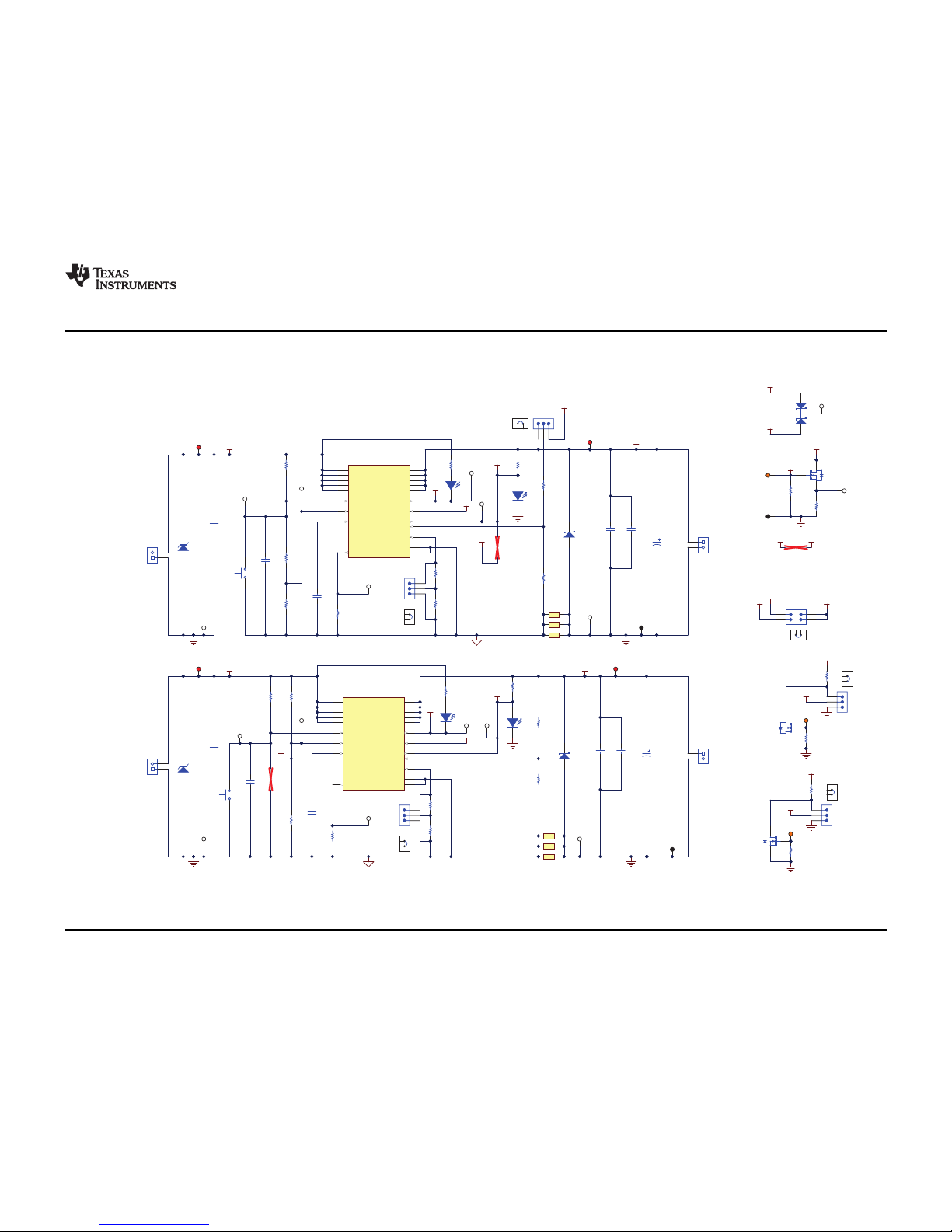
2 Description
The TPS25940XEVM-635 enables full evaluation of the TPS25940X devices. The EVM supports two
versions (Auto-retry and Latched) of the devices on two Channels (CH1 and CH2, respectively). Input
power is applied at J3 (CH1) and J8 (CH2), while J2 (CH1)/J7 (CH2) provide the output connection to the
load, refer to the schematic in Figure 1, and test setup in Figure 2.
D5/C1 (CH1), D9/C7 (CH2) provides input protection for TPS25940X (U1 and U2, respectively) while
D4/C2/C3/C4 (CH1), D8/C8/C9/C10 (CH2) provides output protection.
Table 1. TPS25940X EVM Options and Default Setting
Part Number EVM Function VINRange UVLO OVP Current Limit Fault Response
TPS25940XEVM-635 Current Limiter with DEVSLP 2.7 V–18 V 10.5 V 2.3 V (internal) 16.5 V 3.6 A 2.1 A 5.3 A Auto-retry Latched
S1 allows U1 and S2 allows U2 to be RESET or disabled. A power good (PG) indicator is provided by D3,
D6 for CH1 and CH2, respectively, and circuit faults can be observed with D2 and D6. Scaled channel
current can be monitored at TP11 and TP22 with a scale factor of 0.842 V/A.
2
TPS25940XEVM-635: Evaluation Module for TPS25940X SLVUA44–June 2014
CH1 CH2 LO setting No Jumper HI Setting CH1 CH2
Copyright © 2014, Texas Instruments Incorporated
Submit Documentation Feedback
Page 3
1nf
C12
475k
R20
SH-J9
1
2
3
J9
16.9k
R25
TP26
ILIM LO
ILIM HI
TP17
EN_UV2
TP18
OVP2
TP15
VIN2
TP16
VOUT2
Red
D6
Green
D7
10.0k
R5
TP10
P-LOAD-RTN
TP6
P-LOAD
330pF
C11
VIN2
TP7
I-LOAD
VOUT2
VOUT1
4
7,8
1,2,3
5,6,
30V
Q1
CSD17301Q5A
Pin1_CTRL-2
TP22
IMON2
FLTb-2
P-LOAD
2
1
S2
1nf
C6
475k
R4
SH-J4
1
2
3
J4
TP14
ILIM LO
ILIM HI
TP3
VIN1
TP2
VOUT1
Red
D2
Green
D3
330pF
C5
VIN1
VOUT1
Pin1_CTRL-1
TP11
IMON
FLTb-1
2
1
S1
0.1µF
C1
TP4
FLTb1
TP20
FLTb2
TP21
PG2
1 2
3 4
J5
VOUT1 VOUT2
SH-J5
TP12
TP25
TP24
TP13
VIN=2.7V-18V
IIN=0.6A-5.0A
VIN=2.7V-18V
IIN=0.6A-5.0A
VOUT=2.7V-18V
IOUT=0.6A-5.0A
VOUT=2.7V-18V
IOUT=0.6A-5.0A
1
2
3
Q3
1
2
3
J10
10k
R29
VIN2
100k
R24
SH-J10
Pin1_CTRL-2
1
2
3
Q2
10k
R21
VIN1
100k
R15
SH-J6
Pin1_CTRL-1
PG-1
PG-2
PG-1
PG-1
PG-2
TP1
SYS_PG
TP19
TP23
FLTb-1 Pin1_CTRL-2
VIN1
22k
R8
DNP
OVP-2
OVP-2
SH-J1
24.9k
R12
24.9k
R27
100k
R1
100k
R2
100k
R16
100k
R17
20V
D8
B320A-13-F
20V
D4
B320A-13-F
330µF
C10
16V
D9
16V
D5
4.7µFC24.7µF
C3
4.7µFC84.7µF
C9
DEVSLP
1
PGOOD
2
PGTH
3
OUT
4
OUT
5
OUT
6
OUT
7
OUT
8
IN
9
IN
10
IN
11
IN
12
IN
13
EN/UVLO
14
OVP
15
GND
16
ILIM
17
DVDT
18
IMON
19
FLTB
20
PAD
U1
TPS25940ARVC
DEVSLP
1
PGOOD
2
PGTH
3
OUT
4
OUT
5
OUT
6
OUT
7
OUT
8
IN
9
IN
10
IN
11
IN
12
IN
13
EN/UVLO
14
OVP
15
GND
16
ILIM
17
DVDT
18
IMON
19
FLTB
20
PAD
U2
TPS25940LRVC
0.1
R6
1
2
J3
1
2
J8
1
2
J2
1
2
J7
TP9
PG1
0.003
R7
DNP
TP5
OVP1
TP8
EN_UV1
475k
R3
475k
R18
475k
R19
16.9k
R9
32.4k
R13
48.7k
R22
DNP
32.4k
R26
47k
R11
47k
R23
EN/UVLO-1
OVP-1
DVDT-1
IMON-1
ILIM-1
PGTH-1
DVDT-2
IMON-2
ILIM-2
PGTH-2
EN/UVLO-2
1
2
3
J6
123
J1
SGND1
SGND2
Net-Tie
Net-Tie
Net-Tie
Net-Tie
Net-Tie
IMON-1
330µF
C4
16.9k
R10
16.2k
R14
16.2k
R28
Net-Tie
1µF
C7
1
3
2
D1
BAT54C-7-F
www.ti.com
Schematic
3 Schematic
Figure 1 shows the EVM schematic.
Figure 1. TPS25940XEVM Schematic
3
SLVUA44–June 2014 TPS25940XEVM-635: Evaluation Module for TPS25940X
Submit Documentation Feedback
Copyright © 2014, Texas Instruments Incorporated
Page 4
General Configurations
4 General Configurations
The following sections describe physical access, test equipment, test setup, and test procedures for the
EVM.
4.1 Physical Access
Table 2 lists the TPS25940XEVM-635 input and output connector functionality. Table 3 describes the test
point availability and Table 4 describes the jumper functionality.
Connector Label Description
J3 CH1 VIN1(+), GND(–) CH1 Input power supply to the EVM
J2 VOUT1(+),GND(–) CH1 Output power from the EVM
J8 CH2 VIN2(+), GND(–) CH2 Input power supply to the EVM
J7 VOUT2(+),GND(–) CH2 Output power from the EVM
Channe Test Points Label Description
l
CH1 TP3 VIN1 CH1 Input power supply to the EVM
TP8 EN_UV1 CH1 Active high enable and under voltage input
TP5 OVP1 CH1, Active high overvoltage input (>16.5V)
TP11 IMON1 CH1 Current monitor. Load current = 1.187 × voltage on TP11
TP2 VOUT1 CH1 Output from the EVM
TP9 PG1 CH1 Power good test point
TP4 FLTb1 CH1, Fault test point
TP12 GND GND
TP13 GND GND
TP14 GND GND
CH2 TP15 VIN2 CH2 Input power supply to the EVM
TP17 EN_UV2 CH2 Active high enable and under voltage input
TP18 OVP2 CH2, Active high overvoltage input
TP22 IMON2 CH2 Current monitor. Load current = 1.187 × voltage on TP22
TP16 VOUT2 CH2 Output from the EVM
TP21 PG2 CH2 Power good test point
TP20 FLTb2 CH2, Fault test point
TP24 GND GND
TP25 GND GND
TP26 GND GND
www.ti.com
Table 2. Input and Output Connector Functionality
Table 3. Test Points Description
Jumper Label Description
J1 J1 Priority Mux Setting (applicable to TPS25942XEVM-635)
J4 LO - HI CH2 Current Setting
J5 J5 PG1 and FLTb1 setting
J6 J6 DEVSLP1 Setting
J9 LO - HI CH2 Current Setting
J10 J10 DEVSLP2 Setting
D2 (Red) D2 CH1 circuit fault indicator. LED turns on when the internal MOSFET is disabled due to
4
TPS25940XEVM-635: Evaluation Module for TPS25940X SLVUA44–June 2014
Table 4. Jumper and LED Descriptions
a fault condition such as over load , short circuit, under voltage etc.
Submit Documentation Feedback
Copyright © 2014, Texas Instruments Incorporated
Page 5
www.ti.com
Use Table 5 to set the EVM in different configurations in order to achieve the desired functionality from the
TPS25940XEVM-635.
General Configurations
Table 4. Jumper and LED Descriptions (continued)
Jumper Label Description
D3 (Green) D3 CH1 Power good indicator. LED turns on when the voltage at TP2(VOUT1) is more
than 11 V
D6 (Red) D6 CH2 circuit fault indicator. LED turns on when the internal MOSFET is disabled due to
a fault condition such as over load , short circuit, under voltage etc.
D7(Green) D9 CH2 Power good indicator. LED turns on when the voltage at TP2(VOUT1) is more
than 11 V
Table 5. EVM Configuration Setting
Jumper Location E-fuse with DevSleep
J4 1-2 Install jumper at this location for 5.3 A
current Limit for VIN1
2-3 Install jumper at this location for 3.6 A
current Limit for VIN1
OPEN If no jumper is installed default current
limit is 2.1 A for VIN1
J9 1-2 Install jumper at this location for 5.3 A
current Limit for VIN2
2-3 Install jumper at this location for 3.6 A
current Limit for VIN2
OPEN If no jumper is installed default current
limit is 2.1 A for VIN2
J5 1-2 OPEN
3-4
J1 1-2 Install Jumper to get PG1 from VOUT1
2-3 OPEN
J6 1-2 OPEN
2-3
J10 1-2 OPEN
2-3
4.2 Test Equipment
This section describes the power supply, meter, oscilloscope, and loads for testing this EVM.
4.2.1 Power Supplies
One adjustable power supply: 0-V to 20-V output, 0-A to 6-A output current limit.
4.2.2 Meters
One DMM minimum needed and may require more if simultaneous measurements are needed.
4.2.3 Oscilloscope
A DPO2024 or Lecroy 424 oscilloscope or equivalent, three 10X voltage probes, and a DC current probe.
4.2.4 Loads
One resistive load or equivalent which take up to 6 ADC load at 12 V and capable to do the output short.
SLVUA44–June 2014 TPS25940XEVM-635: Evaluation Module for TPS25940X
Submit Documentation Feedback
5
Copyright © 2014, Texas Instruments Incorporated
Page 6
+ -
J2
J7
R7
D9
Positive
Load
Negative
J3
Negative
Power
Supply
Positive
Negative
Power
Supply
Positive
J8
D5
TP
12
TP
13
TP
24
TP
25
U1
U2
DUT
PWR635
Positive
Load
Negative
Voltmeter
PRINT
HELP
ALPHA
SHIFT
ENTER
RUN
DGERF
I
AJBKC
L
7M8N9
O
DGDGD
G
D
G T3U
0V.WX
Y
Z
TAB
% UTILIZATION
HUB/MAU NIC
2
BNC
4Mb/s
Voltmeter
PRINT
HELP
ALPHA
SHIFT
ENTER
RUN
DGERF
I
AJBKC
L
7M8N9
O
DGDGD
G
D
G T3U
0V.WX
Y
Z
TAB
% UTILIZATION
HUB/MAU NIC
2
BNC
4Mb/s
Oscilloscope
Texas
Instruments
S1
S2
D3
D2
D7
D6
General Configurations
4.3 Test Setup
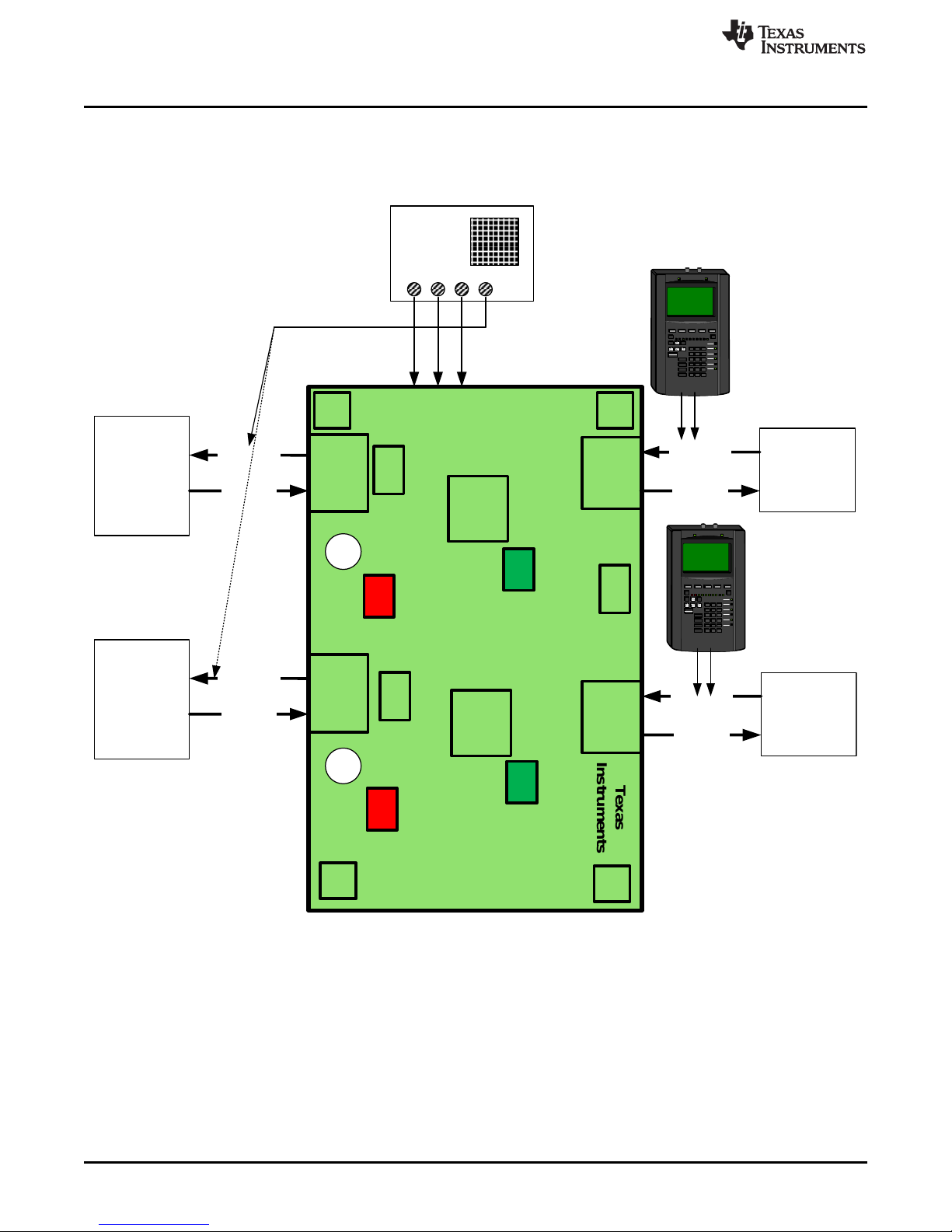
Figure 2 shows a typical test setup for the TPS25940XEVM. Connect J3/J8 to the power supply and J2/J7
to the load.
www.ti.com
Figure 2. EVM Test Setup
6
TPS25940XEVM-635: Evaluation Module for TPS25940X SLVUA44–June 2014
Copyright © 2014, Texas Instruments Incorporated
Submit Documentation Feedback
Page 7

www.ti.com
4.4 Test Procedures
Use the following steps for the test procedure:
1. The operational voltage range of the two rails VIN1 and VIN2 can be adjusted by changing a few
resistor settings, as listed in Table 6.
Table 6. Operational Range Setting for VIN1, VIN2 = 12 V, 5 V and 3.3 V
VIN Operational Range Rail: VIN1 or VIN2 R9 R13 R11 R22 R26
12 V: 10.5 V to 16 V VIN1 16.9k 32.4k 47k
(Default)
5 V: 4.6 V to 5.7 V VIN1 23.2k 105k 137k
3.3 V: 3 V to 3.8 V VIN1 48.7k 187k 237k
2.3 V to 15.5 V (Default) VIN2 NoPoP 32.4k
5 V: 4.6 V to 5.7 V VIN2 130k 100k
3.3 V: 3 V to 3.8 V VIN2 237k 169k
2. Turn on the power supply and set the power supply voltage to 12 V.
3. Turn off the power supply. Hook up CH1 and CH2 of the PWR635 assembly as shown in Figure 2.
4. Ensure that the output load is disabled and the power supply is set properly for the design under test
(DUT). Connect the negative probe of DMM to TP12 or TP25 (GND).
5. Turn on the power supply, only 1 channel at a time. Verify that the voltages shown in Table 7 are
obtained.
General Configurations
Table 7. PWR635 DMM Readings at Different Test Points
Voltage test on (CH1) Measured Voltage Reading Voltage tested on (CH2) Measured Voltage Reading
VIN1 (TP3) 12 ±0.3 VDC VIN2 (TP15) 12 ±0.3 VDC
EN_UV1 (TP8) 1.13 ±0.1 VDC EN_UV2 (TP17) 12 ±1 VDC
OVP1 (TP5) 0.742 ±0.1 VDC OVP2 (TP18) 0.742 ±0.1 VDC
IMON1 (TP11) 32.9 mV ±5 mV VDC IMON2 (TP22) 32.6 mV ±5 mV VDC
VOUT1 (TP2) 12 ±0.3 VDC VOUT2 (TP16) 12 ±0.3 VDC
PG1 (TP9) 2.40 ±0.2 VDC PG2 (TP21) 2.4 ±0.2 VDC
FLTb1 (TP4) 10.51 ±0.5 VDC FLTb2 (TP20) 10.5 ±0.5 VDC
SLVUA44–June 2014 TPS25940XEVM-635: Evaluation Module for TPS25940X
Submit Documentation Feedback
7
Copyright © 2014, Texas Instruments Incorporated
Page 8

General Configurations
4.4.1 Preliminary Tests
4.4.1.1 For CH1 (J3-J2)
• With the power supply set to 12 V on CH1, verify that the green PG LED (D3) is on. Press the EVM
RST switch, S1 and verify that the voltage at VOUT1 (TP2) starts falling slowly below 12 V and that the
green PG LED (D3) turns off and FLTb1 red LED (D2) turns ON. Release S1.
• Reduce the input voltage on VIN1 and monitor VOUT1, Verify that VOUT1 (TP2) starts falling and is
fully turned off when VIN1 (TP3) reaches 9.5 V (±0.5 V). Verify that the PG1 green LED (D3) turns off
and FLTb1 red LED (D2) turns ON.
• Increase the input voltage on VIN1 and monitor VOUT1, Verify that VOUT1 (TP2) starts increasing and
is fully turned off when VIN1 (TP3) reaches 16.5 V (±1 V). Verify that the PG1 green LED (D3) turns off
and FLTb1 red LED (D2) turns ON.
4.4.1.2 For CH2 (J8-J7)
• With the power supply set to 12 V on CH2, verify that the green PG LED (D7) is on. Depress the EVM
RST switch, S2 and verify that the voltage at VOUT2 (TP16) starts falling slowly below 12 V and that
the green PG LED (D7) turns off and red FLTb2 LED (D6) turns ON. Release S2.
• Reduce the input voltage on VIN2 and monitor VOUT2, verify that VOUT2 (TP16) starts falling and is
fully turned off when VIN2 (TP15) reaches 2.1 V (±0.3 V). Verify that the PG2 green LED (D7) turns off
and FLTb2 red LED (D6) turns ON.
• Increase the input voltage on VIN2 and monitor VOUT2, verify that VOUT2 (TP16) starts increasing
and is fully turned off when VIN2 (TP15) reaches 15.5 V (±1 V). Verify that the PG2 green LED (D7)
turns off and FLTb2 red LED (D6) turns ON.
• Turn off both the power supplies.
www.ti.com
4.4.1.3 Ramp up Time Test (CH1 and CH2)
• Verify ramp up time (CH1 and CH2, with only 1 channel powered at a time). Set up the oscilloscope
as shown in Table 8.
Table 8. PWR635 Oscilloscope Setting for Ramp Up Voltage Test
Oscilloscope setting CH1 Probe Points CH2 Probe Points
Channel 1 = 5 V/div TP2 = VOUT1 TP16 = VOUT2
Channel 2 = 5 V/div TP3 = VIN1 TP15 = VIN2
Channel 3 = 2 V/div TP8 = EN/UVLO1 TP17 = EN/UVLO2
Trigger source = Channel 1
Trigger level = 6.0 ±0.5 V
Trigger polarity = Positive
Trigger Mode = Single Sequence
Time base = 1 ms/div
8
TPS25940XEVM-635: Evaluation Module for TPS25940X SLVUA44–June 2014
Copyright © 2014, Texas Instruments Incorporated
Submit Documentation Feedback
Page 9

www.ti.com
• Set the output load at 100 Ω on CH1 and then enable the load. Turn on the power supply, Press the
General Configurations
EVM RST switch, S1 and release verify that VOUT1 (TP2) ramps up as Figure 3 illustrates.
Figure 3. V
Ramp Up Time for CH1
OUT
• Set the output load at 100 Ω on CH2 and then enable the load. Turn on the power supply, Press the
EVM RST switch, S2 and release verify that VOUT2 (TP16) ramps up as Figure 4 shows.
SLVUA44–June 2014 TPS25940XEVM-635: Evaluation Module for TPS25940X
Submit Documentation Feedback
Figure 4. V
Copyright © 2014, Texas Instruments Incorporated
Ramp Up Time for CH2
OUT
9
Page 10

General Configurations
4.4.1.4 Current Limit Tests
• Verify all three current limits (CH1 and CH2, with only 1 channel powered at a time) and verify the
latch and auto-retry feature. Setup the oscilloscope as shown in Table 9.
Table 9. PWR635 Oscilloscope Settings for Current Limit Test
Oscilloscope setting CH1 Probe Points CH2 Probe Points
Channel 1 = 5 V/div TP2 = VOUT1 TP16 = VOUT2
Channel 2 = 5 V/div TP3 = VIN1 TP15 = VIN2
Channel 4 = 2 A/div Input current into J3 +ve wire Input current into J8 +ve wire
Trigger source = Channel 4
Trigger level = 1.0 ±0.2 A
Trigger polarity = +ve
Trigger Mode AUTO Single Sequence
Time base 40 ms/div 100 ms/div
NOTE: If an electronic load is used, ensure that the output load is set to constant resistance mode
and not constant current mode.
NOTE: Measuring Current Limit values on the oscilloscope can easily cause 10% error from
anticipated values listed in Table 10.
www.ti.com
NOTE: Since the pulse width of current can vary significantly with the VIN ramp rate, which varies
from one power supply to another, do not worry about matching the pulse widths of Figure 5
and Figure 6.
• The jumper setting for the different current limit test is shown in Table 10.
Table 10. PWR635 Jumper Setting for Current Limits
Jumper Position Load Current Limit
J4 (CH1) J9 (CH2)
HI HI 5.3
LO LO 3.6
No Jumper No Jumper 2.1
(A)
10
TPS25940XEVM-635: Evaluation Module for TPS25940X SLVUA44–June 2014
Copyright © 2014, Texas Instruments Incorporated
Submit Documentation Feedback
Page 11

www.ti.com
• Set the output load at 1.0 Ω ±0.1 Ω on CH1 and then enable the load. Turn on the VIN1 power supply.
• Set the output load at 1.0 Ω ±0.1 Ω on CH2 and then enable the load. Turn on the VIN2 power supply
General Configurations
Verify that the input current is limited as per the setting in Table 10. Verify the device is in auto-retry
mode as shown in Figure 5 and FLTb1 RED LED (D2) turns on and off.
Figure 5. J4 = LO Current Limit Test Auto Retry (CH1)
and verify that the input current is limited as per the setting in Table 10. Also verify the device is in
latched-off mode and FLTb1 RED LED (D2) turns ON as shown in Figure 6.
Figure 6. J9 = “No Jumper” Current Limit Test with Latch (CH2)
• Set the input power supply to zero volts and disconnect all equipment from the DUT.
SLVUA44–June 2014 TPS25940XEVM-635: Evaluation Module for TPS25940X
Submit Documentation Feedback
11
Copyright © 2014, Texas Instruments Incorporated
Page 12

EVM Assembly Drawings and Layout Guidelines
5 EVM Assembly Drawings and Layout Guidelines
Figure 7 through Figure 9 show component placement and layout of the EVM.
www.ti.com
Figure 7. Top Side Placement
12
TPS25940XEVM-635: Evaluation Module for TPS25940X SLVUA44–June 2014
Figure 8. Top Side Routing Layer
Copyright © 2014, Texas Instruments Incorporated
Submit Documentation Feedback
Page 13

www.ti.com
EVM Assembly Drawings and Layout Guidelines
Figure 9. Bottom Side Routing Layer
SLVUA44–June 2014 TPS25940XEVM-635: Evaluation Module for TPS25940X
Submit Documentation Feedback
13
Copyright © 2014, Texas Instruments Incorporated
Page 14

Bill of Materials (BOM)
www.ti.com
6 Bill of Materials (BOM)
Table 11 lists the BOM for this EVM.
Table 11. TPS25940XEVM-635 Bill of Material
Designator Qty Value Description PackageReference PartNumber Manufacturer Alternate PartNumber Alternate
Manufacturer
!PCB 1 Printed Circuit Board PWR635 Any - C1 1 0.1uF CAP, CERM, 0.1uF, 25V, +/-10%, X7R, 0603 0603 06033C104KAT2A AVX
C2, C3, C8, C9 4 4.7uF CAP, CERM, 4.7uF, 25V, +/-10%, X7R, 1206 1206 C3216X7R1E475K TDK
C4, C10 2 330uF CAP, AL, 330uF, 25V, +/-20%, 0.16 ohm, SMD HA0 EMZA250ADA331MHA0G Nippon Chemi-Con
C5, C11 2 330pF CAP, CERM, 330pF, 100V, +/-5%, X7R, 0603 0603 06031C331JAT2A AVX
C6, C12 2 1000pF CAP, CERM, 1000pF, 100V, +/-20%, X7R, 0603 0603 06031C102MAT2A AVX - C7 1 1uF CAP, CERM, 1uF, 25V, +/-10%, X5R, 0603 0603 C1608X5R1E105K080AC TDK
D1 1 30V Diode, Schottky, 30V, 0.2A, SOT-23 SOT-23 BAT54C-7-F Diodes Inc.
D2, D6 2 Red LED, Red, SMD Power TOPLED w/lens LS E63F-DBFA-1-Z OSRAM - D3, D7 2 Green LED, Green, SMD Power TOPLED w/lens LT E63C-CADB-35-L-Z OSRAM - D4, D8 2 20V Diode, Schottky, 20V, 3A, SMA SMA B320A-13-F Diodes Inc.
D5, D9 2 16V Diode, TVS, Uni, 16V, 600W, SMB SMB SMBJ16A-13-F Diodes Inc.
FID1, FID2, FID3 3 Fiducial mark. There is nothing to buy or mount. Fiducial N/A N/A
H1, H2, H3, H4 4 Bumpon, Cylindrical, 0.312 X 0.200, Black Black Bumpon SJ61A1 3M
J1, J4, J6, J9, 5 1x3 Header, TH, 100mil, 1x3, Gold plated, 230 mil above insulator PBC03SAAN PBC03SAAN Sullins Connector Equivalent Any
J10 Solutions
J2, J3, J7, J8 4 Terminal Block, 2x1, 5.08mm, TH 10.16x15.2x9mm 282841-2 TE Connectivity
J5 1 Header, TH, 100mil, 2x2, Gold plated, 230 mil above insulator TSW-102-07-G-D TSW-102-07-G-D Samtec, Inc. Equivalent Any
LBL1 1 Thermal Transfer Printable Labels, 0.650" W x 0.200" H - PCB Label 0.650"H x THT-14-423-10 Brady - -
10,000 per roll 0.200"W
Q1 1 30V MOSFET, N-CH, 30V, 100A, SON 5x6mm SON 5x6mm CSD17301Q5A Texas Instruments None None
Q2, Q3 2 60V MOSFET, N-CH, 60V, 0.31A, SOT-323 SOT-323 2N7002KW FairchildSemiconductor None
R1, R2, R16, R17 4 100k RES, 100k ohm, 5%, 0.1W, 0603 0603 CRCW0603100KJNEA Vishay-Dale
R3, R4, R18, 5 475k RES, 475k ohm, 1%, 0.1W, 0603 0603 CRCW0603475KFKEA Vishay-Dale Equivalent Any
R19, R20
R5 1 10.0k RES, 10.0k ohm, 1%, 0.1W, 0603 0603 CRCW060310K0FKEA Vishay-Dale Equivalent Any
R6 1 0.1 RES, 0.1 ohm, 1%, 3W, 2512 2512 CRA2512-FZ-R100ELF Bourns
R9, R10, R25 3 16.9k RES, 16.9k ohm, 1%, 0.1W, 0603 0603 CRCW060316K9FKEA Vishay-Dale [NoValue], [NoValue], [NoValue], [NoValue],
Equivalent Any
R11, R23 2 47k RES, 47k ohm, 5%, 0.1W, 0603 0603 CRCW060347K0JNEA Vishay-Dale
R12, R27 2 24.9k RES, 24.9k ohm, 1%, 0.1W, 0603 0603 CRCW060324K9FKEA Vishay-Dale
R13, R26 2 32.4k RES, 32.4k ohm, 1%, 0.1W, 0603 0603 CRCW060332K4FKEA Vishay-Dale
R14, R28 2 16.2k RES, 16.2k ohm, 1%, 0.1W, 0603 0603 CRCW060316K2FKEA Vishay-Dale
R15, R24 2 100k RES, 100k ohm, 1%, 0.1W, 0603 0603 CRCW0603100KFKEA Vishay-Dale
R21, R29 2 10k RES, 10k ohm, 5%, 0.1W, 0603 0603 CRCW060310K0JNEA Vishay-Dale
S1, S2 2 Switch, Push Button, SMD 2.9x2x3.9mm SMD SKRKAEE010 Alps Equivalent Any
SH-J1, SH-J4, 3 1x2 Shunt, 100mil, Gold plated, Black Shunt 969102-0000-DA 3M SNT-100-BK-G Samtec
SH-J9
14
TPS25940XEVM-635: Evaluation Module for TPS25940X SLVUA44–June 2014
Submit Documentation Feedback
Copyright © 2014, Texas Instruments Incorporated
Page 15

www.ti.com
Bill of Materials (BOM)
Table 11. TPS25940XEVM-635 Bill of Material (continued)
Designator Qty Value Description PackageReference PartNumber Manufacturer Alternate PartNumber Alternate
Manufacturer
TP1, TP4, TP5, 11 White Test Point, TH, Multipurpose, White Keystone5012 5012 Keystone Equivalent Any
TP8, TP9, TP11,
TP17, TP18,
TP20, TP21,
TP22
TP2, TP3, TP15, 4 Red Test Point, TH, Multipurpose, Red Keystone5010 5010 Keystone Equivalent Any
TP16
TP6, TP19, TP23 3 Orange Test Point, Multipurpose, Orange, TH Orange Multipurpose 5013 Keystone
Testpoint
TP7 1 White Test Point, Multipurpose, White, TH White Multipurpose 5012 Keystone
Testpoint
TP10, TP14, 3 Black Test Point, TH, Multipurpose, Black Keystone5011 5011 Keystone Equivalent Any
TP26
TP12, TP13, 4 SMT Test Point, SMT, Compact Testpoint_Keystone_Com 5016 Keystone Equivalent Any
TP24, TP25 pact
U1 1 2.7V-18V eFuse with True Reverse Blocking and DevSleep RVC0020A TPS25940ARVC Texas Instruments None
Support for SSDs, RVC0020A
U2 1 2.7V-18V eFuse with True Reverse Blocking and DevSleep RVC0020A TPS25940LRVC Texas Instruments None
Support for SSDs, RVC0020A
R7 0 0.003 RES, 0.003 ohm, 1%, 1W, 2512 2512 73M1R003F CTS Resistor
R8 0 32.4k RES, 32.4k ohm, 1%, 0.1W, 0603 0603 CRCW060332K4FKEA Vishay-Dale
R22 0 48.7k RES, 48.7k ohm, 1%, 0.1W, 0603 0603 CRCW060348K7FKEA Vishay-Dale
SH-J5, SH-J6, 0 1x2 Shunt, 100mil, Gold plated, Black Shunt 969102-0000-DA 3M SNT-100-BK-G Samtec
SH-J10
Notes: Unless otherwise noted in the Alternate PartNumber and/or Alternate Manufacturer columns, all parts may be substituted with equivalents.
15
SLVUA44–June 2014 TPS25940XEVM-635: Evaluation Module for TPS25940X
Submit Documentation Feedback
Copyright © 2014, Texas Instruments Incorporated
Page 16

IMPORTANT NOTICE
Texas Instruments Incorporated and its subsidiaries (TI) reserve the right to make corrections, enhancements, improvements and other
changes to its semiconductor products and services per JESD46, latest issue, and to discontinue any product or service per JESD48, latest
issue. Buyers should obtain the latest relevant information before placing orders and should verify that such information is current and
complete. All semiconductor products (also referred to herein as “components”) are sold subject to TI’s terms and conditions of sale
supplied at the time of order acknowledgment.
TI warrants performance of its components to the specifications applicable at the time of sale, in accordance with the warranty in TI’s terms
and conditions of sale of semiconductor products. Testing and other quality control techniques are used to the extent TI deems necessary
to support this warranty. Except where mandated by applicable law, testing of all parameters of each component is not necessarily
performed.
TI assumes no liability for applications assistance or the design of Buyers’ products. Buyers are responsible for their products and
applications using TI components. To minimize the risks associated with Buyers’ products and applications, Buyers should provide
adequate design and operating safeguards.
TI does not warrant or represent that any license, either express or implied, is granted under any patent right, copyright, mask work right, or
other intellectual property right relating to any combination, machine, or process in which TI components or services are used. Information
published by TI regarding third-party products or services does not constitute a license to use such products or services or a warranty or
endorsement thereof. Use of such information may require a license from a third party under the patents or other intellectual property of the
third party, or a license from TI under the patents or other intellectual property of TI.
Reproduction of significant portions of TI information in TI data books or data sheets is permissible only if reproduction is without alteration
and is accompanied by all associated warranties, conditions, limitations, and notices. TI is not responsible or liable for such altered
documentation. Information of third parties may be subject to additional restrictions.
Resale of TI components or services with statements different from or beyond the parameters stated by TI for that component or service
voids all express and any implied warranties for the associated TI component or service and is an unfair and deceptive business practice.
TI is not responsible or liable for any such statements.
Buyer acknowledges and agrees that it is solely responsible for compliance with all legal, regulatory and safety-related requirements
concerning its products, and any use of TI components in its applications, notwithstanding any applications-related information or support
that may be provided by TI. Buyer represents and agrees that it has all the necessary expertise to create and implement safeguards which
anticipate dangerous consequences of failures, monitor failures and their consequences, lessen the likelihood of failures that might cause
harm and take appropriate remedial actions. Buyer will fully indemnify TI and its representatives against any damages arising out of the use
of any TI components in safety-critical applications.
In some cases, TI components may be promoted specifically to facilitate safety-related applications. With such components, TI’s goal is to
help enable customers to design and create their own end-product solutions that meet applicable functional safety standards and
requirements. Nonetheless, such components are subject to these terms.
No TI components are authorized for use in FDA Class III (or similar life-critical medical equipment) unless authorized officers of the parties
have executed a special agreement specifically governing such use.
Only those TI components which TI has specifically designated as military grade or “enhanced plastic” are designed and intended for use in
military/aerospace applications or environments. Buyer acknowledges and agrees that any military or aerospace use of TI components
which have not been so designated is solely at the Buyer's risk, and that Buyer is solely responsible for compliance with all legal and
regulatory requirements in connection with such use.
TI has specifically designated certain components as meeting ISO/TS16949 requirements, mainly for automotive use. In any case of use of
non-designated products, TI will not be responsible for any failure to meet ISO/TS16949.
Products Applications
Audio www.ti.com/audio Automotive and Transportation www.ti.com/automotive
Amplifiers amplifier.ti.com Communications and Telecom www.ti.com/communications
Data Converters dataconverter.ti.com Computers and Peripherals www.ti.com/computers
DLP® Products www.dlp.com Consumer Electronics www.ti.com/consumer-apps
DSP dsp.ti.com Energy and Lighting www.ti.com/energy
Clocks and Timers www.ti.com/clocks Industrial www.ti.com/industrial
Interface interface.ti.com Medical www.ti.com/medical
Logic logic.ti.com Security www.ti.com/security
Power Mgmt power.ti.com Space, Avionics and Defense www.ti.com/space-avionics-defense
Microcontrollers microcontroller.ti.com Video and Imaging www.ti.com/video
RFID www.ti-rfid.com
OMAP Applications Processors www.ti.com/omap TI E2E Community e2e.ti.com
Wireless Connectivity www.ti.com/wirelessconnectivity
Mailing Address: Texas Instruments, Post Office Box 655303, Dallas, Texas 75265
Copyright © 2014, Texas Instruments Incorporated
Page 17

Mouser Electronics
Authorized Distributor
Click to View Pricing, Inventory, Delivery & Lifecycle Information:
Texas Instruments:
TPS25940EVM-635
 Loading...