

Page 1

User's Guide
SLVUAS7A–July 2016–Revised February 2017
TPS25741EVM-802 and TPS25741AEVM-802 Evaluation
Module User Guide for Desktops
This user’s guide describes the TPS25741 and TPS25741A evaluation module (TPS25741EVM-802 and
TPS25741AEVM-802). The TPS25741EVM-802 and TPS25741AEVM-802 contain evaluation and
reference circuitry for the TPS25741 and TPS25741A, which are dedicated USB Type-C™ power delivery
(PD) source controllers. The TPS25741 and TPS25741A devices support multiplexing of two existing input
voltage rails onto VBUS. This feature is uniquely suitable for desktop applications where 5 V and 12 V (or
5 V and 9 V) already exist. These EVMs are designed to highlight the mux feature, by using 2 Buck
converters to create 5 V and 12 V (or 5 V and 9 V) and then multiplex between them. The EVMs are also
designed to support port power management (PPM) for dual-port applications, by connecting two EVMs
together. In addition, this EVM supports BC1.2 charging using the TPS2514A connected to the DP and
DM line.
This EVM features a barrel jack input with reverse voltage protection to allow for easy demonstration using
a 24-V, 60-W output adapter.
Contents
1 Introduction ................................................................................................................... 3
2 Description.................................................................................................................... 4
3 Schematic..................................................................................................................... 5
4 Configuring the EVM ........................................................................................................ 7
5 Operation ..................................................................................................................... 9
6 Test Results .................................................................................................................. 9
7 Board Layout Image ....................................................................................................... 12
8 Bill of Materials ............................................................................................................. 15
1 TPS25741EVM Block Diagram ............................................................................................ 3
2 Switching Between 5 V and 12 V Using GDNG, G5V, and GDPG ................................................... 4
3 TPS54531 Buck Power Supply (TPS25741EVM-802 Values Shown) ............................................... 5
4 TPS25741 (TPS25741EVM-802 Values Shown) ....................................................................... 6
5 Setting Advertisement Levels with J4 and J3............................................................................ 8
6 Mux Between 5 V and 12 V at No Load .................................................................................. 9
7 Mux Between 5 V and 12 V at 3 A ........................................................................................ 9
8 Mux Between 5 V and 20 V at No Load .................................................................................. 9
9 Mux Between 5 V and 20 V at 3 A ........................................................................................ 9
10 5-V to 12-V Transition....................................................................................................... 9
11 5-V to 20-V Transition....................................................................................................... 9
12 Start Into Short on Output................................................................................................. 10
13 Hot Short on Output 5 V .................................................................................................. 10
14 Hot Short on Output 12 V ................................................................................................ 10
15 Hot Short on Output 20 V ................................................................................................. 10
16 Load Step From 0 A to 3 A (12 V) ....................................................................................... 10
17 Load Step From 0 A to 3 A (20 V) ....................................................................................... 10
18 5.5-A Load Step Triggers OCP (5 V) .................................................................................... 10
SLVUAS7A–July 2016–Revised February 2017
Submit Documentation Feedback
List of Figures
TPS25741EVM-802 and TPS25741AEVM-802 Evaluation Module User
Copyright © 2016–2017, Texas Instruments Incorporated
Guide for Desktops
1
Page 2

www.ti.com
19 5.5-A Load Step Triggers OCP (12 V) .................................................................................. 10
20 5.5-A Load Step Triggers OCP (20 V) .................................................................................. 10
21 Port Power Management.................................................................................................. 10
22 VCONN With 200-mA Load............................................................................................... 10
23 VCONN OCP ............................................................................................................... 10
24 Top Layer Assembly....................................................................................................... 12
25 Top Layer ................................................................................................................... 12
26 Signal Layer 1 .............................................................................................................. 13
27 Signal Layer 2 .............................................................................................................. 13
28 Bottom Layer................................................................................................................ 14
List of Tables
1 TPS25741 and TPS25741A EVM Electrical and Performance Specifications at 25°C ............................ 4
2 Connector and LED Functionality ......................................................................................... 7
3 Jumper Functionality ........................................................................................................ 7
4 Test Points.................................................................................................................... 8
5 Bill of Materials ............................................................................................................. 15
2
TPS25741EVM-802 and TPS25741AEVM-802 Evaluation Module User
Guide for Desktops
SLVUAS7A–July 2016–Revised February 2017
Copyright © 2016–2017, Texas Instruments Incorporated
Submit Documentation Feedback
Page 3

TPS2514A
USB
Type-C
CTL2
/UFP
GDP0GDNG & G 5 V
TPS25741
Buck 5 V
EN
Buck 12 V
EN
24-V Input
N-FETs for 5-V Rail
P-FETs for 12-V Rail
Copyright © 2016, Texas Instruments Incorporated
www.ti.com
1 Introduction
The TPS25741EVM-802 and TPS25741AEVM-802 allow performance evaluation of the TPS25741 and
TPS25741A devices in a desktop-like application. Note that the two Buck converters are only used to
generate stable 5 V and 12 V/20 V (or 5 V and 9 V/15 V) power rails, in the same manner as desktops.
The TPS25741 and TPS25741A devices can be powered from the input of the DC/DC converter and do
not require an external LDO. The 5-V converter will not turn ON unless an upstream facing port (UFP) is
inserted. The 12-V converter is always on but will not be multiplexed onto VBUS until 12-V contract is
made.
Introduction
1.1 Features
This EVM supports the following features:
• USB Type-C PD communication protocol via CC1 and CC2 pins.
• 2 output voltage selection depending on request.
– 5 V, 12 V or 5 V, 20 V for TPS25741EVM-802
– 5 V, 9 V or 5 V, 15 V for TPS25741AEVM-802
• Up to 3-A output current for all voltage levels, the default is 3 A.
• Smooth voltage transitions per USB PD2.0 specification.
1.2 Applications
This EVM is used for the following applications:
• Desktop
• Monitor
• PC Docking
• USB power delivery adaptors with data
Figure 1. TPS25741EVM Block Diagram
SLVUAS7A–July 2016–Revised February 2017
Submit Documentation Feedback
Copyright © 2016–2017, Texas Instruments Incorporated
TPS25741EVM-802 and TPS25741AEVM-802 Evaluation Module User
Guide for Desktops
3
Page 4
5 V
Diode
Drop
ON
OFFON
OFF
ON
OFF
ON
OFF
OFF
0 V
Diode
Drop
5 V
12 V
VBUS
GDNG
G5V
GDP0
Introduction
1.3 Electrical Specifications
Table 1 lists the EVM electrical specifications.
Table 1. TPS25741 and TPS25741A EVM Electrical and Performance Specifications at 25°C
Characteristic TPS25741EVM-802 TPS25741AEVM-802
Input Voltage Range (Recommended) 22 V to 28 V 22 V to 28 V
Input Voltage Range (Abs Max) 0 V to 28 V 0 V to 28 V
Operating Output Current Default: 3 A
Overcurrent Protection Default: 4.2 A
Output Voltages 5 V, 12 V, 20 V 5 V, 9 V, 15 V
Advertised Voltages 5 V, 12 V, 20 V 5 V, 9 V, 15 V
Advertised Current 3 A (default) 3 A (default)
2 Description
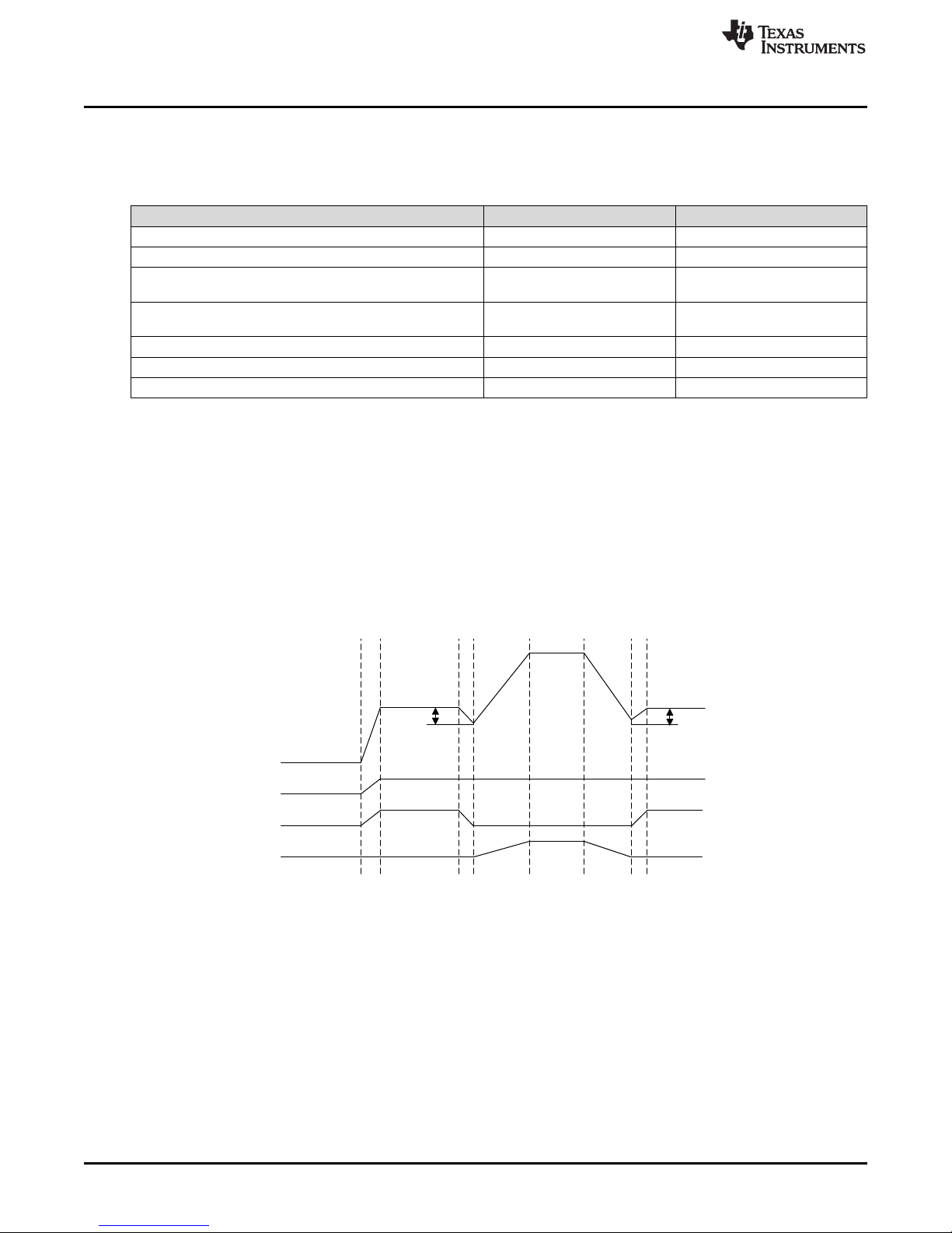
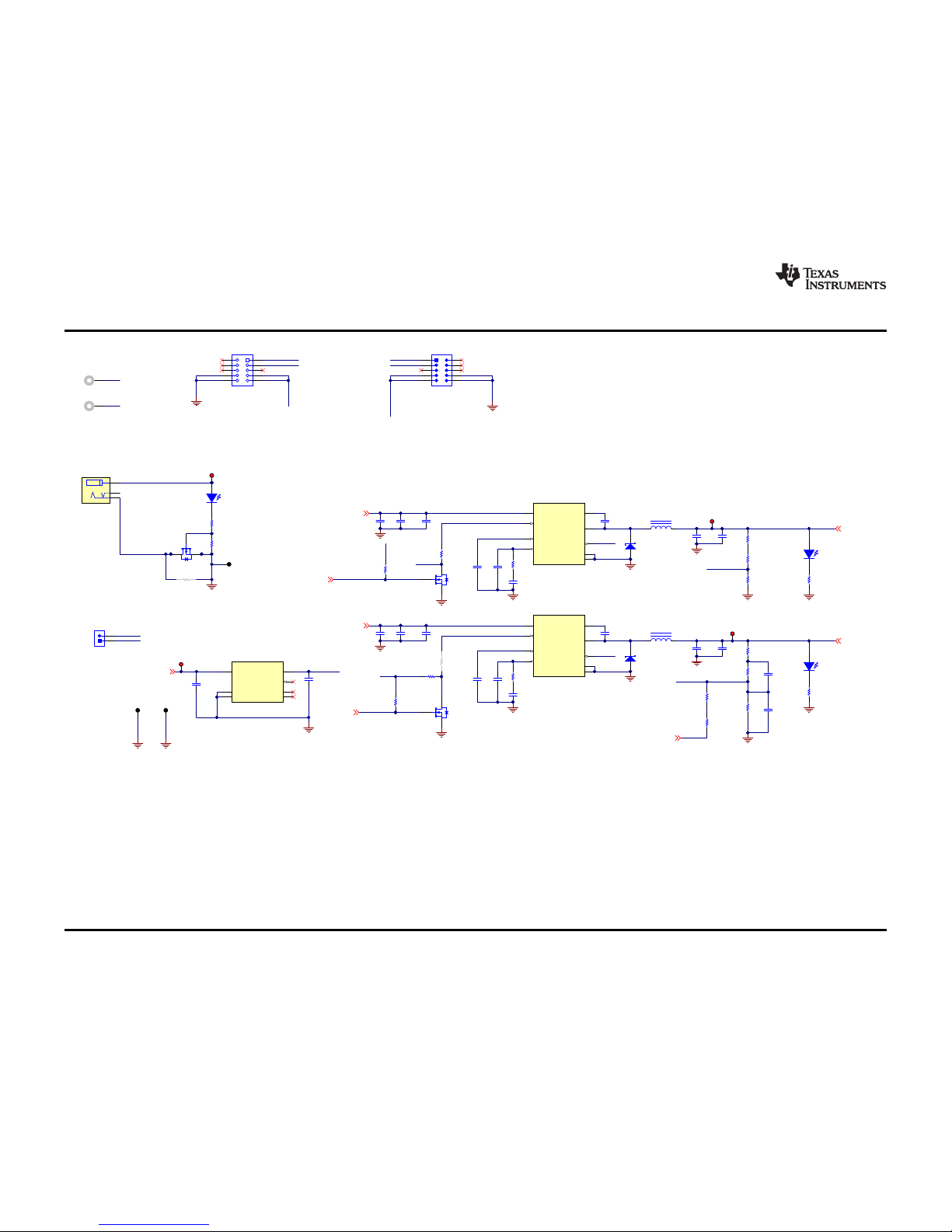
Referring to the schematics in Figure 3 and Figure 4, a 24-V DC input is applied at the J11 terminals or J9
and J13 connectors. There are two DC_DC output nodes, which are regulated by two separate TPS54531
(U1, U4) and associated circuitry.
A USB Type-C UFP is plugged in at J12. When the TPS25741 or TPS25741A detects the UFP via CC1 or
CC2, then Q7 will be turned on by GDNG. If a 5-V contract is established, Q8 will be turned on by G5V, so
5 V will be applied onto the VBUS. If a 12-V contract is established, Q8 is turned off first and then Q3 and
Q4 are turned on by GDPG, so 12 V will be applied onto the VBUS. The voltage request is processed by
the TPS25741 or TPS25741A and then is relayed by gate drivers (GDNG, G5V, GDPG). The relationship
between the VBUS and gate drivers is shown in Figure 2.
Configurable to 5 A
Configurable to 6.3 A
www.ti.com
Default: 3 A
Configurable to 5 A
Default: 4.2 A
Configurable to 6.3 A
Figure 2. Switching Between 5 V and 12 V Using GDNG, G5V, and GDPG
The DC-DC converter can also implement a power saving feature when in unattached status. U4 is not
enabled until a valid UFP is inserted. By using the enable pin of TPS54531, power consumption can be
minimized. To configure U4 as always on, remove R45 and R51 and install R21.
For more information and detailed design information, refer to the TPS25741 and TPS25741A data sheet
(SLVSDJ5).
4
TPS25741EVM-802 and TPS25741AEVM-802 Evaluation Module User
Guide for Desktops
Copyright © 2016–2017, Texas Instruments Incorporated
SLVUAS7A–July 2016–Revised February 2017
Submit Documentation Feedback
Page 5

GND
A1
SSTXP1
A2
SSTXN1
A3
VBUS
A4
CC1
A5
DP1
A6
DN1
A7
RFU1
A8
VBUS
A9
SSRXN2
A10
SSRXP2
A11
GND
A12
GND
B1
SSTXP2
B2
SSTXN2
B3
VBUS
B4
CC2
B5
DP2
B6
DN2
B7
RFU2
B8
VBUS
B9
SSRXN1
B10
SSRXP1
B11
GND
B12
Shield
S1
Shield
S2
Shield
S3
Shield
S4
Shield
S5
Shield
S6
Shield
S7
Shield
S8
J12
898-43-024-90-310000
DP1
1
GND2NC
3
NC
4
IN5DM1
6
U5
TPS2514ADBVR
1 2
3 4
5 6
7 8
J4
1 2
3 4
5 6
7 8
J3
HDVDD
PSEL
PCTRL
HDVDD
PSEL
HIPWR
HDVDD
EN12V
DVDD
HIPWR
HDVDD
PCTRL
HIPWR
PSEL
EN12V
DVDD
/UFP
VBUS
VBUS
7,8
1,2,3
5,6,
Q7
7,8
1,2,3
5,6,
Q8
120
R34
0.005
R44
VBUS
VAUX
VTX
VPWR
VDD
VIN
1.0M
R50
330pF
C15
330pF
C19
CTL2
CTL2
10µF
C37
PGND PGND
40V
D7
TP16
VBUS
CTL1
TP5
CTL1
TP6
CTL2
CTL2CTL1
POL
D4
DEBUG
D3
AUDIO
D2
CC1 CC2
PGND PGND
DN
DP
DN
DP
J14
VBUS
VBUS
DN
DP
TP12
DSCG
DNP
TP15
GDNG
TP14
G5V
TP8
GDP0
J8
PGND
PGND
J16
V_Cable
CTL1
TP7
CC1
TP4
CC2
CC1 CC2
Ra
Rd
J15
BC1.2
0.33µF
C21
0.01µF
C30
PGND
680k
R51
TP9
PFET_S
24
R37
0
R35
VBUS
Q9
PGND
2.2k
R53
Q11 Q10
PGND
PGNDPGND
PGND
PGND
PGND
PGND
PGND
PGND
0
R38
LDO_OUT
10
R46
1.0k
R49
Green
D13
Green
D11
Green
D10
100k
R60
100k
R55
100k
R56
100k
R58
5.1k
R54
8.2k
R62
100VD18
100VD17
100V
D15
J18
V_LED
DCDC_2
DCDC_2
DCDC_5V
DCDC_5V
PGND
VDD
LDO_OUT
DCDC_5V
DCDC_5V
LDO_OUT
510
R19
HDVDD
/UFP
CC1
CC2
10
R26
10
R28
10
R30
Ra
Rd
5.1k
R17
5.1k
R10
1.0k
R11
1.0k
R18
100k
R15
100k
R16
100k
R1
100k
R20
100k
R2
100k
R14
2.2k
R24
2.2k
R23
2.2k
R22
0
R29
0
R32
1
2
3
J5
1
2
3
J6
1
2
3
J10
1
2
3
J7
7,8
1,2,3
5,6,
Q3
7,8
1,2,3
5,6,
Q4
LDO_OUT
Q2
510k
R25
1000pF
C12
PGND
10M
R27
10
R31
TP11
VCONN
DNP
132
NC
5.6V
D16
132
NC
12V
D14
0.012 µF
C24
133k
R39
1200pF
C14
15k
R61
15k
R57
AGND
23
CC1
2
CC2
4
CTL1
7
CTL2
8
DSCG
31
DVDD
18
GD
20
G5V
32
GDNG
29
GDNS
30
GDPG
27
GND
5
HIPWR
6
ISNS
24
NC
11
NC
12
NC
13
PAD
33
PCTRL
19
PSEL
16
VAUX
21
VBUS
26
VCONN
3
VDD
22
VIO
17
VPWR
25
VTX
1
AUDIO
28
DEBUG
15
EN12V
10
POL
9
UFP
14
U3
TPS25741RSM
OP
0.1µF
C26
0.1µF
C27
0.1µF
C18
0.1µF
C32
0.1µF
C17
0.1µF
C25
30V
D6
0.1µF
C34
0
R21
DNP
Copyright © 2016, Texas Instruments Incorporated
or
TPS25741ARSM
www.ti.com
Schematic
5
SLVUAS7A–July 2016 –Revised February 2017
Submit Documentation Feedback
Copyright © 2016–2017, Texas Instruments Incorporated
TPS25741EVM-802 and TPS25741AEVM-802 Evaluation Module User Guide
for Desktops
3 Schematic
Figure 3 and Figure 4 illustrate the EVM schematics.
Figure 3. TPS54531 Buck Power Supply (TPS25741EVM-802 Values Shown)
Page 6
1
3
2
J11
J9
GND_1
J13
VIN
VIN
GND_1
GND_1
VIN
J2
TP13
VIN
DCDC_5V
TP10
PGND
Vin
D9
DCDC_2
VIN
VIN
0.1µF
C33
51
R43
82pF
C22
VSENSE1
VSENSE1
CTL1
CTL1
Q1
CTL2
CTL2
10k
R12
10k
R13
DCDC_5V
LDO_OUT
3300pF
C23
2.2k
R48
8.2k
R47
Vin
Vin_2
1 2
3 4
5 6
7 8
9 10
J1
1
3
56
4
2
7
910
8
J17
PGND
Vin
/UFP
PCTRL
PGNDVin_2
/UFP
PCTRL
Green
D12
2.2k
R59
PGND
Green
D5
5.1k
R36
PGND
PGND
LDO_OUT
TP2
LDO_OUT
TP18
DCDC_5V
TP17
DCDC_2
0.1µF
C31
Vin
LDO_OUT
0.47µF
C11
BOOT
1
VIN
2
EN
3
SS
4
VSENSE
5
COMP
6
GND
7
PH
8
PAD
9
U4
TPS54531DDAR
30k
R40
PGND
10.2k
R42
8.2µH
L2
PGND
PGND
0.01µF
C20
Q5
PGND
/UFP
LDO_OUT
910k
R33
VIN
VIN
0.1µF
C10
51
R9
82pF
C4
VSENSE2
VSENSE2
DCDC_2
3300pF
C1
PGND
PGND
0.1µF
C9
BOOT
1
VIN
2
EN
3
SS
4
VSENSE
5
COMP
6
GND
7
PH
8
PAD
9
U1
TPS54531DDAR
30k
R6
PGND
10.2k
R8
8.2µH
L1
PGND
PGND
0.01µF
C5
732
R7
499
R3
499
R5
0.01µF
C3
0.1µF
C2
22µF
C13
22µF
C16
PGND
PGND
PGND
2.2µF
C6
/UFP
30V
D8
30V
D1
7,8
1,2,3
5,6,
Q6
0
R4
DNP
0
R45
0
R52
DNP
1.87k
R41
Input: 24V
TP3
PGND
PGND
TP1
PGND
PGND
10µF
C28
10µF
C29
10µFC710µF
C8
22µF
C35
22µF
C36
PGND
OUT
1
NC
2
GND
3
EN
4
NC
5
IN
6
PAD
7
U2
TPS70933DRVR
OP
Copyright © 2016, Texas Instruments Incorporated
R8, 7.50k for
TPS25741A
Schematic
www.ti.com
6
SLVUAS7A–July 2016 –Revised February 2017
Submit Documentation Feedback
Copyright © 2016–2017, Texas Instruments Incorporated
TPS25741EVM-802 and TPS25741AEVM-802 Evaluation Module User Guide
for Desktops
Figure 4. TPS25741 (TPS25741EVM-802 Values Shown)
Page 7
www.ti.com
4 Configuring the EVM
4.1 Physical Access
Table 2 lists the TPS25741EVM connector and functionality, Table 3 describes the default jumper
configuration, and Table 4 describes the test point availability.
Connector Label Description
J13 VIN Power bus input. Apply bus input voltage between J13 and J9.
J14 VBUS Output voltage that is applied to the VBUS of the USB Type-C cable. J14 along with J8 can
J9, J8 GND Power bus input return connector
J11 J11 Barrel jack input from an AC to DC power supply
J12 J12 USB Type-C receptacle
D9 VIN This Green LED indicates input power supply
D12, D5 DCDC_5V,
DCDC_2
D2, D3, D4 AUDIO
DEBUG
POL
D13, D11, D10 5 V
9 V/12 V
15 V/20 V
Configuring the EVM
Table 2. Connector and LED Functionality
be used to apply an external load.
The two Green LEDs indicate whether upstream DCDCs are on
D2 indicates when the AUDIO accessary adaptor is inserted
D3 indicates when the DEBUG accessary adaptor is inserted
D4 indicates when the UFP is inserted on positive orientation
D13 indicates when output voltage is 5 V
D11 indicates when output voltage is 9 V or 12 V
D10 indicates when output voltage is 15 V or 20 V
Table 3. Jumper Functionality
Jumper Label Description
J4 PSEL/PCTRL Used to program the PSEL and PCTRL pins of the TPS25741 and TPS25741A. This advertises
J3 HIPWR/ENMV Used to program the HIPWR and EN12V/EN9V pins of the TPS25741 and TPS25741A. This
J16 V_Cable Used to disconnect D2, D3, D4
J18 V_LED Used to disconnect D10, D11, D13
J15 BC 1.2 Used to enable or disable the BC1.2 function
J5 VPWR Used to select power source for VPWR
J6 VPDD Used to select power source for VDD
J10, J7 CC1, CC2 Used to put Ra or Rd to CC lines
J1, J17 Used to connect two EVMs together to enable PPM
J2 Used to enable two EVMs to share a single power supply when doing PPM
the power level to the UFP. Install a single shunt in the P1, P2, P3, or P4 position. Optionally, a
second shunt can be installed in the PCTRL position. The position locations are shown in
Figure 5 and also on the PCB silk screen near J4.
P1 position: PSEL = 93 W
P2 position (default): PSEL = 65 W
P3 position: PSEL = 45 W
P4 position: PSEL = 36 W
PCTRL position (shunt installed): PMAX = PSEL/2
PCTRL position (no shunt installed-default): PMAX = PSEL
advertises maximum voltage and maximum current to the UFP. Install a single shunt in the H1,
H2, H3, or H4 position. Optionally, a second shunt can be installed in the EN12V position. The
position locations are shown in Figure 4 and also on the PCB silk screen near J3. V1 = 5 V, V2 =
9 V or 12 V, V3 = 15 V or 20 V
EN12V or EN9V = HIGH (no shunt installed-default) => V1 and V2
EN12V or EN9V = LOW (shunt installed) => No V2
H1 position: V3 and IMAX = 5 A (OCP = 6.3 A)
H2 position: => V3 and IMAX = 3 A (OCP = 4.2 A)
H3 position: No V3 and IMAX = 5 A (OCP = 6.3 A)
H4 position (default): No V3 and IMAX = 3 A (OCP = 4.2 A)
Advertised current at Vx => Ix = min(PMAX/Vx, IMAX)
SLVUAS7A–July 2016–Revised February 2017
Submit Documentation Feedback
TPS25741EVM-802 and TPS25741AEVM-802 Evaluation Module User
Copyright © 2016–2017, Texas Instruments Incorporated
Guide for Desktops
7
Page 8

DVDD
PCTRL
PSEL
100 kŸ
220 kŸ
VAUX
100 kŸ
PSEL
P1 P2
P3 P4
DVDD
EN12V
or
EN9V
HIPWR
100 kŸ
220 kŸ
DVDD
100 kŸ
HIPWR
H1 H2
H3 H4
J4 J3
Configuring the EVM
J7 J8 Description
TP13 VIN Input voltage
TP18 DCDC_5V Output of the 5 V Buck
TP17 DCDC_2 Output of the higher voltage Buck
TP1/TP3
/TP10
TP7,
TP4
TP8/TP9 GDPG/PFE
TP14/TP15G5V/GDNG NFETs Gate test points
www.ti.com
Table 4. Test Points
GND Output ground test points
CC1, CC2 CC lines test points
PFETs Drain and Source test points
T_S
TP5,
TP6
CTL1, CTL2 Control signals coming from the TPSP25741 and TPS25741A that adjust the output voltage of the buck
boost converter based on the following table:
Voltage Contained in PDO Requested by UFP CTL2 State CTL1 State
5 V High-z High-z
12 V or 9 V Low High-z
20 V or 15 V Low Low
NOTE: DCDC_2 voltage is changed dynamically from V2 to V3 (or V3 to V2)
by CTL1. For V1 to V3 (or V3 to V1) transitions, a momentary pause
at V2 may be observed in the VBUS waveform. To inhibit the
momentary pause at V2, the CTL1 signal may be connected to GND
to default DCDC_2 at the V3 voltage instead of the V2 voltage. For
this configuration, use a jumper wire from TP5 to TP1, TP3, or TP10.
TP11 VCONN VCONN test points
TP16 VBUS Voltage that is applied to the VBUS of the USB Type-C receptacle and cable
4.2 Setting Advertisement Levels with J4 and J3
The advertised power, voltages, and currents can be configured using J4 and J3 as shown in Figure 5.
8
TPS25741EVM-802 and TPS25741AEVM-802 Evaluation Module User
Guide for Desktops
Figure 5. Setting Advertisement Levels with J4 and J3
Copyright © 2016–2017, Texas Instruments Incorporated
SLVUAS7A–July 2016–Revised February 2017
Submit Documentation Feedback
Page 9

www.ti.com
4.3 Equipment Setup
The following is required to set up the equipment:
• Power supply capable of 24 V and preferably 3 A (72 W)
• Resistive or electronic load
• PD-capable UFP to negotiate voltages.
• USB Type-C cable
5 Operation
Use the following steps to operate the EVM:
• Turn on the input power supply to 24 V.
• Connect the UFP to the TPS25741 or TPS25741A EVM through a USB Type-C cable.
• Make desired voltage requests from the UFP to TPS25741 or TPS25741A EVM.
• Connect load between J8 and J14 as desired to test features and other performance.
6 Test Results
This section provides typical performance waveforms for the TPS25741EVM-802 and TPS25741AEVM802 with VIN= 24 V at different load conditions. Actual performance data is affected by measurement
techniques and environmental variables; therefore, these curves are presented for reference and may
differ from actual results obtained.
Configuring the EVM
Figure 6. Mux Between 5 V and 12 V at No Load Figure 7. Mux Between 5 V and 12 V at 3 A
Figure 8. Mux Between 5 V and 20 V at No Load Figure 9. Mux Between 5 V and 20 V at 3 A
SLVUAS7A–July 2016–Revised February 2017
Submit Documentation Feedback
TPS25741EVM-802 and TPS25741AEVM-802 Evaluation Module User
Copyright © 2016–2017, Texas Instruments Incorporated
Guide for Desktops
9
Page 10

Test Results
www.ti.com
Figure 10. 5-V to 12-V Transition Figure 11. 5-V to 20-V Transition
Figure 12. Start Into Short on Output Figure 13. Hot Short on Output 5 V
Figure 14. Hot Short on Output 12 V Figure 15. Hot Short on Output 20 V
Figure 16. Load Step From 0 A to 3 A (12 V) Figure 17. Load Step From 0 A to 3 A (20 V)
10
TPS25741EVM-802 and TPS25741AEVM-802 Evaluation Module User
Guide for Desktops
SLVUAS7A–July 2016–Revised February 2017
Copyright © 2016–2017, Texas Instruments Incorporated
Submit Documentation Feedback
Page 11

www.ti.com
Test Results
Figure 18. 5.5-A Load Step Triggers OCP (5 V) Figure 19. 5.5-A Load Step Triggers OCP (12 V)
Figure 20. 5.5-A Load Step Triggers OCP (20 V)
Figure 22. VCONN With 200-mA Load Figure 23. VCONN OCP
spacerOne port for MacBook®, the other for legacy smart-phone.
Figure 21. Port Power Management
SLVUAS7A–July 2016–Revised February 2017
Submit Documentation Feedback
TPS25741EVM-802 and TPS25741AEVM-802 Evaluation Module User
Copyright © 2016–2017, Texas Instruments Incorporated
Guide for Desktops
11
Page 12

Copyright © 2016, Texas Instruments Incorporated
Copyright © 2016, Texas Instruments Incorporated
Board Layout Image
7 Board Layout Image
Figure 24 through Figure 28 illustrate the top layer assembly drawing and PCB layout images.
www.ti.com
Figure 24. Top Layer Assembly
12
TPS25741EVM-802 and TPS25741AEVM-802 Evaluation Module User
Guide for Desktops
Figure 25. Top Layer
SLVUAS7A–July 2016–Revised February 2017
Copyright © 2016–2017, Texas Instruments Incorporated
Submit Documentation Feedback
Page 13

Copyright © 2016, Texas Instruments Incorporated
Copyright © 2016, Texas Instruments Incorporated
www.ti.com
Board Layout Image
Figure 26. Signal Layer 1
SLVUAS7A–July 2016–Revised February 2017
Submit Documentation Feedback
Figure 27. Signal Layer 2
TPS25741EVM-802 and TPS25741AEVM-802 Evaluation Module User
Copyright © 2016–2017, Texas Instruments Incorporated
Guide for Desktops
13
Page 14

Copyright © 2016, Texas Instruments Incorporated
Board Layout Image
www.ti.com
Figure 28. Bottom Layer
14
TPS25741EVM-802 and TPS25741AEVM-802 Evaluation Module User
Guide for Desktops
SLVUAS7A–July 2016–Revised February 2017
Copyright © 2016–2017, Texas Instruments Incorporated
Submit Documentation Feedback
Page 15

www.ti.com
Bill of Materials
15
SLVUAS7A–July 2016 –Revised February 2017
Submit Documentation Feedback
Copyright © 2016–2017, Texas Instruments Incorporated
TPS25741EVM-802 and TPS25741AEVM-802 Evaluation Module User Guide
for Desktops
8 Bill of Materials
Table 5 lists the EVM BOM.
Table 5. Bill of Materials
Designator Qty Value Description Package Reference Part Number Manufacturer Alternate Part
Number
Alternate
Manufacturer
!PCB 1 Printed Circuit Board PWR802 Any - C1, C23 2 3300pF CAP, CERM, 3300 pF, 50 V, +/- 10%, X7R, 0603 0603 C0603C332K5RACTU Kemet
C2 1 0.1uF CAP, CERM, 0.1 µF, 25 V, +/- 5%, X7R, 0603 0603 06033C104JAT2A AVX
C3, C5, C20 3 0.01uF CAP, CERM, 0.01 µF, 25 V, +/- 5%, C0G/NP0, 0603 0603 C0603H103J3GACTU Kemet
C4, C22 2 82pF CAP, CERM, 82 pF, 50 V, +/- 5%, C0G/NP0, 0603 0603 06035A820JAT2A AVX
C6 1 2.2uF CAP, CERM, 2.2 µF, 16 V, +/- 10%, X5R, 0805 0805 0805YD225KAT2A AVX
C7, C8, C28, C29 4 10uF CAP, CERM, 10 µF, 50 V, +/- 10%, X5R, 1206 1206 C3216X5R1H106K160AB TDK
C9, C31 2 0.1uF CAP, CERM, 0.1 µF, 50 V, +/- 10%, X7R, 0603 0603 885012206095 WurthElektronik
C10, C33 2 0.1uF CAP, CERM, 0.1 µF, 16 V, +/- 10%, X5R, 0402 0402 GRM155R61C104KA88D Murata
C11 1 0.47uF CAP,CERM, 0.47 µF, 50 V, +/- 10%, X7R, 0805 0805 UMK212B7474KG-T Taiyo Yuden
C12 1 1000pF CAP, CERM, 1000 pF, 50 V, +/- 10%, X7R, 0603 0603 C0603C102K5RACTU Kemet
C13, C16, C35, C36 4 22uF CAP, CERM, 22 µF, 25 V, +/- 20%, X5R, 1210 1210 12103D226MAT2A AVX
C14 1 1200pF CAP, CERM, 1200 pF, 50 V, +/- 10%, X7R, 0603 0603 GRM188R71H122KA01D Murata
C15, C19 2 330pF CAP, CERM, 330 pF, 50 V, +/- 5%, C0G/NP0, 0603 0603 06035A331JAT2A AVX
C17, C18, C25,
C26, C27, C32, C34
7 0.1uF CAP, CERM, 0.1 µF, 50 V, +/- 10%, X7R, 0402 0402 C1005X7R1H104K050BB TDK
C21 1 0.33uF CAP,CERM, 0.33 µF, 25 V, +80/-20%, Y5V, 0603 0603 C0603C334Z3VACTU Kemet
C24 1 0.012uF CAP, CERM, 0.012 µF, 50 V, +/- 10%, X7R, 0805 0805 08055C123KAT2A AVX
C30 1 0.01uF CAP,CERM, 0.01 µF, 50 V, +/- 5%, X7R, 0603 0603 C0603C103J5RACTU Kemet
C37 1 10uF CAP, CERM, 10 µF, 25 V, +/- 10%, X7R, 1210 1210 12103C106KAT2A AVX
D1, D8 2 30V Diode, Schottky, 30 V, 5 A, SMA SMA RB080L-30TE25 Rohm
D2 1 AUDIO LED,Green, SMD LED_0603 150060GS75000 Wurth Elektronik
D3 1 DEBUG LED, Green, SMD LED_0603 150060GS75000 Wurth Elektronik
D4 1 POL LED, Green, SMD LED_0603 150060GS75000 Wurth Elektronik
D5, D10, D11, D12,
D13
5 Green LED, Green, SMD LED_0603 150060GS75000 Wurth Elektronik
D6 1 30V Diode, Schottky, 30 V, 0.8 A, SOD-323 SOD-323 CUS08F30,H3F Toshiba
D7 1 40V Diode, Schottky, 40 V, 3 A, SMA SMA B340A-13-F Diodes Inc.
D9 1 Vin LED, Green, SMD LED_0603 150060GS75000 Wurth Elektronik
D14 1 12V Diode, Zener, 12 V, 225 mW, SOT-23 SOT-23 BZX84C12LT1G ON Semiconductor
D15, D17, D18 3 100V Diode, Ultrafast, 100 V, 0.15 A, SOD-123 SOD-123 1N4148W-7-F DiodesInc.
D16 1 5.6V Diode, Zener, 5.6 V, 225 mW, SOT-23 SOT-23 BZX84B5V6LT1G ON Semiconductor
H1, H2, H3, H4 4 MachineScrew, Round, #4-40 x 1/4, Nylon, Philips panhead Screw NY PMS 440 0025 PH B&F Fastener
Supply
H5, H6, H7, H8 4 Standoff,Hex, 0.5"L #4-40 Nylon Standoff 1902C Keystone - J1 1 Header, 2.54mm, 5x2, Gold, R/A, TH Header, 2.54mm, 5x2,
R/A, TH
61301021021 WurthElektronik
Page 16

Bill of Materials
www.ti.com
16
SLVUAS7A–July 2016 –Revised February 2017
Submit Documentation Feedback
Copyright © 2016–2017, Texas Instruments Incorporated
TPS25741EVM-802 and TPS25741AEVM-802 Evaluation Module User Guide
for Desktops
Table 5. Bill of Materials (continued)
Designator Qty Value Description Package Reference Part Number Manufacturer Alternate Part
Number
Alternate
Manufacturer
J2, J15, J16, J18 4 Header, 100mil, 2x1, Tin, TH Header, 2x1, 100mil,TH5-146278-2 TE Connectivity
J3, J4 2 Header, 2.54mm, 4x2, Gold, SMT Header, 2.54mm, 4x2,
SMT
TSM-104-01-L-DV Samtec
J5, J6, J7, J10 4 Header, 100mil, 3x1, Gold, TH 3x1 Header TSW-103-07-G-S Samtec
J8, J9, J13, J14 4 Standard Banana Jack, Uninsulated, 5.5mm Keystone_575-4 575-4 Keystone
J11 1 Connector, DC Jack 2.1X5.5 mm, TH Conn, DC Jack, pin
2mm Dia.
PJ-202AH CUI Inc.
J12 1 Connector, Receptacle, USB Type-C, R/A, TH Connector,
Receptacle, USB
Type-C, R/A, TH
898-43-024-90-310000 Mill-Max
J17 1 Connector, Receptacle, 100mil, 5x2, Gold plated, R/A, TH 5x2 R/A Header
Receptacle
PPPC052LJBN-RC Sullins Connector
Solutions
L1, L2 2 8.2uH Inductor, Shielded Drum Core, Ferrite, 8.2uH, 6.25A, 0.014
ohm, SMD
WE-PD-L 744771008 Wurth Elektronik
eiSos
LBL1 1 Thermal Transfer Printable Labels, 0.650" W x 0.200" H -
10,000 per roll
PCB Label 0.650"H x
0.200"W
THT-14-423-10 Brady - -
Q1, Q5, Q9, Q10,
Q11
5 60V MOSFET,N-CH, 60 V, 0.17 A, SOT-23 SOT-23 2N7002-7-F Diodes Inc. None
Q2 1 -60V MOSFET, P-CH, -60 V, -0.3 A, SOT-23 SOT-23 BSH201,215 NXP Semiconductor None
Q3, Q4 2 -30V MOSFET, P-CH, -30 V, -35 A, PowerPAK 1212 PowerPAK 1212 SI7625DN-T1-GE3 Vishay-Siliconix None
Q6, Q7, Q8 3 30V MOSFET, N-CH, 30 V, 20 A, SON 3.3x3.3mm SON 3.3x3.3mm CSD17579Q3A Texas Instruments None
R1, R2, R14, R15,
R16, R20
6 100k RES, 100 k, 0.5%, 0.063 W, 0402 0402 CRCW0402100KDHEDP Vishay-Dale
R3, R5 2 499 RES, 499, 1%, 0.1 W, 0603 0603 CRCW0603499RFKEA Vishay-Dale
R6, R40 2 30k RES, 30 k, 5%, 0.1 W, 0603 0603 CRCW060330K0JNEA Vishay-Dale
R7 1 732 RES, 732, 1%, 0.1 W, 0603 0603 CRCW0603732RFKEA Vishay-Dale
R8, R42 2 10.2k RES, 10.2 k, 1%, 0.1 W, 0603 0603 CRCW060310K2FKEA Vishay-Dale
R9, R43 2 51 RES, 51, 5%, 0.1 W, 0603 0603 CRCW060351R0JNEA Vishay-Dale
R10, R17 2 5.1k RES, 5.1 k, 5%, 0.063 W, 0402 0402 CRCW04025K10JNED Vishay-Dale
R11, R18 2 1.0k RES, 1.0 k, 5%, 0.063 W, 0402 0402 CRCW04021K00JNED Vishay-Dale
R12, R13 2 10k RES, 10 k, 5%, 0.1 W, AEC-Q200 Grade 0, 0402 0402 ERJ-2GEJ103X Panasonic
R19 1 510 RES, 510, 5%, 0.1 W, 0603 0603 CRCW0603510RJNEA Vishay-Dale
R22, R23, R24 3 2.2k RES, 2.2 k, 5%, 0.063 W, 0402 0402 CRCW04022K20JNED Vishay-Dale
R25 1 510k RES, 510 k, 5%, 0.1 W, 0603 0603 CRCW0603510KJNEA Vishay-Dale
R26, R28, R30,
R31, R46
5 10 RES, 10, 5%, 0.25 W, 0603 0603 CRCW060310R0JNEAHP Vishay-Dale
R27 1 10Meg RES, 10 M, 5%, 0.1 W, 0603 0603 CRCW060310M0JNEA Vishay-Dale
R29, R32, R35,
R38, R45
5 0 RES, 0, 5%, 0.063 W, 0402 0402 ERJ-2GE0R00X Panasonic
R33 1 910k RES, 910 k, 5%, 0.1 W, 0603 0603 CRCW0603910KJNEA Vishay-Dale
R34 1 120 RES, 120 ohm, 5%, 0.25W, 1206 1206 CRCW1206120RJNEA Vishay-Dale
R36, R54 2 5.1k RES, 5.1 k, 5%, 0.1 W, 0603 0603 CRCW06035K10JNEA Vishay-Dale
R37 1 24 RES, 24, 5%, 0.063 W, 0402 0402 CRCW040224R0JNED Vishay-Dale
Page 17

www.ti.com
Bill of Materials
17
SLVUAS7A–July 2016 –Revised February 2017
Submit Documentation Feedback
Copyright © 2016–2017, Texas Instruments Incorporated
TPS25741EVM-802 and TPS25741AEVM-802 Evaluation Module User Guide
for Desktops
Table 5. Bill of Materials (continued)
Designator Qty Value Description Package Reference Part Number Manufacturer Alternate Part
Number
Alternate
Manufacturer
R39 1 133k RES, 133 k, 1%, 0.1 W, 0603 0603 CRCW0603133KFKEA Vishay-Dale
R41 1 1.87k RES, 1.87 k, 1%, 0.1 W, 0603 0603 CRCW06031K87FKEA Vishay-Dale
R44 1 0.005 RES, 0.005, 1%, 0.5 W, 1206 1206 WSL12065L000FEA18 Vishay-Dale
R47, R62 2 8.2k RES, 8.2 k, 5%, 0.1 W, 0603 0603 RC0603JR-078K2L Yageo America
R48, R53, R59 3 2.2k RES, 2.2 k, 5%, 0.1 W, 0603 0603 RC0603JR-072K2L Yageo America
R49 1 1.0k RES,1.0 k, 5%, 0.1 W, 0603 0603 CRCW06031K00JNEA Vishay-Dale
R50 1 1.0Meg RES, 1.0 M, 5%, 0.1 W, 0603 0603 CRCW06031M00JNEA Vishay-Dale
R51 1 680k RES, 680 k, 5%, 0.1 W, 0603 0603 CRCW0603680KJNEA Vishay-Dale
R55, R56, R58, R60 4 100k RES, 100 k, 5%, 0.1 W, 0603 0603 CRCW0603100KJNEA Vishay-Dale
R57, R61 2 15k RES, 15 k, 5%, 0.1 W, 0603 0603 CRCW060315K0JNEA Vishay-Dale
SH-J1, SH-J2, SH-
J3, SH-J4, SH-J5,
SH-J6, SH-J7, SHJ8
8 1x2 Shunt, 100mil, Gold plated, Black Shunt 969102-0000-DA 3M SNT-100-BK-G Samtec
TP1, TP3, TP10 3 Black Test Point, Miniature, Black, TH Black Miniature
Testpoint
5001 Keystone
TP2, TP13, TP16,
TP17, TP18
5 Red Test Point, TH, Miniature, Red Keystone5000 5000 Keystone - -
TP4, TP5, TP6,
TP7, TP8, TP9,
TP14, TP15
8 White Test Point, Miniature, White, TH White Miniature
Testpoint
5002 Keystone
U1, U4 2 5-A, 28-V Input, Step-Down SWIFT™ DC-DC Converter With
Eco-mode™, DDA0008E
DDA0008E TPS54531DDAR Texas Instruments TPS54531DDA Texas Instruments
U2 1 150-mA, 3.3-V, 1-µA IQ Voltage Regulators with Enable,
DRV0006A
DRV0006A TPS70933DRVR Texas Instruments TPS70933DRVT Texas Instruments
U3 1 USB PD Baseband and USB Type-C Power Controller,
RSM0032B
RSM0032B TPS25741RSM Texas Instruments Texas Instruments
U5 1 USB Dedicated Charging Port Controller, DBV0006A DBV0006A TPS2514ADBVR Texas Instruments TPS2514ADBVT Texas Instruments
FID1, FID2, FID3 0 Fiducial mark. There is nothing to buy or mount. Fiducial N/A N/A
R4, R21, R52 0 0 RES, 0, 5%, 0.063 W, 0402 0402 ERJ-2GE0R00X Panasonic
TP11 0 Red Test Point, TH, Miniature, Red Keystone5000 5000 Keystone - TP12 0 White Test Point, Miniature, White, TH White Miniature
Testpoint
5002 Keystone
Notes: Unless otherwise noted in the Alternate Part Number or Alternate Manufacturer columns, all parts may be substituted with equivalents.
Page 18

Revision History
www.ti.com
Revision History
NOTE: Page numbers for previous revisions may differ from page numbers in the current version.
Changes from Original (July 2016) to A Revision ........................................................................................................... Page
• Reversed the voltages in the two Buck blocks and changed the device name to TPS2514A in the TPS25741EVM Block
Diagram..................................................................................................................................... 3
• Changed Output Voltages and Advertised Voltages in the TPS25741AEVM-802 column from 5 V, 12 V, 20 V to 5 V, 9 V,
15 V of the TPS25741 and TPS25741A EVM Electrical and Performance Specifications at 25°C table...................... 4
• Changed value on C24 to 0.012 from 0.027 µF in the TPS54531 Buck Power Supply schematic............................. 5
• Changed the Description column of the J3 row in the Jumper Functionality table. .............................................. 7
• Added a NOTE to the TP5, TP6 row in the Description column of the Test Points table........................................ 8
• Changed the capacitor values in the C24 row to 0.012 µF from 0.027 µF, and changed the Part Number to
08055C123KAT2A in the BOM. ....................................................................................................... 15
18
Revision History
SLVUAS7A–July 2016–Revised February 2017
Copyright © 2016–2017, Texas Instruments Incorporated
Submit Documentation Feedback
Page 19

STANDARD TERMS FOR EVALUATION MODULES
1. Delivery: TI delivers TI evaluation boards, kits, or modules, including any accompanying demonstration software, components, and/or
documentation which may be provided together or separately (collectively, an “EVM” or “EVMs”) to the User (“User”) in accordance
with the terms set forth herein. User's acceptance of the EVM is expressly subject to the following terms.
1.1 EVMs are intended solely for product or software developers for use in a research and development setting to facilitate feasibility
evaluation, experimentation, or scientific analysis of TI semiconductors products. EVMs have no direct function and are not
finished products. EVMs shall not be directly or indirectly assembled as a part or subassembly in any finished product. For
clarification, any software or software tools provided with the EVM (“Software”) shall not be subject to the terms and conditions
set forth herein but rather shall be subject to the applicable terms that accompany such Software
1.2 EVMs are not intended for consumer or household use. EVMs may not be sold, sublicensed, leased, rented, loaned, assigned,
or otherwise distributed for commercial purposes by Users, in whole or in part, or used in any finished product or production
system.
2 Limited Warranty and Related Remedies/Disclaimers:
2.1 These terms do not apply to Software. The warranty, if any, for Software is covered in the applicable Software License
Agreement.
2.2 TI warrants that the TI EVM will conform to TI's published specifications for ninety (90) days after the date TI delivers such EVM
to User. Notwithstanding the foregoing, TI shall not be liable for a nonconforming EVM if (a) the nonconformity was caused by
neglect, misuse or mistreatment by an entity other than TI, including improper installation or testing, or for any EVMs that have
been altered or modified in any way by an entity other than TI, (b) the nonconformity resulted from User's design, specifications
or instructions for such EVMs or improper system design, or (c) User has not paid on time. Testing and other quality control
techniques are used to the extent TI deems necessary. TI does not test all parameters of each EVM.
User's claims against TI under this Section 2 are void if User fails to notify TI of any apparent defects in the EVMs within ten (10)
business days after delivery, or of any hidden defects with ten (10) business days after the defect has been detected.
2.3 TI's sole liability shall be at its option to repair or replace EVMs that fail to conform to the warranty set forth above, or credit
User's account for such EVM. TI's liability under this warranty shall be limited to EVMs that are returned during the warranty
period to the address designated by TI and that are determined by TI not to conform to such warranty. If TI elects to repair or
replace such EVM, TI shall have a reasonable time to repair such EVM or provide replacements. Repaired EVMs shall be
warranted for the remainder of the original warranty period. Replaced EVMs shall be warranted for a new full ninety (90) day
warranty period.
3 Regulatory Notices:
3.1 United States
3.1.1 Notice applicable to EVMs not FCC-Approved:
FCC NOTICE: This kit is designed to allow product developers to evaluate electronic components, circuitry, or software
associated with the kit to determine whether to incorporate such items in a finished product and software developers to write
software applications for use with the end product. This kit is not a finished product and when assembled may not be resold or
otherwise marketed unless all required FCC equipment authorizations are first obtained. Operation is subject to the condition
that this product not cause harmful interference to licensed radio stations and that this product accept harmful interference.
Unless the assembled kit is designed to operate under part 15, part 18 or part 95 of this chapter, the operator of the kit must
operate under the authority of an FCC license holder or must secure an experimental authorization under part 5 of this chapter.
3.1.2 For EVMs annotated as FCC – FEDERAL COMMUNICATIONS COMMISSION Part 15 Compliant:
CAUTION
This device complies with part 15 of the FCC Rules. Operation is subject to the following two conditions: (1) This device may not
cause harmful interference, and (2) this device must accept any interference received, including interference that may cause
undesired operation.
Changes or modifications not expressly approved by the party responsible for compliance could void the user's authority to
operate the equipment.
FCC Interference Statement for Class A EVM devices
NOTE: This equipment has been tested and found to comply with the limits for a Class A digital device, pursuant to part 15 of
the FCC Rules. These limits are designed to provide reasonable protection against harmful interference when the equipment is
operated in a commercial environment. This equipment generates, uses, and can radiate radio frequency energy and, if not
installed and used in accordance with the instruction manual, may cause harmful interference to radio communications.
Operation of this equipment in a residential area is likely to cause harmful interference in which case the user will be required to
correct the interference at his own expense.
Page 20

FCC Interference Statement for Class B EVM devices
NOTE: This equipment has been tested and found to comply with the limits for a Class B digital device, pursuant to part 15 of
the FCC Rules. These limits are designed to provide reasonable protection against harmful interference in a residential
installation. This equipment generates, uses and can radiate radio frequency energy and, if not installed and used in accordance
with the instructions, may cause harmful interference to radio communications. However, there is no guarantee that interference
will not occur in a particular installation. If this equipment does cause harmful interference to radio or television reception, which
can be determined by turning the equipment off and on, the user is encouraged to try to correct the interference by one or more
of the following measures:
• Reorient or relocate the receiving antenna.
• Increase the separation between the equipment and receiver.
• Connect the equipment into an outlet on a circuit different from that to which the receiver is connected.
• Consult the dealer or an experienced radio/TV technician for help.
3.2 Canada
3.2.1 For EVMs issued with an Industry Canada Certificate of Conformance to RSS-210
Concerning EVMs Including Radio Transmitters:
This device complies with Industry Canada license-exempt RSS standard(s). Operation is subject to the following two conditions:
(1) this device may not cause interference, and (2) this device must accept any interference, including interference that may
cause undesired operation of the device.
Concernant les EVMs avec appareils radio:
Le présent appareil est conforme aux CNR d'Industrie Canada applicables aux appareils radio exempts de licence. L'exploitation
est autorisée aux deux conditions suivantes: (1) l'appareil ne doit pas produire de brouillage, et (2) l'utilisateur de l'appareil doit
accepter tout brouillage radioélectrique subi, même si le brouillage est susceptible d'en compromettre le fonctionnement.
Concerning EVMs Including Detachable Antennas:
Under Industry Canada regulations, this radio transmitter may only operate using an antenna of a type and maximum (or lesser)
gain approved for the transmitter by Industry Canada. To reduce potential radio interference to other users, the antenna type
and its gain should be so chosen that the equivalent isotropically radiated power (e.i.r.p.) is not more than that necessary for
successful communication. This radio transmitter has been approved by Industry Canada to operate with the antenna types
listed in the user guide with the maximum permissible gain and required antenna impedance for each antenna type indicated.
Antenna types not included in this list, having a gain greater than the maximum gain indicated for that type, are strictly prohibited
for use with this device.
Concernant les EVMs avec antennes détachables
Conformément à la réglementation d'Industrie Canada, le présent émetteur radio peut fonctionner avec une antenne d'un type et
d'un gain maximal (ou inférieur) approuvé pour l'émetteur par Industrie Canada. Dans le but de réduire les risques de brouillage
radioélectrique à l'intention des autres utilisateurs, il faut choisir le type d'antenne et son gain de sorte que la puissance isotrope
rayonnée équivalente (p.i.r.e.) ne dépasse pas l'intensité nécessaire à l'établissement d'une communication satisfaisante. Le
présent émetteur radio a été approuvé par Industrie Canada pour fonctionner avec les types d'antenne énumérés dans le
manuel d’usage et ayant un gain admissible maximal et l'impédance requise pour chaque type d'antenne. Les types d'antenne
non inclus dans cette liste, ou dont le gain est supérieur au gain maximal indiqué, sont strictement interdits pour l'exploitation de
l'émetteur
3.3 Japan
3.3.1 Notice for EVMs delivered in Japan: Please see http://www.tij.co.jp/lsds/ti_ja/general/eStore/notice_01.page 日本国内に
輸入される評価用キット、ボードについては、次のところをご覧ください。
http://www.tij.co.jp/lsds/ti_ja/general/eStore/notice_01.page
3.3.2 Notice for Users of EVMs Considered “Radio Frequency Products” in Japan: EVMs entering Japan may not be certified
by TI as conforming to Technical Regulations of Radio Law of Japan.
If User uses EVMs in Japan, not certified to Technical Regulations of Radio Law of Japan, User is required to follow the
instructions set forth by Radio Law of Japan, which includes, but is not limited to, the instructions below with respect to EVMs
(which for the avoidance of doubt are stated strictly for convenience and should be verified by User):
1. Use EVMs in a shielded room or any other test facility as defined in the notification #173 issued by Ministry of Internal
Affairs and Communications on March 28, 2006, based on Sub-section 1.1 of Article 6 of the Ministry’s Rule for
Enforcement of Radio Law of Japan,
2. Use EVMs only after User obtains the license of Test Radio Station as provided in Radio Law of Japan with respect to
EVMs, or
3. Use of EVMs only after User obtains the Technical Regulations Conformity Certification as provided in Radio Law of Japan
with respect to EVMs. Also, do not transfer EVMs, unless User gives the same notice above to the transferee. Please note
that if User does not follow the instructions above, User will be subject to penalties of Radio Law of Japan.
Page 21

【無線電波を送信する製品の開発キットをお使いになる際の注意事項】 開発キットの中には技術基準適合証明を受けて
いないものがあります。 技術適合証明を受けていないもののご使用に際しては、電波法遵守のため、以下のいずれかの
措置を取っていただく必要がありますのでご注意ください。
1. 電波法施行規則第6条第1項第1号に基づく平成18年3月28日総務省告示第173号で定められた電波暗室等の試験設備でご使用
いただく。
2. 実験局の免許を取得後ご使用いただく。
3. 技術基準適合証明を取得後ご使用いただく。
なお、本製品は、上記の「ご使用にあたっての注意」を譲渡先、移転先に通知しない限り、譲渡、移転できないものとします。
上記を遵守頂けない場合は、電波法の罰則が適用される可能性があることをご留意ください。 日本テキサス・イ
ンスツルメンツ株式会社
東京都新宿区西新宿6丁目24番1号
西新宿三井ビル
3.3.3 Notice for EVMs for Power Line Communication: Please see http://www.tij.co.jp/lsds/ti_ja/general/eStore/notice_02.page
電力線搬送波通信についての開発キットをお使いになる際の注意事項については、次のところをご覧ください。http:/
/www.tij.co.jp/lsds/ti_ja/general/eStore/notice_02.page
3.4 European Union
3.4.1 For EVMs subject to EU Directive 2014/30/EU (Electromagnetic Compatibility Directive):
This is a class A product intended for use in environments other than domestic environments that are connected to a
low-voltage power-supply network that supplies buildings used for domestic purposes. In a domestic environment this
product may cause radio interference in which case the user may be required to take adequate measures.
4 EVM Use Restrictions and Warnings:
4.1 EVMS ARE NOT FOR USE IN FUNCTIONAL SAFETY AND/OR SAFETY CRITICAL EVALUATIONS, INCLUDING BUT NOT
LIMITED TO EVALUATIONS OF LIFE SUPPORT APPLICATIONS.
4.2 User must read and apply the user guide and other available documentation provided by TI regarding the EVM prior to handling
or using the EVM, including without limitation any warning or restriction notices. The notices contain important safety information
related to, for example, temperatures and voltages.
4.3 Safety-Related Warnings and Restrictions:
4.3.1 User shall operate the EVM within TI’s recommended specifications and environmental considerations stated in the user
guide, other available documentation provided by TI, and any other applicable requirements and employ reasonable and
customary safeguards. Exceeding the specified performance ratings and specifications (including but not limited to input
and output voltage, current, power, and environmental ranges) for the EVM may cause personal injury or death, or
property damage. If there are questions concerning performance ratings and specifications, User should contact a TI
field representative prior to connecting interface electronics including input power and intended loads. Any loads applied
outside of the specified output range may also result in unintended and/or inaccurate operation and/or possible
permanent damage to the EVM and/or interface electronics. Please consult the EVM user guide prior to connecting any
load to the EVM output. If there is uncertainty as to the load specification, please contact a TI field representative.
During normal operation, even with the inputs and outputs kept within the specified allowable ranges, some circuit
components may have elevated case temperatures. These components include but are not limited to linear regulators,
switching transistors, pass transistors, current sense resistors, and heat sinks, which can be identified using the
information in the associated documentation. When working with the EVM, please be aware that the EVM may become
very warm.
4.3.2 EVMs are intended solely for use by technically qualified, professional electronics experts who are familiar with the
dangers and application risks associated with handling electrical mechanical components, systems, and subsystems.
User assumes all responsibility and liability for proper and safe handling and use of the EVM by User or its employees,
affiliates, contractors or designees. User assumes all responsibility and liability to ensure that any interfaces (electronic
and/or mechanical) between the EVM and any human body are designed with suitable isolation and means to safely
limit accessible leakage currents to minimize the risk of electrical shock hazard. User assumes all responsibility and
liability for any improper or unsafe handling or use of the EVM by User or its employees, affiliates, contractors or
designees.
4.4 User assumes all responsibility and liability to determine whether the EVM is subject to any applicable international, federal,
state, or local laws and regulations related to User’s handling and use of the EVM and, if applicable, User assumes all
responsibility and liability for compliance in all respects with such laws and regulations. User assumes all responsibility and
liability for proper disposal and recycling of the EVM consistent with all applicable international, federal, state, and local
requirements.
5. Accuracy of Information: To the extent TI provides information on the availability and function of EVMs, TI attempts to be as accurate
as possible. However, TI does not warrant the accuracy of EVM descriptions, EVM availability or other information on its websites as
accurate, complete, reliable, current, or error-free.
Page 22

6. Disclaimers:
6.1 EXCEPT AS SET FORTH ABOVE, EVMS AND ANY MATERIALS PROVIDED WITH THE EVM (INCLUDING, BUT NOT
LIMITED TO, REFERENCE DESIGNS AND THE DESIGN OF THE EVM ITSELF) ARE PROVIDED "AS IS" AND "WITH ALL
FAULTS." TI DISCLAIMS ALL OTHER WARRANTIES, EXPRESS OR IMPLIED, REGARDING SUCH ITEMS, INCLUDING BUT
NOT LIMITED TO ANY EPIDEMIC FAILURE WARRANTY OR IMPLIED WARRANTIES OF MERCHANTABILITY OR FITNESS
FOR A PARTICULAR PURPOSE OR NON-INFRINGEMENT OF ANY THIRD PARTY PATENTS, COPYRIGHTS, TRADE
SECRETS OR OTHER INTELLECTUAL PROPERTY RIGHTS.
6.2 EXCEPT FOR THE LIMITED RIGHT TO USE THE EVM SET FORTH HEREIN, NOTHING IN THESE TERMS SHALL BE
CONSTRUED AS GRANTING OR CONFERRING ANY RIGHTS BY LICENSE, PATENT, OR ANY OTHER INDUSTRIAL OR
INTELLECTUAL PROPERTY RIGHT OF TI, ITS SUPPLIERS/LICENSORS OR ANY OTHER THIRD PARTY, TO USE THE
EVM IN ANY FINISHED END-USER OR READY-TO-USE FINAL PRODUCT, OR FOR ANY INVENTION, DISCOVERY OR
IMPROVEMENT, REGARDLESS OF WHEN MADE, CONCEIVED OR ACQUIRED.
7. USER'S INDEMNITY OBLIGATIONS AND REPRESENTATIONS. USER WILL DEFEND, INDEMNIFY AND HOLD TI, ITS
LICENSORS AND THEIR REPRESENTATIVES HARMLESS FROM AND AGAINST ANY AND ALL CLAIMS, DAMAGES, LOSSES,
EXPENSES, COSTS AND LIABILITIES (COLLECTIVELY, "CLAIMS") ARISING OUT OF OR IN CONNECTION WITH ANY
HANDLING OR USE OF THE EVM THAT IS NOT IN ACCORDANCE WITH THESE TERMS. THIS OBLIGATION SHALL APPLY
WHETHER CLAIMS ARISE UNDER STATUTE, REGULATION, OR THE LAW OF TORT, CONTRACT OR ANY OTHER LEGAL
THEORY, AND EVEN IF THE EVM FAILS TO PERFORM AS DESCRIBED OR EXPECTED.
8. Limitations on Damages and Liability:
8.1 General Limitations. IN NO EVENT SHALL TI BE LIABLE FOR ANY SPECIAL, COLLATERAL, INDIRECT, PUNITIVE,
INCIDENTAL, CONSEQUENTIAL, OR EXEMPLARY DAMAGES IN CONNECTION WITH OR ARISING OUT OF THESE
TERMS OR THE USE OF THE EVMS , REGARDLESS OF WHETHER TI HAS BEEN ADVISED OF THE POSSIBILITY OF
SUCH DAMAGES. EXCLUDED DAMAGES INCLUDE, BUT ARE NOT LIMITED TO, COST OF REMOVAL OR
REINSTALLATION, ANCILLARY COSTS TO THE PROCUREMENT OF SUBSTITUTE GOODS OR SERVICES, RETESTING,
OUTSIDE COMPUTER TIME, LABOR COSTS, LOSS OF GOODWILL, LOSS OF PROFITS, LOSS OF SAVINGS, LOSS OF
USE, LOSS OF DATA, OR BUSINESS INTERRUPTION. NO CLAIM, SUIT OR ACTION SHALL BE BROUGHT AGAINST TI
MORE THAN TWELVE (12) MONTHS AFTER THE EVENT THAT GAVE RISE TO THE CAUSE OF ACTION HAS
OCCURRED.
8.2 Specific Limitations. IN NO EVENT SHALL TI'S AGGREGATE LIABILITY FROM ANY USE OF AN EVM PROVIDED
HEREUNDER, INCLUDING FROM ANY WARRANTY, INDEMITY OR OTHER OBLIGATION ARISING OUT OF OR IN
CONNECTION WITH THESE TERMS, , EXCEED THE TOTAL AMOUNT PAID TO TI BY USER FOR THE PARTICULAR
EVM(S) AT ISSUE DURING THE PRIOR TWELVE (12) MONTHS WITH RESPECT TO WHICH LOSSES OR DAMAGES ARE
CLAIMED. THE EXISTENCE OF MORE THAN ONE CLAIM SHALL NOT ENLARGE OR EXTEND THIS LIMIT.
9. Return Policy. Except as otherwise provided, TI does not offer any refunds, returns, or exchanges. Furthermore, no return of EVM(s)
will be accepted if the package has been opened and no return of the EVM(s) will be accepted if they are damaged or otherwise not in
a resalable condition. If User feels it has been incorrectly charged for the EVM(s) it ordered or that delivery violates the applicable
order, User should contact TI. All refunds will be made in full within thirty (30) working days from the return of the components(s),
excluding any postage or packaging costs.
10. Governing Law: These terms and conditions shall be governed by and interpreted in accordance with the laws of the State of Texas,
without reference to conflict-of-laws principles. User agrees that non-exclusive jurisdiction for any dispute arising out of or relating to
these terms and conditions lies within courts located in the State of Texas and consents to venue in Dallas County, Texas.
Notwithstanding the foregoing, any judgment may be enforced in any United States or foreign court, and TI may seek injunctive relief
in any United States or foreign court.
Mailing Address: Texas Instruments, Post Office Box 655303, Dallas, Texas 75265
Copyright © 2017, Texas Instruments Incorporated
Page 23

IMPORTANT NOTICE FOR TI DESIGN INFORMATION AND RESOURCES
Texas Instruments Incorporated (‘TI”) technical, application or other design advice, services or information, including, but not limited to,
reference designs and materials relating to evaluation modules, (collectively, “TI Resources”) are intended to assist designers who are
developing applications that incorporate TI products; by downloading, accessing or using any particular TI Resource in any way, you
(individually or, if you are acting on behalf of a company, your company) agree to use it solely for this purpose and subject to the terms of
this Notice.
TI’s provision of TI Resources does not expand or otherwise alter TI’s applicable published warranties or warranty disclaimers for TI
products, and no additional obligations or liabilities arise from TI providing such TI Resources. TI reserves the right to make corrections,
enhancements, improvements and other changes to its TI Resources.
You understand and agree that you remain responsible for using your independent analysis, evaluation and judgment in designing your
applications and that you have full and exclusive responsibility to assure the safety of your applications and compliance of your applications
(and of all TI products used in or for your applications) with all applicable regulations, laws and other applicable requirements. You
represent that, with respect to your applications, you have all the necessary expertise to create and implement safeguards that (1)
anticipate dangerous consequences of failures, (2) monitor failures and their consequences, and (3) lessen the likelihood of failures that
might cause harm and take appropriate actions. You agree that prior to using or distributing any applications that include TI products, you
will thoroughly test such applications and the functionality of such TI products as used in such applications. TI has not conducted any
testing other than that specifically described in the published documentation for a particular TI Resource.
You are authorized to use, copy and modify any individual TI Resource only in connection with the development of applications that include
the TI product(s) identified in such TI Resource. NO OTHER LICENSE, EXPRESS OR IMPLIED, BY ESTOPPEL OR OTHERWISE TO
ANY OTHER TI INTELLECTUAL PROPERTY RIGHT, AND NO LICENSE TO ANY TECHNOLOGY OR INTELLECTUAL PROPERTY
RIGHT OF TI OR ANY THIRD PARTY IS GRANTED HEREIN, including but not limited to any patent right, copyright, mask work right, or
other intellectual property right relating to any combination, machine, or process in which TI products or services are used. Information
regarding or referencing third-party products or services does not constitute a license to use such products or services, or a warranty or
endorsement thereof. Use of TI Resources may require a license from a third party under the patents or other intellectual property of the
third party, or a license from TI under the patents or other intellectual property of TI.
TI RESOURCES ARE PROVIDED “AS IS” AND WITH ALL FAULTS. TI DISCLAIMS ALL OTHER WARRANTIES OR
REPRESENTATIONS, EXPRESS OR IMPLIED, REGARDING TI RESOURCES OR USE THEREOF, INCLUDING BUT NOT LIMITED TO
ACCURACY OR COMPLETENESS, TITLE, ANY EPIDEMIC FAILURE WARRANTY AND ANY IMPLIED WARRANTIES OF
MERCHANTABILITY, FITNESS FOR A PARTICULAR PURPOSE, AND NON-INFRINGEMENT OF ANY THIRD PARTY INTELLECTUAL
PROPERTY RIGHTS.
TI SHALL NOT BE LIABLE FOR AND SHALL NOT DEFEND OR INDEMNIFY YOU AGAINST ANY CLAIM, INCLUDING BUT NOT
LIMITED TO ANY INFRINGEMENT CLAIM THAT RELATES TO OR IS BASED ON ANY COMBINATION OF PRODUCTS EVEN IF
DESCRIBED IN TI RESOURCES OR OTHERWISE. IN NO EVENT SHALL TI BE LIABLE FOR ANY ACTUAL, DIRECT, SPECIAL,
COLLATERAL, INDIRECT, PUNITIVE, INCIDENTAL, CONSEQUENTIAL OR EXEMPLARY DAMAGES IN CONNECTION WITH OR
ARISING OUT OF TI RESOURCES OR USE THEREOF, AND REGARDLESS OF WHETHER TI HAS BEEN ADVISED OF THE
POSSIBILITY OF SUCH DAMAGES.
You agree to fully indemnify TI and its representatives against any damages, costs, losses, and/or liabilities arising out of your noncompliance with the terms and provisions of this Notice.
This Notice applies to TI Resources. Additional terms apply to the use and purchase of certain types of materials, TI products and services.
These include; without limitation, TI’s standard terms for semiconductor products http://www.ti.com/sc/docs/stdterms.htm), evaluation
modules, and samples (http://www.ti.com/sc/docs/sampterms.htm).
Mailing Address: Texas Instruments, Post Office Box 655303, Dallas, Texas 75265
Copyright © 2017, Texas Instruments Incorporated
 Loading...