

Page 1

User's Guide
SLVUB94–October 2017
TPS254900AQ1EVM-003 Evaluation Module
This user’s guide describes the evaluation module (EVM) for the TPS254900A-Q1 (TPS254900AQ1EVM-
003). The TPS254900A-Q1 is a USB charging port controller with an integrated power switch and USB 2.0
high-speed data line (DP and DM) switches.
Contents
1 Introduction ................................................................................................................... 2
2 Description.................................................................................................................... 2
3 Schematic..................................................................................................................... 3
4 General Configuration and Description ................................................................................... 4
5 EVM Assembly Drawings and Layout Guidelines....................................................................... 6
6 Bill of Materials............................................................................................................... 9
List of Figures
1 TPS254900AQ1EVM-003 Schematic..................................................................................... 3
2 Typical TPS254900AQ1EVM-003 Test Setup ........................................................................... 5
3 Top Side Placement......................................................................................................... 6
4 Top Side Routing ............................................................................................................ 6
5 Layer Two Routing .......................................................................................................... 6
6 Layer Three Routing ........................................................................................................ 6
7 Bottom Side Routing ........................................................................................................ 7
8 Bottom Side Placement..................................................................................................... 7
1 Connector Functionality..................................................................................................... 4
2 Test Points.................................................................................................................... 4
3 Jumpers....................................................................................................................... 4
4 TPS254900AQ1EVM-003 Bill of Materials ............................................................................... 9
Trademarks
All trademarks are the property of their respective owners.
SLVUB94–October 2017
Submit Documentation Feedback
List of Tables
TPS254900AQ1EVM-003 Evaluation Module
Copyright © 2017, Texas Instruments Incorporated
1
Page 2

Introduction
1 Introduction
The TPS254900AQ1EVM-003 allows reference circuit evaluation of TI's TPS254900A-Q1 automotive USB
charging port controller with integrated power switch, cable compensation, and short-to-battery protection.
The TPS254900AQ1EVM-003 provides the electrical signatures on DP_IN and DM_IN to support all
current charging schemes. The TPS254900A-Q1 incorporates USB cable voltage drop compensation by
linearly sensing the port current and automatically adjusting the output voltage of the LMR14030SDDAR to
keep the cable end device voltage within the normal operating range. The TPS254900A-Q1 incorporates
up to an 18-V short to battery protection for VBUS, DP_IN and DM_IN.
1.1 Features
The EVM supports the following features:
• TPS254900A-Q1 built-in IEC 61000-4-2 ESD protection on DP_IN and DM_IN pins
• Linear USB cable voltage droop compensation
• The TPS254900A-Q1 is fully AEC Q100 qualified
• Built-in short to battery protection and notification on VBUS, DP_IN and DM_IN
• LMR14030SDDAR high-performance 2.2-MHz automotive-qualified DC/DC converter
1.2 Applications
The EVM can be used in the following applications:
• Automotive infotainment system
• Automotive USB charging box
www.ti.com
2 Description
The TPS254900AQ1EVM-003 enables full evaluation of the TPS254900A-Q1 device. Refer to the
schematic in Figure 1. An automotive voltage range input is applied at the J1 connector. The input voltage
is regulated by the LMR14030SDDAR buck regulator (U1) and associated circuitry. This provides a
nominal 5-V, 3-A output at +5 VDCfor the TPS254900A-Q1 (U2).
The TPS254900A-Q1 internal power switch connects +5 VDCfurnished by the LMR14030SDDAR regulator
to VBUS at the downstream facing USB connector, J5. When the internal power switch is ON, the D6 LED
(green) illuminates. USB 2.0 data can be passed through the TPS254900AQ1EVM-003 from J5 to J4
when the TPS254900A-Q1 is configured for either SDP or CDP mode using the J6 header. The
TPS254900A-Q1 status and fault conditions can be detected using the D3 (blue) and D2 (red) LEDs,
respectively.
The TPS254900A-Q1 provides system-level ESD protection in accordance with IEC 61000-4-2 up to ±8kV contact and ±15-kV air discharge at the DP_IN and DM_IN signals going to J5. These pins as well as
VBUS pin will also provide detection of shorts to the battery by triggering the FAULT logic and illuminating
D2.
The TPS254900A-Q1 provides USB cable voltage droop compensation at the load through the use of the
CS pin. Sinking current into the CS pin mirrors the current through the TPS254900A-Q1 power switch at a
rate of 82 µA/A. The CS pin current is summed with the LMR14030SDDAR regulator feedback current
through R1 causing the voltage at +5 VDCto change with USB downstream load current. The +5 V
increases linearly as load current increases. This compensation will keep the load end voltage close to 5
VDC. The default compensation resistor values (R1 and R4) target a USB cable resistance of 200 mΩ.
Refer to the TPS254900A-Q1 data sheet for more information.
The TPS254900A-Q1 provides a current detection function through the use of the IMON pin. Connect a
resistor between IMON and GND. The system can detect the load current in real time by monitoring the
IMON voltage.
DC
2
TPS254900AQ1EVM-003 Evaluation Module
Copyright © 2017, Texas Instruments Incorporated
SLVUB94–October 2017
Submit Documentation Feedback
Page 3
GND
GND
GND
GND
GND
D1
GND GND GND
VBAT
GND
TP2
J2
GND
TP1
10µH
L1
VBUS
1
D-
2
D+
3
GND
4
5
6
J4
VBUS
1
D-
2
D+
3
GND
4
5
6
J5
5V @ 2.4A
GND
1 2
3 4
5 6
7 8
J6
10uF
16V
C8
TP7 TP8
10µF
16V
C15
J3
Red
D2
Blue
D3
Green
D6
18V
D5
DM_OUT
DP_OUT
5VDC
CS
5VDC
0.022µF
16V
C6
0.1µF
16V
C13
0.1µF
50V
C16
19.1k
R16
80.6k
R17
63.4kR30.022µF
16V
C7
0.1µF
50V
C3
2.55k
R18
29.4k
R4
1.0k
R6
1.0k
R7
3.0k
R12
18V
D4
5.1k
R10
47µF
16V
C4
47µF
16V
C5
10µF
50V
C2
J1
CS TP3 TP4
GND
0.1µF
16V
C1
100kR11
100kR14
100kR15
100kR19
10µF
C11
47µF
35V
C9
DNP
DP_IN
DM_IN
DM_IN
DP_IN
2.2µF
C10
TP11 TP10
TP9
12V @ 1A
GND
BOOT
1
VIN
2
EN
3
RT/SYNC
4
FB
5
SS
6
GND
7
SW
8
PAD
9
U1
LMR14030SDDAR
IMON
1
IN
3
DM_OUT
4
DP_OUT
5
CS
6
EN
7
CTL1
8
CTL2
9
OVP_SEL
10
GND
11
DP_IN
13
DM_IN
14
OUT
15
STATUS
17
FAULT
18
IN
2
OUT
16
ILIM_LO
19
ILIM_HI
20
BIAS
12
PAD
21
U2
TPS254900IRVCRQ1
0
R2
15k
R9
15k
R8
2.67k
R1
5.62k
R5
Copyright © 2017, Texas Instruments Incorporated
www.ti.com
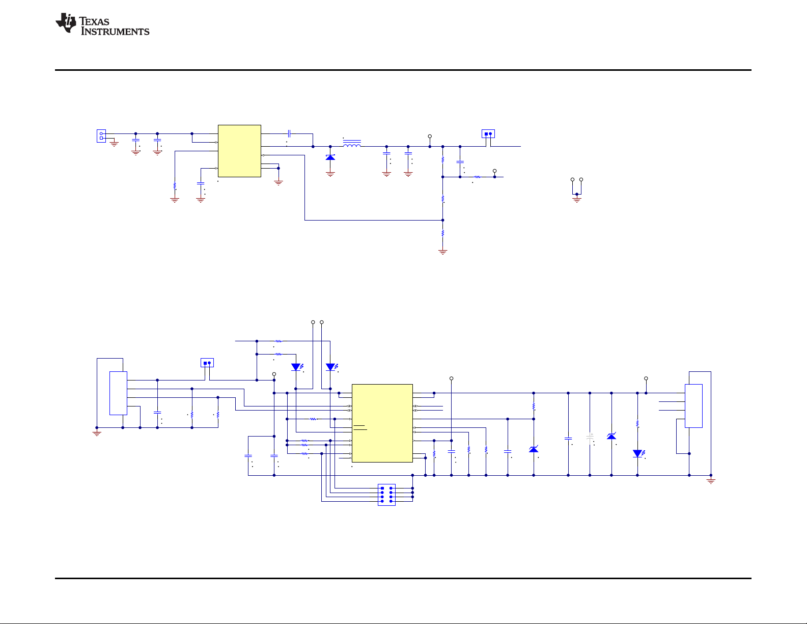
3 Schematic
Figure 1 illustrates the EVM schematic.
Schematic
SLVUB94–October 2017
Submit Documentation Feedback
TPS254900AQ1EVM-003 Evaluation Module
3
Figure 1. TPS254900AQ1EVM-003 Schematic
Copyright © 2017, Texas Instruments Incorporated
Page 4
General Configuration and Description
4 General Configuration and Description
4.1 Physical Access
Table 1 lists the TPS254900AQ1EVM-003 connector functionality, Table 2 describes the test point
availability and Table 3 describes the jumper functionality.
Table 1. Connector Functionality
Connector Label Description
J5 J5 Downstream facing USB 2.0 connector. Connect to the USB 2.0 slave for
data pass through from J4. USB output power is also provided to the slave.
J4 J4 Upstream facing USB 2.0 connector. Connect to the USB 2.0 host for data
pass through to J5. USB input power can also be provided by the host
when the J3 shunt is installed.
J1 J1 Automotive input voltage range connector. Connect to a 7 V–18 V, 1.5-A
voltage source according to the polarity marked on the EVM.
D2 (RED) D2 TPS254900A-Q1 FAULT output is triggered
D3 (BLUE) D3 TPS254900A-Q1 STATUS output is triggered
D6 (GREEN) D6 TPS254900A-Q1 output powered
Table 2. Test Points
Test Point Color Label Description
TP1 SM-L VDC TPS254900A-Q1 power switch input from DC-DC converter
TP2 SM-L CS Loop injection point
TP3 SM-L GND GND Test point
TP4 SM-L GND GND Test point
TP7 SM-L STATUS TPS254900A STATUS pin test point
TP8 SM-L FAULT TPS254900A FAULT pin test point
TP9 SM-L VIN TPS254900A VIN pin test point
TP10 SM-L OUT TPS254900A VBUS pin test point
TP11 SM-L IMON TPS254900A IMON pin test point
www.ti.com
Table 3. Jumpers
Jumper Label Description
J2 J2 Install to power TPS254900A-Q1 with a DC/DC
J3 J3 USB host furnished input voltage. Install to power TPS254900A-Q1 with a USB
J6 J6 TPS254900A-Q1 mode select jumper block. Install shunt at EN (1-2) to disable
4
TPS254900AQ1EVM-003 Evaluation Module
host.
TPS254900A-Q1. C1, C2, OVP_SEL positions select the charging mode for
TPS254900A-Q1. Refer to the data sheet for more information.
SLVUB94–October 2017
Copyright © 2017, Texas Instruments Incorporated
Submit Documentation Feedback
Page 5
+
PSIL003
J4
J1
J5
7" Twisted Pair, #20AWG
TP4
V
IN
Resistor Load
TP10
D6
D2
D3
+
±
±
Copyright © 2017, Texas Instruments Incorporated
www.ti.com
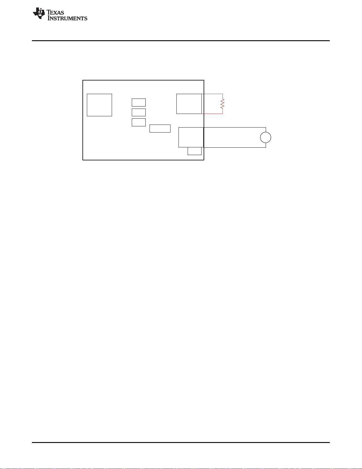
4.2 Test Setup
Figure 2 shows a typical test setup for TPS254900AQ1EVM-003. Connect J1 to the 14-V power supply.
The TPS254900A-Q1 output load can be applied either between TP10 and TP4 or via the USB 2.0 cable
plugged into J5.
General Configuration and Description
Figure 2. Typical TPS254900AQ1EVM-003 Test Setup
SLVUB94–October 2017
Submit Documentation Feedback
Copyright © 2017, Texas Instruments Incorporated
TPS254900AQ1EVM-003 Evaluation Module
5
Page 6

EVM Assembly Drawings and Layout Guidelines
5 EVM Assembly Drawings and Layout Guidelines
5.1 PCB Drawings
Figure 3 through Figure 8 show component placement and layout of the EVM.
www.ti.com
Figure 3. Top Side Placement Figure 4. Top Side Routing
Figure 5. Layer Two Routing Figure 6. Layer Three Routing
6
TPS254900AQ1EVM-003 Evaluation Module
Copyright © 2017, Texas Instruments Incorporated
SLVUB94–October 2017
Submit Documentation Feedback
Page 7

www.ti.com
EVM Assembly Drawings and Layout Guidelines
Figure 7. Bottom Side Routing Figure 8. Bottom Side Placement
SLVUB94–October 2017
Submit Documentation Feedback
TPS254900AQ1EVM-003 Evaluation Module
Copyright © 2017, Texas Instruments Incorporated
7
Page 8

EVM Assembly Drawings and Layout Guidelines
5.2 Layout Guidelines
Use the following layout guidelines:
• TPS254900A-Q1 placement: Place the TPS254900A-Q1 near the USB output connector and OUT pin
filter capacitors. Connect the exposed pad to the GND pin and the system ground plane using an array
of vias.
• IN pin bypass capacitance: Place the 0.1-μF bypass capacitor near the IN pin and make the
connection using a low inductance trace.
• DP-OUT, DM-OUT and DP-IN, DM-IN traces: Route these traces as controlled impedance differential
pairs per the USB-2.0 specification. Minimize the use of vias in the high-speed data lines. Figure 7
provides a good signal routing example for the high-speed data traces. In this example, the data pairs
are routed as edge-coupled microstrips with nominal differential impedance of 90 Ω. The reference
plane is tied to GND and is shown in Figure 6. Ensure that the reference plane is void of cuts or splits
above the differential pairs to prevent impedance discontinuities.
• ILIM_LO and ILIM_HI pin connections: Current-limit, set-point accuracy can be compromised by
stray current leakage from a higher voltage source to the ILIM_LO or ILIM_HI pins. Ensure that there is
adequate spacing between IN pin copper/trace and ILIM_LO pin trace to prevent contaminant buildup
during the PCB assembly process.
• The capacitor on BIAS helps improve IEC ESD performance, a 2.2-µF capacitor should be placed
close to BIAS and the whole “current” path from BIAS to GND across this capacitor should be as short
as possible. Do not use a via along the connection traces.
• A 10-µF output capacitor should be placed close to the OUT pin and TVS.
www.ti.com
5.3 EMI Containment
EMI containment methods are shown in the following list:
• Use compact loops for dv/dt and di/dt circuit paths (power loops and gate drives)
• Use minimal, yet thermally adequate, copper areas for heat sinking of components tied to switching
nodes (minimize exposed radiating surface).
• Use copper ground planes (possible stitching) and top-layer copper floods (surround circuitry with
ground floods)
• Use a 4-layer PCB, if economically feasible (for better grounding)
• Minimize the amount of copper area associated with input traces (to minimize radiated pickup)
• Maintain physical separation between input-related circuitry and power circuitry (use ferrite beads as
boundary line)
• Possible use of common-mode inductors
8
TPS254900AQ1EVM-003 Evaluation Module
Copyright © 2017, Texas Instruments Incorporated
SLVUB94–October 2017
Submit Documentation Feedback
Page 9

www.ti.com
6 Bill of Materials
Table 4 lists the EVM bill of materials.
Bill of Materials
Table 4. TPS254900AQ1EVM-003 Bill of Materials
Designator QTY Value Description Package Reference Part Number Manufacturer Alternate Part
!PCB 1 Printed Circuit Board PSIL003 Any - C1, C13, C16 3 0.1uF CAP, CERM, 0.1 µF, 16 V, +/- 10%, X7R, 0603 0603 GRM188R71C104KA01D Murata
C2 1 10uF CAP, CERM, 10 µF, 50 V, +/- 10%, X5R, 1210 1210 C3225X5R1H106K250AB TDK
C3 1 0.1uF CAP, CERM, 0.1 µF, 50 V, +/- 10%, X7R, 0603 0603 GRM188R71H104KA93D Murata
C4, C5 2 47uF CAP, CERM, 47 µF, 16 V, +/- 20%, X5R, 1210 1210 GRM32ER61C476ME15L Murata
C6, C7 2 0.022uF CAP, CERM, 0.022 µF, 16 V, +/- 10%, X7R, 0603 0603 C0603C223K4RACTU Kemet
C8, C15 2 10uF CAP, CERM, 10 µF, 16 V, +/- 10%, X7R, 1206 1206 GRM31CR71C106KAC7L Murata
C10 1 2.2uF CAP, CERM, 2.2 µF, 50 V, +/- 10%, X5R, 0603 0603 GRM188R61H225KE11D Murata
C11 1 10uF CAP, CERM, 10 µF, 35 V, +/- 10%, X7R, 1210 1210 GRM32ER7YA106KA12L Murata
D1 1 50V Diode, Schottky, 50 V, 3 A, SMA SMA B350A-13-F Diodes Inc.
D2 1 Red LED, Red, SMD SMD, 2-Leads, Body
D3 1 Blue LED, Blue, SMD BLUE 0603 LED LB Q39G-L2N2-35-1 OSRAM
D4, D5 2 18V Diode, TVS, Uni, 18 V, 400 W, SMA SMA SMAJ18A Littelfuse
D6 1 Green LED, Green, SMD 0.8x1.6mm HSMG-C190 Avago
J1 1 Conn Term Block, 2POS, 3.5mm, TH 11x8.5x7.3mm 1751248 Phoenix Contact
J2, J3 2 Header, 100mil, 2x1, Tin, TH Header, 2 PIN, 100mil,
J4 1 Connector, Plug, USB Type A, R/A, Top Mount SMT USB Type A right angle 48037-1000 Molex
J5 1 Connector, Receptacle, USB TYPE A, R/A, Top Mount
J6 1 Header, 100mil, 4x2, Tin, TH Header, 4x2, 100mil, Tin PEC04DAAN Sullins Connector
L1 1 10uH Inductor, Shielded Drum Core, Powdered Iron, 10 µH, 3 A,
R1 1 2.67k RES, 2.67 k, 1%, 0.1 W, 0603 0603 CRCW06032K67FKEA Vishay-Dale
R2 1 0 RES, 0, 5%, 0.1 W, 0603 0603 CRCW06030000Z0EA Vishay-Dale
R3 1 63.4k RES, 63.4 k, 1%, 0.1 W, 0603 0603 RC0603FR-0763K4L Yageo America
R4 1 29.4k RES, 29.4 k, 1%, 0.1 W, 0603 0603 CRCW060329K4FKEA Vishay-Dale
R5 1 5.62k RES, 5.62 k, 1%, 0.1 W, 0603 0603 CRCW06035K62FKEA Vishay-Dale
R6, R7 2 1.0k RES, 1.0 k, 5%, 0.1 W, 0603 0603 CRCW06031K00JNEA Vishay-Dale
R8, R9 2 15k RES, 15 k, 5%, 0.1 W, 0603 0603 CRCW060315K0JNEA Vishay-Dale
R10 1 5.1k RES, 5.1 k, 5%, 0.1 W, 0603 0603 CRCW06035K10JNEA Vishay-Dale
R11, R14, R15, R19 4 100k RES, 100 k, 1%, 0.1 W, 0603 0603 RC0603FR-07100KL Yageo America
R12 1 3.0k RES, 3.0 k, 5%, 0.1 W, 0603 0603 CRCW06033K00JNEA Vishay-Dale
R16 1 19.1k RES, 19.1 k, 1%, 0.1 W, 0603 0603 CRCW060319K1FKEA Vishay-Dale
(1)
Unless otherwise noted in the Alternate Part Number or Alternate Manufacturer columns, all parts may be substituted with equivalents.
SMT
0.075 ohm, SMD
1.3x0.8mm
Tin
USB TYPE A
CONNECTOR
RECEPTACLE 4POS
SMD
Inductor, 6.6x3x6.6mm 74437346100 Wurth Elektronik eiSos
LS L29K-G1J2-1-Z OSRAM
PEC02SAAN Sullins Connector
896-43-004-00-000000 Mill-Max
(1)
Number
Solutions
Solutions
Alternate
Manufacturer
SLVUB94–October 2017
Submit Documentation Feedback
Copyright © 2017, Texas Instruments Incorporated
TPS254900AQ1EVM-003 Evaluation Module
9
Page 10

Bill of Materials
www.ti.com
Table 4. TPS254900AQ1EVM-003 Bill of Materials
Designator QTY Value Description Package Reference Part Number Manufacturer Alternate Part
R17 1 80.6k RES, 80.6 k, 1%, 0.1 W, 0603 0603 CRCW060380K6FKEA Vishay-Dale
R18 1 2.55k RES, 2.55 k, 1%, 0.1 W, 0603 0603 CRCW06032K55FKEA Vishay-Dale
SH-J2, SH-J3 2 1x2 Shunt, 100mil, Gold plated, Black Shunt 969102-0000-DA 3M SNT-100-BK-G Samtec
TP1, TP2, TP3, TP4, TP7, TP8,
TP9, TP10, TP11
U1 1 SIMPLE SWITCHER 40 V 3.5 A, 2.2 MHz Step-Down
U2 1 Automotive USB Charging Port Controller and Power
C9 0 47uF CAP, AL, 47 µF, 35 V, +/- 20%, 0.44 ohm, SMD 6.3x5.8 UUD1V470MCL1GS Nichicon
FID1, FID2, FID3, FID4, FID5,
FID6
9 SMT Test Point, Miniature, SMT Testpoint_Keystone_Mini
Converter with 40 uA IQ, DDA0008E
Switch with Short to BAT protection, RVC0020A
0 Fiducial mark. There is nothing to buy or mount. Fiducial N/A N/A
ature
DDA0008E LMR14030SDDAR Texas Instruments LMR14030SDDA Texas Instruments
RVC0020A TPS254900IRVCRQ1 Texas Instruments TPS254900IRVCTQ1 Texas Instruments
(1)
(continued)
5015 Keystone
Number
Alternate
Manufacturer
10
TPS254900AQ1EVM-003 Evaluation Module
SLVUB94–October 2017
Submit Documentation Feedback
Copyright © 2017, Texas Instruments Incorporated
Page 11

STANDARD TERMS FOR EVALUATION MODULES
1. Delivery: TI delivers TI evaluation boards, kits, or modules, including any accompanying demonstration software, components, and/or
documentation which may be provided together or separately (collectively, an “EVM” or “EVMs”) to the User (“User”) in accordance
with the terms set forth herein. User's acceptance of the EVM is expressly subject to the following terms.
1.1 EVMs are intended solely for product or software developers for use in a research and development setting to facilitate feasibility
evaluation, experimentation, or scientific analysis of TI semiconductors products. EVMs have no direct function and are not
finished products. EVMs shall not be directly or indirectly assembled as a part or subassembly in any finished product. For
clarification, any software or software tools provided with the EVM (“Software”) shall not be subject to the terms and conditions
set forth herein but rather shall be subject to the applicable terms that accompany such Software
1.2 EVMs are not intended for consumer or household use. EVMs may not be sold, sublicensed, leased, rented, loaned, assigned,
or otherwise distributed for commercial purposes by Users, in whole or in part, or used in any finished product or production
system.
2 Limited Warranty and Related Remedies/Disclaimers:
2.1 These terms do not apply to Software. The warranty, if any, for Software is covered in the applicable Software License
Agreement.
2.2 TI warrants that the TI EVM will conform to TI's published specifications for ninety (90) days after the date TI delivers such EVM
to User. Notwithstanding the foregoing, TI shall not be liable for a nonconforming EVM if (a) the nonconformity was caused by
neglect, misuse or mistreatment by an entity other than TI, including improper installation or testing, or for any EVMs that have
been altered or modified in any way by an entity other than TI, (b) the nonconformity resulted from User's design, specifications
or instructions for such EVMs or improper system design, or (c) User has not paid on time. Testing and other quality control
techniques are used to the extent TI deems necessary. TI does not test all parameters of each EVM.
User's claims against TI under this Section 2 are void if User fails to notify TI of any apparent defects in the EVMs within ten (10)
business days after delivery, or of any hidden defects with ten (10) business days after the defect has been detected.
2.3 TI's sole liability shall be at its option to repair or replace EVMs that fail to conform to the warranty set forth above, or credit
User's account for such EVM. TI's liability under this warranty shall be limited to EVMs that are returned during the warranty
period to the address designated by TI and that are determined by TI not to conform to such warranty. If TI elects to repair or
replace such EVM, TI shall have a reasonable time to repair such EVM or provide replacements. Repaired EVMs shall be
warranted for the remainder of the original warranty period. Replaced EVMs shall be warranted for a new full ninety (90) day
warranty period.
3 Regulatory Notices:
3.1 United States
3.1.1 Notice applicable to EVMs not FCC-Approved:
FCC NOTICE: This kit is designed to allow product developers to evaluate electronic components, circuitry, or software
associated with the kit to determine whether to incorporate such items in a finished product and software developers to write
software applications for use with the end product. This kit is not a finished product and when assembled may not be resold or
otherwise marketed unless all required FCC equipment authorizations are first obtained. Operation is subject to the condition
that this product not cause harmful interference to licensed radio stations and that this product accept harmful interference.
Unless the assembled kit is designed to operate under part 15, part 18 or part 95 of this chapter, the operator of the kit must
operate under the authority of an FCC license holder or must secure an experimental authorization under part 5 of this chapter.
3.1.2 For EVMs annotated as FCC – FEDERAL COMMUNICATIONS COMMISSION Part 15 Compliant:
CAUTION
This device complies with part 15 of the FCC Rules. Operation is subject to the following two conditions: (1) This device may not
cause harmful interference, and (2) this device must accept any interference received, including interference that may cause
undesired operation.
Changes or modifications not expressly approved by the party responsible for compliance could void the user's authority to
operate the equipment.
FCC Interference Statement for Class A EVM devices
NOTE: This equipment has been tested and found to comply with the limits for a Class A digital device, pursuant to part 15 of
the FCC Rules. These limits are designed to provide reasonable protection against harmful interference when the equipment is
operated in a commercial environment. This equipment generates, uses, and can radiate radio frequency energy and, if not
installed and used in accordance with the instruction manual, may cause harmful interference to radio communications.
Operation of this equipment in a residential area is likely to cause harmful interference in which case the user will be required to
correct the interference at his own expense.
Page 12

FCC Interference Statement for Class B EVM devices
NOTE: This equipment has been tested and found to comply with the limits for a Class B digital device, pursuant to part 15 of
the FCC Rules. These limits are designed to provide reasonable protection against harmful interference in a residential
installation. This equipment generates, uses and can radiate radio frequency energy and, if not installed and used in accordance
with the instructions, may cause harmful interference to radio communications. However, there is no guarantee that interference
will not occur in a particular installation. If this equipment does cause harmful interference to radio or television reception, which
can be determined by turning the equipment off and on, the user is encouraged to try to correct the interference by one or more
of the following measures:
• Reorient or relocate the receiving antenna.
• Increase the separation between the equipment and receiver.
• Connect the equipment into an outlet on a circuit different from that to which the receiver is connected.
• Consult the dealer or an experienced radio/TV technician for help.
3.2 Canada
3.2.1 For EVMs issued with an Industry Canada Certificate of Conformance to RSS-210 or RSS-247
Concerning EVMs Including Radio Transmitters:
This device complies with Industry Canada license-exempt RSSs. Operation is subject to the following two conditions:
(1) this device may not cause interference, and (2) this device must accept any interference, including interference that may
cause undesired operation of the device.
Concernant les EVMs avec appareils radio:
Le présent appareil est conforme aux CNR d'Industrie Canada applicables aux appareils radio exempts de licence. L'exploitation
est autorisée aux deux conditions suivantes: (1) l'appareil ne doit pas produire de brouillage, et (2) l'utilisateur de l'appareil doit
accepter tout brouillage radioélectrique subi, même si le brouillage est susceptible d'en compromettre le fonctionnement.
Concerning EVMs Including Detachable Antennas:
Under Industry Canada regulations, this radio transmitter may only operate using an antenna of a type and maximum (or lesser)
gain approved for the transmitter by Industry Canada. To reduce potential radio interference to other users, the antenna type
and its gain should be so chosen that the equivalent isotropically radiated power (e.i.r.p.) is not more than that necessary for
successful communication. This radio transmitter has been approved by Industry Canada to operate with the antenna types
listed in the user guide with the maximum permissible gain and required antenna impedance for each antenna type indicated.
Antenna types not included in this list, having a gain greater than the maximum gain indicated for that type, are strictly prohibited
for use with this device.
Concernant les EVMs avec antennes détachables
Conformément à la réglementation d'Industrie Canada, le présent émetteur radio peut fonctionner avec une antenne d'un type et
d'un gain maximal (ou inférieur) approuvé pour l'émetteur par Industrie Canada. Dans le but de réduire les risques de brouillage
radioélectrique à l'intention des autres utilisateurs, il faut choisir le type d'antenne et son gain de sorte que la puissance isotrope
rayonnée équivalente (p.i.r.e.) ne dépasse pas l'intensité nécessaire à l'établissement d'une communication satisfaisante. Le
présent émetteur radio a été approuvé par Industrie Canada pour fonctionner avec les types d'antenne énumérés dans le
manuel d’usage et ayant un gain admissible maximal et l'impédance requise pour chaque type d'antenne. Les types d'antenne
non inclus dans cette liste, ou dont le gain est supérieur au gain maximal indiqué, sont strictement interdits pour l'exploitation de
l'émetteur
3.3 Japan
3.3.1 Notice for EVMs delivered in Japan: Please see http://www.tij.co.jp/lsds/ti_ja/general/eStore/notice_01.page 日本国内に
輸入される評価用キット、ボードについては、次のところをご覧ください。
http://www.tij.co.jp/lsds/ti_ja/general/eStore/notice_01.page
3.3.2 Notice for Users of EVMs Considered “Radio Frequency Products” in Japan: EVMs entering Japan may not be certified
by TI as conforming to Technical Regulations of Radio Law of Japan.
If User uses EVMs in Japan, not certified to Technical Regulations of Radio Law of Japan, User is required to follow the
instructions set forth by Radio Law of Japan, which includes, but is not limited to, the instructions below with respect to EVMs
(which for the avoidance of doubt are stated strictly for convenience and should be verified by User):
1. Use EVMs in a shielded room or any other test facility as defined in the notification #173 issued by Ministry of Internal
Affairs and Communications on March 28, 2006, based on Sub-section 1.1 of Article 6 of the Ministry’s Rule for
Enforcement of Radio Law of Japan,
2. Use EVMs only after User obtains the license of Test Radio Station as provided in Radio Law of Japan with respect to
EVMs, or
3. Use of EVMs only after User obtains the Technical Regulations Conformity Certification as provided in Radio Law of Japan
with respect to EVMs. Also, do not transfer EVMs, unless User gives the same notice above to the transferee. Please note
that if User does not follow the instructions above, User will be subject to penalties of Radio Law of Japan.
Page 13

【無線電波を送信する製品の開発キットをお使いになる際の注意事項】 開発キットの中には技術基準適合証明を受けて
いないものがあります。 技術適合証明を受けていないもののご使用に際しては、電波法遵守のため、以下のいずれかの
措置を取っていただく必要がありますのでご注意ください。
1. 電波法施行規則第6条第1項第1号に基づく平成18年3月28日総務省告示第173号で定められた電波暗室等の試験設備でご使用
いただく。
2. 実験局の免許を取得後ご使用いただく。
3. 技術基準適合証明を取得後ご使用いただく。
なお、本製品は、上記の「ご使用にあたっての注意」を譲渡先、移転先に通知しない限り、譲渡、移転できないものとします。
上記を遵守頂けない場合は、電波法の罰則が適用される可能性があることをご留意ください。 日本テキサス・イ
ンスツルメンツ株式会社
東京都新宿区西新宿6丁目24番1号
西新宿三井ビル
3.3.3 Notice for EVMs for Power Line Communication: Please see http://www.tij.co.jp/lsds/ti_ja/general/eStore/notice_02.page
電力線搬送波通信についての開発キットをお使いになる際の注意事項については、次のところをご覧ください。http:/
/www.tij.co.jp/lsds/ti_ja/general/eStore/notice_02.page
3.4 European Union
3.4.1 For EVMs subject to EU Directive 2014/30/EU (Electromagnetic Compatibility Directive):
This is a class A product intended for use in environments other than domestic environments that are connected to a
low-voltage power-supply network that supplies buildings used for domestic purposes. In a domestic environment this
product may cause radio interference in which case the user may be required to take adequate measures.
4 EVM Use Restrictions and Warnings:
4.1 EVMS ARE NOT FOR USE IN FUNCTIONAL SAFETY AND/OR SAFETY CRITICAL EVALUATIONS, INCLUDING BUT NOT
LIMITED TO EVALUATIONS OF LIFE SUPPORT APPLICATIONS.
4.2 User must read and apply the user guide and other available documentation provided by TI regarding the EVM prior to handling
or using the EVM, including without limitation any warning or restriction notices. The notices contain important safety information
related to, for example, temperatures and voltages.
4.3 Safety-Related Warnings and Restrictions:
4.3.1 User shall operate the EVM within TI’s recommended specifications and environmental considerations stated in the user
guide, other available documentation provided by TI, and any other applicable requirements and employ reasonable and
customary safeguards. Exceeding the specified performance ratings and specifications (including but not limited to input
and output voltage, current, power, and environmental ranges) for the EVM may cause personal injury or death, or
property damage. If there are questions concerning performance ratings and specifications, User should contact a TI
field representative prior to connecting interface electronics including input power and intended loads. Any loads applied
outside of the specified output range may also result in unintended and/or inaccurate operation and/or possible
permanent damage to the EVM and/or interface electronics. Please consult the EVM user guide prior to connecting any
load to the EVM output. If there is uncertainty as to the load specification, please contact a TI field representative.
During normal operation, even with the inputs and outputs kept within the specified allowable ranges, some circuit
components may have elevated case temperatures. These components include but are not limited to linear regulators,
switching transistors, pass transistors, current sense resistors, and heat sinks, which can be identified using the
information in the associated documentation. When working with the EVM, please be aware that the EVM may become
very warm.
4.3.2 EVMs are intended solely for use by technically qualified, professional electronics experts who are familiar with the
dangers and application risks associated with handling electrical mechanical components, systems, and subsystems.
User assumes all responsibility and liability for proper and safe handling and use of the EVM by User or its employees,
affiliates, contractors or designees. User assumes all responsibility and liability to ensure that any interfaces (electronic
and/or mechanical) between the EVM and any human body are designed with suitable isolation and means to safely
limit accessible leakage currents to minimize the risk of electrical shock hazard. User assumes all responsibility and
liability for any improper or unsafe handling or use of the EVM by User or its employees, affiliates, contractors or
designees.
4.4 User assumes all responsibility and liability to determine whether the EVM is subject to any applicable international, federal,
state, or local laws and regulations related to User’s handling and use of the EVM and, if applicable, User assumes all
responsibility and liability for compliance in all respects with such laws and regulations. User assumes all responsibility and
liability for proper disposal and recycling of the EVM consistent with all applicable international, federal, state, and local
requirements.
5. Accuracy of Information: To the extent TI provides information on the availability and function of EVMs, TI attempts to be as accurate
as possible. However, TI does not warrant the accuracy of EVM descriptions, EVM availability or other information on its websites as
accurate, complete, reliable, current, or error-free.
Page 14

6. Disclaimers:
6.1 EXCEPT AS SET FORTH ABOVE, EVMS AND ANY MATERIALS PROVIDED WITH THE EVM (INCLUDING, BUT NOT
LIMITED TO, REFERENCE DESIGNS AND THE DESIGN OF THE EVM ITSELF) ARE PROVIDED "AS IS" AND "WITH ALL
FAULTS." TI DISCLAIMS ALL OTHER WARRANTIES, EXPRESS OR IMPLIED, REGARDING SUCH ITEMS, INCLUDING BUT
NOT LIMITED TO ANY EPIDEMIC FAILURE WARRANTY OR IMPLIED WARRANTIES OF MERCHANTABILITY OR FITNESS
FOR A PARTICULAR PURPOSE OR NON-INFRINGEMENT OF ANY THIRD PARTY PATENTS, COPYRIGHTS, TRADE
SECRETS OR OTHER INTELLECTUAL PROPERTY RIGHTS.
6.2 EXCEPT FOR THE LIMITED RIGHT TO USE THE EVM SET FORTH HEREIN, NOTHING IN THESE TERMS SHALL BE
CONSTRUED AS GRANTING OR CONFERRING ANY RIGHTS BY LICENSE, PATENT, OR ANY OTHER INDUSTRIAL OR
INTELLECTUAL PROPERTY RIGHT OF TI, ITS SUPPLIERS/LICENSORS OR ANY OTHER THIRD PARTY, TO USE THE
EVM IN ANY FINISHED END-USER OR READY-TO-USE FINAL PRODUCT, OR FOR ANY INVENTION, DISCOVERY OR
IMPROVEMENT, REGARDLESS OF WHEN MADE, CONCEIVED OR ACQUIRED.
7. USER'S INDEMNITY OBLIGATIONS AND REPRESENTATIONS. USER WILL DEFEND, INDEMNIFY AND HOLD TI, ITS
LICENSORS AND THEIR REPRESENTATIVES HARMLESS FROM AND AGAINST ANY AND ALL CLAIMS, DAMAGES, LOSSES,
EXPENSES, COSTS AND LIABILITIES (COLLECTIVELY, "CLAIMS") ARISING OUT OF OR IN CONNECTION WITH ANY
HANDLING OR USE OF THE EVM THAT IS NOT IN ACCORDANCE WITH THESE TERMS. THIS OBLIGATION SHALL APPLY
WHETHER CLAIMS ARISE UNDER STATUTE, REGULATION, OR THE LAW OF TORT, CONTRACT OR ANY OTHER LEGAL
THEORY, AND EVEN IF THE EVM FAILS TO PERFORM AS DESCRIBED OR EXPECTED.
8. Limitations on Damages and Liability:
8.1 General Limitations. IN NO EVENT SHALL TI BE LIABLE FOR ANY SPECIAL, COLLATERAL, INDIRECT, PUNITIVE,
INCIDENTAL, CONSEQUENTIAL, OR EXEMPLARY DAMAGES IN CONNECTION WITH OR ARISING OUT OF THESE
TERMS OR THE USE OF THE EVMS , REGARDLESS OF WHETHER TI HAS BEEN ADVISED OF THE POSSIBILITY OF
SUCH DAMAGES. EXCLUDED DAMAGES INCLUDE, BUT ARE NOT LIMITED TO, COST OF REMOVAL OR
REINSTALLATION, ANCILLARY COSTS TO THE PROCUREMENT OF SUBSTITUTE GOODS OR SERVICES, RETESTING,
OUTSIDE COMPUTER TIME, LABOR COSTS, LOSS OF GOODWILL, LOSS OF PROFITS, LOSS OF SAVINGS, LOSS OF
USE, LOSS OF DATA, OR BUSINESS INTERRUPTION. NO CLAIM, SUIT OR ACTION SHALL BE BROUGHT AGAINST TI
MORE THAN TWELVE (12) MONTHS AFTER THE EVENT THAT GAVE RISE TO THE CAUSE OF ACTION HAS
OCCURRED.
8.2 Specific Limitations. IN NO EVENT SHALL TI'S AGGREGATE LIABILITY FROM ANY USE OF AN EVM PROVIDED
HEREUNDER, INCLUDING FROM ANY WARRANTY, INDEMITY OR OTHER OBLIGATION ARISING OUT OF OR IN
CONNECTION WITH THESE TERMS, , EXCEED THE TOTAL AMOUNT PAID TO TI BY USER FOR THE PARTICULAR
EVM(S) AT ISSUE DURING THE PRIOR TWELVE (12) MONTHS WITH RESPECT TO WHICH LOSSES OR DAMAGES ARE
CLAIMED. THE EXISTENCE OF MORE THAN ONE CLAIM SHALL NOT ENLARGE OR EXTEND THIS LIMIT.
9. Return Policy. Except as otherwise provided, TI does not offer any refunds, returns, or exchanges. Furthermore, no return of EVM(s)
will be accepted if the package has been opened and no return of the EVM(s) will be accepted if they are damaged or otherwise not in
a resalable condition. If User feels it has been incorrectly charged for the EVM(s) it ordered or that delivery violates the applicable
order, User should contact TI. All refunds will be made in full within thirty (30) working days from the return of the components(s),
excluding any postage or packaging costs.
10. Governing Law: These terms and conditions shall be governed by and interpreted in accordance with the laws of the State of Texas,
without reference to conflict-of-laws principles. User agrees that non-exclusive jurisdiction for any dispute arising out of or relating to
these terms and conditions lies within courts located in the State of Texas and consents to venue in Dallas County, Texas.
Notwithstanding the foregoing, any judgment may be enforced in any United States or foreign court, and TI may seek injunctive relief
in any United States or foreign court.
Mailing Address: Texas Instruments, Post Office Box 655303, Dallas, Texas 75265
Copyright © 2017, Texas Instruments Incorporated
Page 15

IMPORTANT NOTICE FOR TI DESIGN INFORMATION AND RESOURCES
Texas Instruments Incorporated (‘TI”) technical, application or other design advice, services or information, including, but not limited to,
reference designs and materials relating to evaluation modules, (collectively, “TI Resources”) are intended to assist designers who are
developing applications that incorporate TI products; by downloading, accessing or using any particular TI Resource in any way, you
(individually or, if you are acting on behalf of a company, your company) agree to use it solely for this purpose and subject to the terms of
this Notice.
TI’s provision of TI Resources does not expand or otherwise alter TI’s applicable published warranties or warranty disclaimers for TI
products, and no additional obligations or liabilities arise from TI providing such TI Resources. TI reserves the right to make corrections,
enhancements, improvements and other changes to its TI Resources.
You understand and agree that you remain responsible for using your independent analysis, evaluation and judgment in designing your
applications and that you have full and exclusive responsibility to assure the safety of your applications and compliance of your applications
(and of all TI products used in or for your applications) with all applicable regulations, laws and other applicable requirements. You
represent that, with respect to your applications, you have all the necessary expertise to create and implement safeguards that (1)
anticipate dangerous consequences of failures, (2) monitor failures and their consequences, and (3) lessen the likelihood of failures that
might cause harm and take appropriate actions. You agree that prior to using or distributing any applications that include TI products, you
will thoroughly test such applications and the functionality of such TI products as used in such applications. TI has not conducted any
testing other than that specifically described in the published documentation for a particular TI Resource.
You are authorized to use, copy and modify any individual TI Resource only in connection with the development of applications that include
the TI product(s) identified in such TI Resource. NO OTHER LICENSE, EXPRESS OR IMPLIED, BY ESTOPPEL OR OTHERWISE TO
ANY OTHER TI INTELLECTUAL PROPERTY RIGHT, AND NO LICENSE TO ANY TECHNOLOGY OR INTELLECTUAL PROPERTY
RIGHT OF TI OR ANY THIRD PARTY IS GRANTED HEREIN, including but not limited to any patent right, copyright, mask work right, or
other intellectual property right relating to any combination, machine, or process in which TI products or services are used. Information
regarding or referencing third-party products or services does not constitute a license to use such products or services, or a warranty or
endorsement thereof. Use of TI Resources may require a license from a third party under the patents or other intellectual property of the
third party, or a license from TI under the patents or other intellectual property of TI.
TI RESOURCES ARE PROVIDED “AS IS” AND WITH ALL FAULTS. TI DISCLAIMS ALL OTHER WARRANTIES OR
REPRESENTATIONS, EXPRESS OR IMPLIED, REGARDING TI RESOURCES OR USE THEREOF, INCLUDING BUT NOT LIMITED TO
ACCURACY OR COMPLETENESS, TITLE, ANY EPIDEMIC FAILURE WARRANTY AND ANY IMPLIED WARRANTIES OF
MERCHANTABILITY, FITNESS FOR A PARTICULAR PURPOSE, AND NON-INFRINGEMENT OF ANY THIRD PARTY INTELLECTUAL
PROPERTY RIGHTS.
TI SHALL NOT BE LIABLE FOR AND SHALL NOT DEFEND OR INDEMNIFY YOU AGAINST ANY CLAIM, INCLUDING BUT NOT
LIMITED TO ANY INFRINGEMENT CLAIM THAT RELATES TO OR IS BASED ON ANY COMBINATION OF PRODUCTS EVEN IF
DESCRIBED IN TI RESOURCES OR OTHERWISE. IN NO EVENT SHALL TI BE LIABLE FOR ANY ACTUAL, DIRECT, SPECIAL,
COLLATERAL, INDIRECT, PUNITIVE, INCIDENTAL, CONSEQUENTIAL OR EXEMPLARY DAMAGES IN CONNECTION WITH OR
ARISING OUT OF TI RESOURCES OR USE THEREOF, AND REGARDLESS OF WHETHER TI HAS BEEN ADVISED OF THE
POSSIBILITY OF SUCH DAMAGES.
You agree to fully indemnify TI and its representatives against any damages, costs, losses, and/or liabilities arising out of your noncompliance with the terms and provisions of this Notice.
This Notice applies to TI Resources. Additional terms apply to the use and purchase of certain types of materials, TI products and services.
These include; without limitation, TI’s standard terms for semiconductor products http://www.ti.com/sc/docs/stdterms.htm), evaluation
modules, and samples (http://www.ti.com/sc/docs/sampterms.htm).
Mailing Address: Texas Instruments, Post Office Box 655303, Dallas, Texas 75265
Copyright © 2017, Texas Instruments Incorporated
 Loading...