

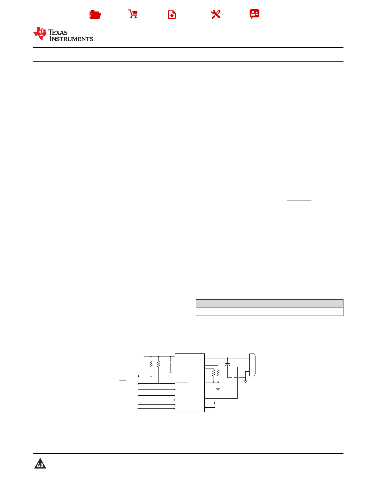
OUT
GND
FAULT
ILIM_LO
EN
R
ILIM_LO
R
STATUS
(10 kW)
Power Switch EN
4.5V – 5.5V
TPS2546
0.1 uF
C
USB
Fault Signal
DM_IN
DP_IN
VBUS
DD+
GND
USB
Connector
To Portable Device à
Power Bus
CTL1
CTL2
CTL3
ILIM_SEL
ILIM Select
DM_OUT
DP_OUT
To Host Controller à
Mode Select I/O
IN
STATUS
STATUS Signal
R
ILIM_HI
ILIM_HI
R
FAULT
(10 kW)
Product
Folder
Sample &
Buy
Technical
Documents
Tools &
Software
Support &
Community
TPS2546
SLVSBJ2B –FEBRUARY 2013–REVISED JANUARY 2016
TPS2546 USB Charging Port Controller and Power Switch With Load Detection
1 Features 2 Applications
1
• D+/D– CDP/DCP Modes per USB Battery
Charging Specification 1.2
• D+/D– Shorted Mode per Chinese
Telecommunication Industry Standard YD/T
1591-2009
• Supports Non-BC1.2 Charging Modes by The TPS2546 is a USB charging port controller and
Automatic Selection:
– D+/D– Divider Modes 2 V/2.7 V and 2.7 V/2 V
– D+/D– 1.2-V Mode
• Supports Sleep-Mode Charging and charging of popular mobile phones, tablets, and
Mouse/Keyboard Wakeup
• Automatic SDP/CDP Switching for Devices That
Do Not Connect to CDP Ports
• Load Detection for Power Supply Control in S4/S5
Charging and Port Power Management in All
Charge Modes
• Compatible With USB 2.0 and 3.0 Power Switch
Requirements
• Integrated 73-mΩ (Typical) High-Side MOSFET
• Adjustable Current-Limit up to 3 A (Typical)
• Operating Range: 4.5 V to 5.5 V
• Max Device Current:
– 2 µA When Device Disabled
– 270 µA When Device Enabled
• Drop-In and BOM Compatible With TPS2543
• Available in 16-Pin WQFN (3.00 mm × 3.00 mm)
Package
• 8-kV ESD Rating on DM/DP Pins
• UL Listed File No. E169910 and CB certified
• USB Ports (Host and Hubs)
• Notebook and Desktop PCs
• Universal Wall-Charging Adapters
3 Description
power switch with an integrated USB 2.0 high-speed
data line (D+/D–) switch. TPS2546 provides the
electrical signatures on D+/D– to support charging
schemes listed under Feature Description. TI tests
media devices with the TPS2546 to ensure
compatibility with both BC1.2 compliant, and nonBC1.2 compliant devices.
In addition to charging popular devices, the TPS2546
also supports two distinct power management
features, namely, power wake and port power
management (PPM) through the STATUS pin. Power
wake allows for power supply control in S4/S5
charging and PPM the ability to manage port power in
a multi-port application. Additionally, system wake up
(from S3) with a mouse/keyboard (both low speed
and full speed) is fully supported in the TPS2546.
The TPS2546 73-mΩ power-distribution switch is
intended for applications where heavy capacitive
loads and short-circuits are likely to be encountered.
Two programmable current thresholds provide
flexibility for setting current limits and load detect
thresholds.
Device Information
PART NUMBER PACKAGE BODY SIZE (NOM)
TPS2546 WQFN (16) 3.00 mm × 3.00 mm
(1) For all available packages, see the orderable addendum at
the end of the data sheet.
(1)
1
Simplified Schematic
An IMPORTANT NOTICE at the end of this data sheet addresses availability, warranty, changes, use in safety-critical applications,
intellectual property matters and other important disclaimers. PRODUCTION DATA.

TPS2546
SLVSBJ2B –FEBRUARY 2013–REVISED JANUARY 2016
www.ti.com
Table of Contents
1 Features.................................................................. 1
2 Applications ........................................................... 1
3 Description ............................................................. 1
4 Revision History..................................................... 2
5 Pin Configuration and Functions......................... 3
6 Specifications......................................................... 4
6.1 Absolute Maximum Ratings ...................................... 4
6.2 ESD Ratings.............................................................. 4
6.3 Recommended Operating Conditions....................... 4
6.4 Thermal Information.................................................. 5
6.5 Electrical Characteristics........................................... 5
6.6 Electrical Characteristics: High-Bandwidth Switch.... 6
6.7 Electrical Characteristics: Charging Controller ......... 7
6.8 Typical Characteristics.............................................. 9
7 Parameter Measurement Information ................ 12
8 Detailed Description............................................ 14
8.1 Overview ................................................................. 14
8.2 Functional Block Diagram ....................................... 15
8.3 Feature Description................................................. 15
8.4 Device Functional Modes........................................ 25
9 Application and Implementation ........................ 28
9.1 Application Information............................................ 28
9.2 Typical Application .................................................. 29
10 Power Supply Recommendations..................... 32
11 Layout................................................................... 32
11.1 Layout Guidelines ................................................. 32
11.2 Layout Example .................................................... 33
12 Device and Documentation Support ................. 34
12.1 Documentation Support ....................................... 34
12.2 Community Resources.......................................... 34
12.3 Trademarks........................................................... 34
12.4 Electrostatic Discharge Caution............................ 34
12.5 Glossary................................................................ 34
13 Mechanical, Packaging, and Orderable
Information........................................................... 34
4 Revision History
NOTE: Page numbers for previous revisions may differ from page numbers in the current version.
Changes from Revision A (Febuary 2013) to Revision B Page
• Added ESD Ratings table, Feature Description section, Device Functional Modes, Application and Implementation
section, Power Supply Recommendations section, Layout section, Device and Documentation Support section, and
Mechanical, Packaging, and Orderable Information section. ................................................................................................. 1
Changes from Original (February 2013) to Revision A Page
• Changed the device From: Preview To: Production............................................................................................................... 1
2 Submit Documentation Feedback Copyright © 2013–2016, Texas Instruments Incorporated
Product Folder Links: TPS2546
1
2
3
4
5 6 7 8
9
10
11
12
13141516
Thermal Pad
IN
DM_OUT
DP_OUT
EN
OUT
DM_IN
DP_IN
STATUS
ILIM_HI
ILIM_LO
GND
FAULT
www.ti.com
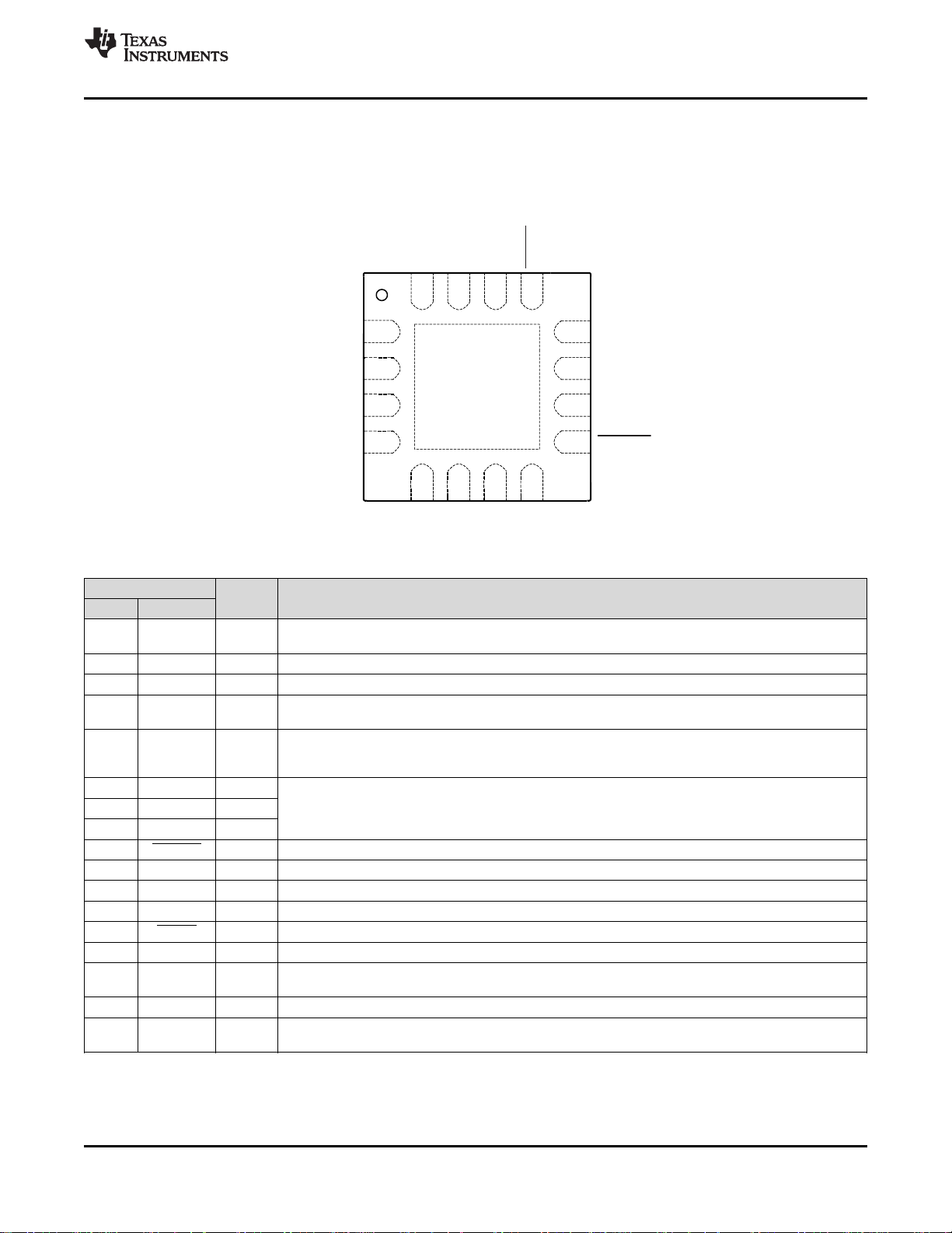
5 Pin Configuration and Functions
TPS2546
SLVSBJ2B –FEBRUARY 2013–REVISED JANUARY 2016
RTE Package
16-Pin WQFN
Top View
Pin Functions
PIN
NO. NAME
1 IN P
2 DM_OUT I/O D– data line to USB host controller.
3 DP_OUT I/O D+ data line to USB host controller.
4 ILIM_SEL I
5 EN I and power switches and holds OUT in discharge. Can be tied directly to IN or GND without pullup or
6 CTL1 I
7 CTL2 I
8 CTL3 I
9 STATUS O Active-low open-drain output, asserted in load detection conditions.
10 DP_IN I/O D+ data line to downstream connector.
11 DM_IN I/O D– data line to downstream connector.
12 OUT P Power-switch output.
13 FAULT O Active-low open-drain output, asserted during overtemperature or current limit conditions.
14 GND P Ground connection.
15 ILIM_LO I
16 ILIM_HI I External resistor connection used to set the high-current-limit threshold.
— —
(1) G = ground, I = input, O = output, P = power.
Thermal Internally connected to GND; used to heatsink the part to the circuit board traces. Connect to GND
Pad plane.
TYPE
(1)
Input voltage and supply voltage; connect 0.1 μF or greater ceramic capacitor from IN to GND as close
to the device as possible.
Logic-level input signal used to control the charging mode, current limit threshold, and load detection;
see Table 3. Can be tied directly to IN or GND without pullup or pulldown resistor.
Logic-level input for turning the power switch and the signal switches on/off; logic low turns off the signal
pulldown resistor.
Logic-level inputs used to control the charging mode and the signal switches; see Table 3. Can be tied
directly to IN or GND without pullup or pulldown resistor.
External resistor connection used to set the low current-limit threshold and the load detection current
threshold. A resistor to ILIM_LO is optional; see Current-Limit Settings in Detailed Description.
DESCRIPTION
Copyright © 2013–2016, Texas Instruments Incorporated Submit Documentation Feedback 3
Product Folder Links: TPS2546
TPS2546
SLVSBJ2B –FEBRUARY 2013–REVISED JANUARY 2016
www.ti.com
6 Specifications
6.1 Absolute Maximum Ratings
Over operating free-air temperature range (unless otherwise noted)
IN, EN, ILIM_LO, ILIM_HI, FAULT, STATUS,
Voltage V
Input clamp current DP_IN, DM_IN, DP_OUT, DM_OUT ±20 mA
Continuous current in SDP or CDP
mode
Continuous current in BC1.2 DCP mode DP_IN to DM_IN ±50 mA
Continuous output current OUT Internally limited
Continuous output sink current FAULT, STATUS 25 mA
Continuous output source current ILIM_LO, ILIM_HI Internally limited mA
Operating junction temperature, T
J
(1) Stresses beyond those listed under Absolute Maximum Ratings may cause permanent damage to the device. These are stress ratings
only, which do not imply functional operation of the device at these or any other conditions beyond those indicated under Recommended
Operating Conditions. Exposure to absolute-maximum-rated conditions for extended periods may affect device reliability.
ILIM_SEL, CTL1, CTL2, CTL3, OUT
IN to OUT –7 7
DP_IN, DM_IN, DP_OUT, DM_OUT –0.3 (IN + 0.3) or 5.7
DP_IN to DP_OUT or DM_IN to DM_OUT ±100 mA
(1)
MIN MAX UNIT
–0.3 7
–40 Internally limited °C
6.2 ESD Ratings
HBM ±2000
V
(ESD)
Electrostatic
discharge
Human-body model (HBM), per ANSI/ESDA/JEDEC JS-
(1)
001
Charged-device model (CDM), per JEDEC specification JESD22-C101
HBM wrt GND and each
other, DP_IN, DM_IN, ±8000 V
OUT
(2)
(1) JEDEC document JEP155 states that 500-V HBM allows safe manufacturing with a standard ESD control process.
(2) JEDEC document JEP157 states that 250-V CDM allows safe manufacturing with a standard ESD control process.
6.3 Recommended Operating Conditions
voltages are referenced to GND (unless otherwise noted)
MIN MAX UNIT
V
IN
V
IH
V
IL
I
OUT
R
ILIM_XX
T
J
Input voltage, IN 4.5 5.5 V
Input voltage, logic-level inputs, EN, CTL1, CTL2, CTL3, ILIM_SEL 0 5.5 V
Input voltage, data line inputs, DP_IN, DM_IN, DP_OUT, DM_OUT 0 V
High-level input voltage, EN, CTL1, CTL2, CTL3, ILIM_SEL 1.8 V
Low-level input voltage, EN, CTL1, CTL2, CTL3, ILIM_SEL 0.8 V
Continuous current, data line inputs, SDP or CDP mode, DP_IN to DP_OUT, DM_IN to
DM_OUT
Continuous current, data line inputs, BC1.2 DCP mode, DP_IN to DM_IN ±15 mA
Continuous output current, OUT 0 2.5 A
Continuous output sink current, FAULT, STATUS 0 10 mA
Current-limit set resistors 16.9 750 kΩ
Operating virtual junction temperature –40 125 °C
VALUE UNIT
±500
V
IN
±30 mA
4 Submit Documentation Feedback Copyright © 2013–2016, Texas Instruments Incorporated
Product Folder Links: TPS2546
TPS2546
www.ti.com
SLVSBJ2B –FEBRUARY 2013–REVISED JANUARY 2016
6.4 Thermal Information
TPS2546
THERMAL METRIC
(1)
RTE (WQFN) UNIT
16 PINS
R
θJA
R
θJC(top)
R
θJB
ψ
JT
ψ
JB
R
θJC(bot)
Junction-to-ambient thermal resistance 53.4 °C/W
Junction-to-case (top) thermal resistance 51.4 °C/W
Junction-to-board thermal resistance 17.2 °C/W
Junction-to-top characterization parameter 3.7 °C/W
Junction-to-board characterization parameter 20.7 °C/W
Junction-to-case (bottom) thermal resistance 3.9 °C/W
(1) For more information about traditional and new thermal metrics, see the Semiconductor and IC Package Thermal Metrics application
report, SPRA953.
6.5 Electrical Characteristics
Unless otherwise noted: –40 ≤ TJ≤ 125°C, 4.5 V ≤ VIN≤ 5.5 V, VEN= VIN, V
R
STATUS
= 10 kΩ, R
ILIM_HI
= 20 kΩ, R
= 80.6 kΩ. Positive currents are into pins. Typical values are at 25°C. All voltages
ILIM_LO
are with respect to GND.
PARAMETER TEST CONDITIONS MIN TYP MAX UNIT
POWER SWITCH
TJ= 25°C, I
R
DS(on)
ON resistance
(1)
–40°C ≤ TJ≤ 85°C, I
–40°C ≤ TJ≤ 125°C, I
t
t
t
t
I
r
f
on
off
REV
OUT voltage rise time 0.7 1 1.6
OUT voltage fall time 0.2 0.35 0.5
OUT voltage turnon time 2.7 4
OUT voltage turnoff time 1.7 3
Reverse leakage current 2 µA
VIN= 5 V, CL= 1 µF, RL= 100 Ω (see Figure 23 and
Figure 24)
VIN= 5 V, CL= 1 µF, RL= 100 Ω (see Figure 23 and
Figure 25)
V
= 5.5 V, VIN= VEN= 0 V, –40 ≤ TJ≤ 85°C,
OUT
Measure I
DISCHARGE
R
DCHG
t
DCHG_L
t
DCHG_S
OUT discharge resistance 400 500 630 Ω
Long OUT discharge hold time Time V
Short OUT discharge hold time Time V
OUT
OUT
EN, ILIMSEL, CTL1, CTL2, CTL3 INPUTS
Input pin rising logic threshold
voltage
Input pin falling logic threshold
voltage
Hysteresis
(2)
Input current Pin voltage = 0 V or 5.5 V –0.5 0.5 µA
ILIMSEL CURRENT LIMIT
V
ILIM_SEL
V
ILIM_SEL
V
ILIM_SEL
V
ILIM_SEL
V
ILIM_SEL
VIN= 5 V, R = 0.1Ω, lead length = 2 inches
(see Figure 27)
I
t
OS
IOS
OUT short-circuit current limit
Response time to OUT short-
(2)
circuit
(1)
(1) Pulse-testing techniques maintain junction temperature close to ambient temperature; Thermal effects must be taken into account
separately.
(2) These parameters are provided for reference only and do not constitute part of TI's published device specifications for purposes of TI's
product warranty.
= 2 A 73 84
OUT
= 2 A 73 105 mΩ
OUT
= 2 A 73 120
OUT
OUT
< 0.7 V (see Figure 26) 1.3 2 2.9 s
< 0.7 V (see Figure 26) 205 310 450 ms
= 0 V, R
= 0 V, R
= 0 V, R
= VIN, R
= VIN, R
= 210 kΩ 205 240 275
ILIM_LO
= 80.6 kΩ 575 625 680
ILIM_LO
= 22.1 kΩ 2120 2275 2430 mA
ILIM_LO
= 20 kΩ 2340 2510 2685
ILIM_HI
= 16.9 kΩ 2770 2970 3170
ILIM_HI
ILIM_SEL
= VIN, V
CTL1
= V
CTL2
= V
CTL3
1 1.35 1.7 V
0.85 1.15 1.45
= VIN. R
FAULT
ms
ms
200 mV
1.5 µs
=
Copyright © 2013–2016, Texas Instruments Incorporated Submit Documentation Feedback 5
Product Folder Links: TPS2546
TPS2546
SLVSBJ2B –FEBRUARY 2013–REVISED JANUARY 2016
Electrical Characteristics (continued)
www.ti.com
Unless otherwise noted: –40 ≤ TJ≤ 125°C, 4.5 V ≤ VIN≤ 5.5 V, VEN= VIN, V
R
STATUS
= 10 kΩ, R
ILIM_HI
= 20 kΩ, R
= 80.6 kΩ. Positive currents are into pins. Typical values are at 25°C. All voltages
ILIM_LO
are with respect to GND.
PARAMETER TEST CONDITIONS MIN TYP MAX UNIT
SUPPLY CURRENT
I
IN_OFF
I
IN_ON
UNDERVOLTAGE LOCKOUT
V
UVLO
FAULT
STATUS
THERMAL SHUTDOWN
Disabled IN supply current VEN= 0 V, V
V
= V
CTL1
V
= V
CTL1
Enabled IN supply current V
V
V
CTL1
CTL1
CTL1
= V
= V
= 0 V, V
= 0 V, –40 ≤ TJ≤ 85°C 0.1 2 µA
OUT
CTL2
CTL2
CTL2
CTL2
= VIN, V
= V
CTL3
= VIN, V
= VIN, V
CTL2
= V
= 0 V, V
CTL3
= VIN, V
= 0 V, V
CTL3
= VIN, V
CTL3
= V
CTL3
ILIM_SEL
IN
IN rising UVLO threshold voltage 3.9 4.1 4.3 V
Hysteresis
Output low voltage I
OFF-state leakage V
(2)
= 1 mA 100 mV
FAULT
= 5.5 V 1 µA
FAULT
Overcurrent FAULT rising and
falling deglitch
Output low voltage I
OFF-state leakage V
= 1 mA 100 mV
STATUS
= 5.5 V 1 µA
STATUS
Thermal shutdown threshold 155
Thermal shutdown threshold in
current-limit
Hysteresis
(2)
ILIM_SEL
ILIM_SEL
= VIN, V
= 0 V 165 220
CTL1
= V
CTL2
= V
CTL3
= 0 V 175 230
ILIM_SEL
ILIM_SEL
= V
= V
IN
IN
185 240 µA
195 250
215 270
100 mV
5 8.2 12 ms
135 °C
= VIN. R
20
FAULT
=
6.6 Electrical Characteristics: High-Bandwidth Switch
Unless otherwise noted: –40 ≤ TJ≤ 125°C, 4.5 V ≤ VIN≤ 5.5 V, VEN= VIN, V
R
STATUS
= 10 kΩ, R
ILIM_HI
= 20 kΩ, R
= 80.6 kΩ. Positive currents are into pins. Typical values are at 25°C. All voltages
ILIM_LO
are with respect to GND.
PARAMETER TEST CONDITIONS MIN TYP MAX UNIT
HIGH-BANDWIDTH ANALOG SWITCH
V
DP/DM switch ON resistance Ω
Switch resistance mismatch between
DP / DM channels
DP/DM switch OFF-state capacitance
DP/DM switch ON-state capacitance
O
X
IRR
TALK
OFF-state isolation
ON-state cross channel isolation
OFF-state leakage current 0.1 1.5 µA
BW Bandwidth (–3 dB)
t
pd
Propagation delay
(1)
(2)
(3)
(3)
(3)
(3)
DP/DM_OUT
V
DP/DM_OUT
V
DP/DM_OUT
V
DP/DM_OUT
VEN= 0 V, V
f = 1 MHz
V
DP/DM_IN
VEN= 0 V, f = 250 MHz 33 dB
f = 250 MHz 52 dB
VEN= 0 V, V
measure I
RL= 50 Ω 2.6 GHz
(1) The resistance in series with the parasitic capacitance to GND is typically 250 Ω.
(2) The resistance in series with the parasitic capacitance to GND is typically 150 Ω
(3) These parameters are provided for reference only and do not constitute part of TI's published device specifications for purposes of TI's
product warranty.
6 Submit Documentation Feedback Copyright © 2013–2016, Texas Instruments Incorporated
Product Folder Links: TPS2546
= 0 V, I
DP/DM_IN
= 2.4 V, I
= 0 V, I
= 2.4 V, I
DP/DM_IN
DP/DM_IN
DP/DM_IN
DP/DM_IN
= 0.3 V, Vac= 0.6 V
= 0.3 V, Vac= 0.6 V
DP/DM_IN
DP/DM_OUT
= 3.6 V, V
ILIM_SEL
= VIN, V
CTL1
= V
CTL2
= V
CTL3
= 30 mA 2 4
= –15 mA 3 6
= 30 mA 0.05 0.15
= –15 mA 0.05 0.15
,
pk–pk
, f = 1 MHz 5.4 6.2 pF
pk-pk
DP/DM_OUT
= 0 V,
0.25 ns
= VIN. R
FAULT
3 3.6 pF
=
Ω
www.ti.com
Electrical Characteristics: High-Bandwidth Switch (continued)
TPS2546
SLVSBJ2B –FEBRUARY 2013–REVISED JANUARY 2016
Unless otherwise noted: –40 ≤ TJ≤ 125°C, 4.5 V ≤ VIN≤ 5.5 V, VEN= VIN, V
R
STATUS
= 10 kΩ, R
ILIM_HI
= 20 kΩ, R
= 80.6 kΩ. Positive currents are into pins. Typical values are at 25°C. All voltages
ILIM_LO
ILIM_SEL
= VIN, V
CTL1
= V
CTL2
= V
CTL3
= VIN. R
FAULT
are with respect to GND.
PARAMETER TEST CONDITIONS MIN TYP MAX UNIT
t
SK
Skew between opposite transitions of the
same port (t
PHL
– t
PLH
)
0.1 0.2 ns
6.7 Electrical Characteristics: Charging Controller
Unless otherwise noted: –40 ≤ TJ≤ 125°C, 4.5 V ≤ VIN≤ 5.5 V, VEN= VIN, V
R
FAULT
= R
STATUS
= 10 kΩ, R
ILIM_HI
= 20 kΩ, R
= 80.6 kΩ. Positive currents are into pins. Typical values are at 25°C. All
ILIM_LO
voltages are with respect to GND.
PARAMETER TEST CONDITIONS MIN TYP MAX UNIT
SHORTED MODE (BC1.2 DCP)
DP_IN / DM_IN shorting resistance VCTL1 = VIN, VCTL2 = VCTL3 = 0 V 125 200 Ω
1.2 V MODE
DP_IN /DM_IN output voltage 1.19 1.25 1.31 V
DP_IN /DM_IN output impedance 60 75 94 kΩ
DIVIDER1 MODE
DP_IN divider1 output voltage 1.9 2 2.1 V
DM_IN divider1 output voltage 2.57 2.7 2.84 V
DP_IN output impedance 8 10.5 12.5 kΩ
DM_IN output impedance 8 10.5 12.5 kΩ
DIVIDER2 MODE
DP_IN divider2 output voltage 2.57 2.7 2.84 V
DM_IN divider2 output voltage 1.9 2 2.1 V
DP_IN output impedance 8 10.5 12.5 kΩ
DM_IN output impedance 8 10.5 12.5 kΩ
CHARGING DOWNSTREAM PORT
V
DM_SRC
V
DAT_REF
V
LGC_SRC
I
DP_SINK
DM_IN CDP output voltage –250 µA < I
DP_IN rising lower window threshold
for V
Hysteresis
DM_SRC
activation
(1)
DP_IN rising upper window threshold
for V
Hysteresis
DM_SRC
de-activation
(1)
DP_IN sink current V
LOAD DETECT – NON-POWER WAKE
I
LD
t
LD_SET
IOUT rising load detect current
threshold
Hysteresis
(1)
Load detect set time 140 200 275 ms
Load detect reset time 1.9 3 4.2 s
(1) These parameters are provided for reference only and do not constitute part of Texas Instrument's published device specifications for
purposes of Texas Instrument's product warranty.
VCTL1 = VIN, VCTL2 = VCTL3 = 0 V
VCTL1 = VIN, VCTL2 = VCTL3 = 0 V
IOUT = 1 A
VCTL1 = VCTL2 = VCTL3 =
VIN
VCTL1 = VCTL2 = VCTL3 = VIN
VCTL1 = VCTL2 = VCTL3 =
VIN
VCTL1 = VCTL2 = VCTL3 = VIN
ILIM_SEL
V
DP_IN
µA
DP_IN
= VIN, V
CTL1
= 0 V, V
CTL2
= V
CTL3
= VIN.
= 0.6 V,
< 0 0.5 0.6 0.7 V
DM_IN
0.25 0.4 V
50 mV
0.8 1 V
100 mV
= 0.6 V 40 70 100 µA
635 700 765 mA
50 mA
=
Copyright © 2013–2016, Texas Instruments Incorporated Submit Documentation Feedback 7
Product Folder Links: TPS2546

TPS2546
SLVSBJ2B –FEBRUARY 2013–REVISED JANUARY 2016
Electrical Characteristics: Charging Controller (continued)
www.ti.com
Unless otherwise noted: –40 ≤ TJ≤ 125°C, 4.5 V ≤ VIN≤ 5.5 V, VEN= VIN, V
R
FAULT
= R
STATUS
= 10 kΩ, R
ILIM_HI
= 20 kΩ, R
= 80.6 kΩ. Positive currents are into pins. Typical values are at 25°C. All
ILIM_LO
voltages are with respect to GND.
PARAMETER TEST CONDITIONS MIN TYP MAX UNIT
LOAD DETECT – POWER WAKE
I
OS_PW
Power wake short-circuit current limit 32 55 78 mA
I
falling power wake reset current
OUT
detection threshold
Reset current hysteresis
(1)
VCTL1 = VCTL2 = 0 V, VCTL3 = VIN
Power wake reset time 10.7 15 20.6 s
ILIM_SEL
= VIN, V
CTL1
= 0 V, V
CTL2
= V
CTL3
= VIN.
23 45 67 mA
5 mA
8 Submit Documentation Feedback Copyright © 2013–2016, Texas Instruments Incorporated
Product Folder Links: TPS2546

0
0.2
0.4
0.6
0.8
1
1.2
−40 −20 0 20 40 60 80 100
Junction Temperature (°C)
Disabled IN Supply Current (µA)
VIN = 5.5 V
G005
130
140
150
160
170
180
190
−40 −25 −10 5 20 35 50 65 80 95 110 125
Junction Temperature (°C)
Enabled IN Supply Current (µA)
VIN = 4.5 V
VIN = 5 V
VIN = 5.5 V
Device configured for SDP
V
ILIMSEL
= 0 V
G006
460
480
500
520
540
560
580
−40 −25 −10 5 20 35 50 65 80 95 110 125
Junction Temperature (°C)
OUT Discharge Resistance (Ω)
VIN = 4.5 V
VIN = 5 V
VIN = 5.5 V
G003
0
500
1000
1500
2000
2500
3000
3500
−40 −25 −10 5 20 35 50 65 80 95 110 125
Junction Temperature (°C)
OUT Short Circuit Current Limit (mA)
R
ILIM_LO
= 210 kΩ
R
ILIM_LO
= 80.6 kΩ
R
ILIM_HI
= 20 kΩ
R
ILIM_HI
= 16.9 kΩ
G004
50
60
70
80
90
100
−40 −25 −10 5 20 35 50 65 80 95 110 125
Junction Temperature (°C)
On Resistance (mΩ)
G001
0
0.05
0.1
0.15
0.2
0.25
0.3
−40 −25 −10 5 20 35 50 65 80 95 110 125
Junction Temperature (°C)
Reverse Leakage Current (µA)
G002
www.ti.com
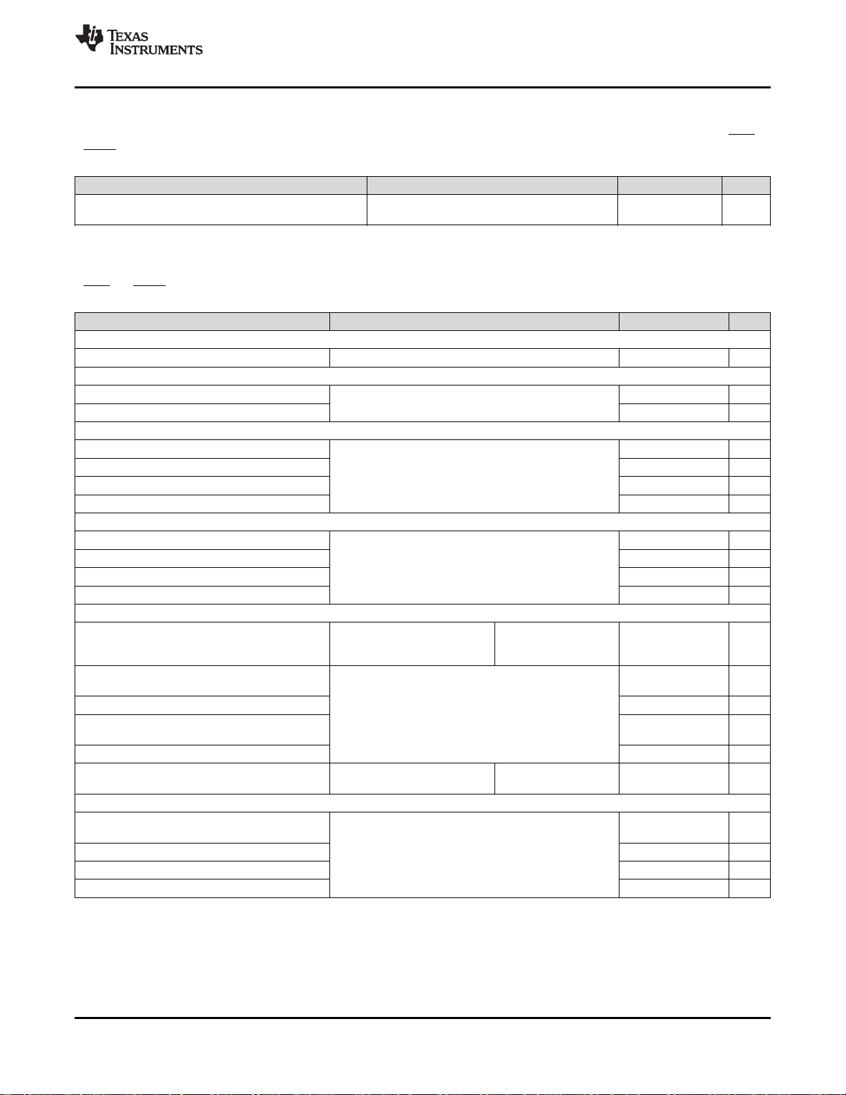
6.8 Typical Characteristics
Figure 1. Power Switch ON Resistance vs Temperature Figure 2. Reverse Leakage Current vs Temperature
TPS2546
SLVSBJ2B –FEBRUARY 2013–REVISED JANUARY 2016
Figure 3. OUT Discharge Resistance vs Temperature Figure 4. OUT Short-Circuit Current Limit vs Temperature
Figure 5. Disabled in Supply Current vs Temperature Figure 6. Enabled in Supply Current - SDP vs Temperature
Copyright © 2013–2016, Texas Instruments Incorporated Submit Documentation Feedback 9
Product Folder Links: TPS2546
0
60
O
IRR
- Off State Isolation - dB
10
40
20
50
0.01 1
Frequency - GHz
0.1 10
30
0
60
X
TALK
- ON State Cross-Channel Isolation - dB
10
40
20
50
0.01 1
Frequency - GHz
0.1 10
30
80
70
-20
0
Transmission Gain - dB
-20
-10
-15
-5
0.01 1
Frequency - GHz
0.1 10
0
100
200
300
400
500
600
700
0 1 2 3 4 5 6 7 8 9 10
Sinking Current (mA)
Output Low Voltage (mV)
TJ = −40°C
TJ = 25°C
TJ = 125°C
VIN = 4.5 V
G009
160
170
180
190
200
210
220
−40 −25 −10 5 20 35 50 65 80 95 110 125
Junction Temperature (°C)
Enabled IN Supply Current (µA)
VIN = 4.5 V
VIN = 5 V
VIN = 5.5 V
Device configured for CDP
G007
180
190
200
210
220
230
240
−40 −25 −10 5 20 35 50 65 80 95 110 125
Junction Temperature (°C)
Enabled IN Supply Current (µA)
VIN = 4.5 V
VIN = 5 V
VIN = 5.5 V
Device configured for DCP AUTO
G008
TPS2546
SLVSBJ2B –FEBRUARY 2013–REVISED JANUARY 2016
Typical Characteristics (continued)
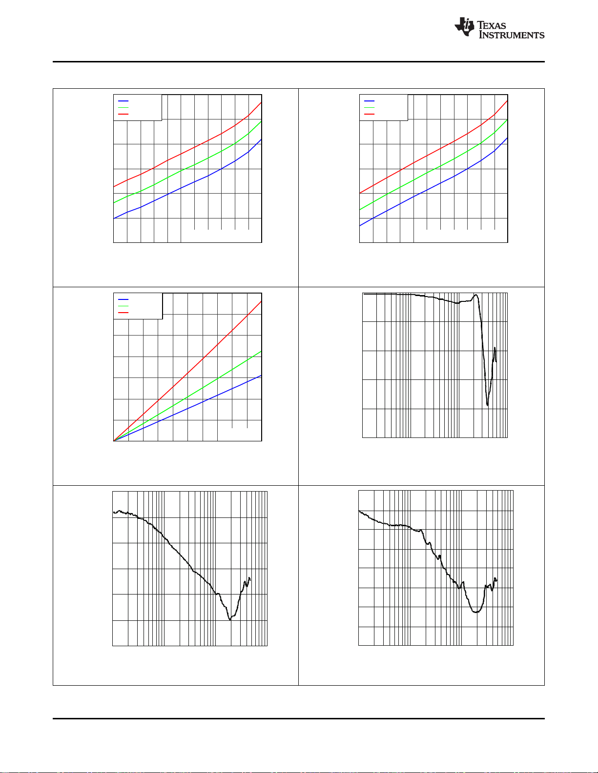
Figure 7. Enabled in Supply Current - CDP vs Temperature Figure 8. Enabled in Supply Current - DCP Auto
vs Temperature
www.ti.com
Figure 9. Status and Fault Output Low Voltage
Figure 11. OFF-State Data Switch Isolation vs Frequency
10 Submit Documentation Feedback Copyright © 2013–2016, Texas Instruments Incorporated
vs Sinking Current
Figure 10. Data Transmission Characteristics vs Frequency
Figure 12. ON-State Cross-Channel Isolation vs Frequency
Product Folder Links: TPS2546
I
IN
V
5 V/div
EN
V
2 V/div
OUT
t - Time - 1 ms/div
R
LOAD
= 5
C = 150 FΩµ
LOAD
G021
52
53
54
55
56
57
58
59
−40 −25 −10 5 20 35 50 65 80 95 110 125
Junction Temperature (°C)
Power Wake Current Limit (mA)
G017
600
620
640
660
680
700
720
740
−40 −25 −10 5 20 35 50 65 80 95 110 125
Junction Temperature (°C)
Current (mA)
IOS - OUT Short Circuit Current Limit
ILD - I
OUT
Rising Load Detect Threshold
R
ILIM_LO
= 80.6 kΩ
G015
200
205
210
215
220
225
230
−40 −25 −10 5 20 35 50 65 80 95 110 125
Junction Temperature (°C)
Load Detect Set Time (ms)
G016
G013
0.5
0.4
0.3
0.2
0.1
0
–0.1
–0.2
–0.3
–0.4
–0.5
0 0.2 0.4 0.6 0.8 1 1.2 1.4 1.6 1.8 2
Time (ns)
Differential Signal (V)
G014
0.5
0.4
0.3
0.2
0.1
0
–0.1
–0.2
–0.3
–0.4
–0.5
0 0.2 0.4 0.6 0.8 1 1.2 1.4 1.6 1.8 2
Time (ns)
Differential Signal (V)
www.ti.com
SLVSBJ2B –FEBRUARY 2013–REVISED JANUARY 2016
Typical Characteristics (continued)
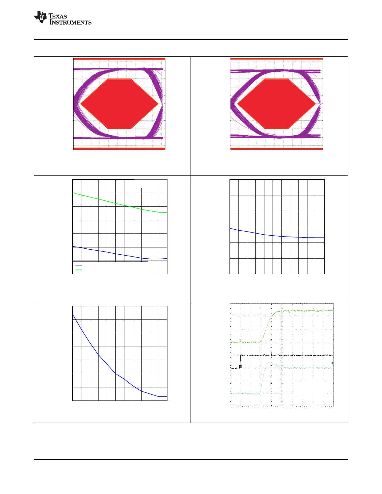
Figure 13. Eye Diagram Using USB Compliance Test Pattern Figure 14. Eye Diagram Using USB Compliance Test Pattern
(With No Switch) (With Data Switch)
TPS2546
Figure 15. IOUT Rising Load Detect Threshold and Out Figure 16. Load Detect Set Time vs Temperature
Short-Circuit Current Limit vs Temperature
Copyright © 2013–2016, Texas Instruments Incorporated Submit Documentation Feedback 11
Figure 17. Power Wake Current Limit vs Temperature
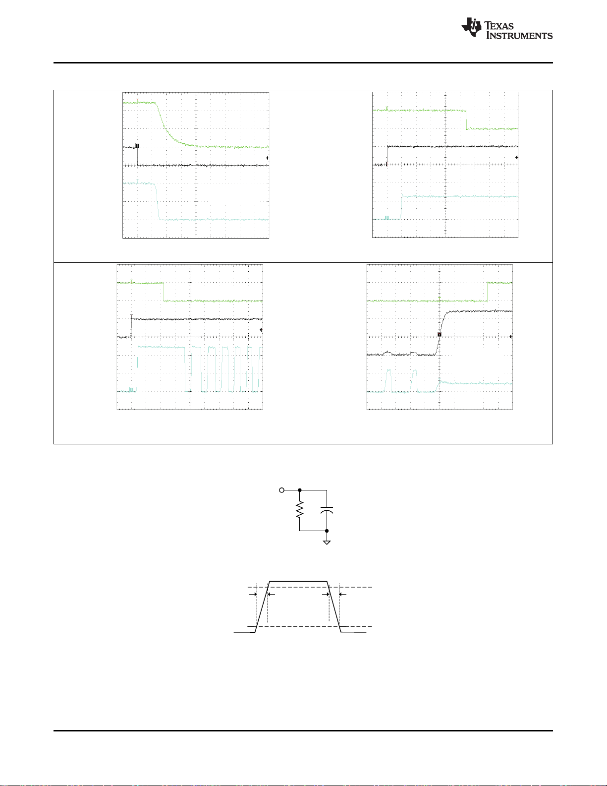
Figure 18. Turnon Response
Product Folder Links: TPS2546
10%
90%
V
OUT
t
r
t
f
R
L
C
L
I
1 A/div
IN
V
5 V/div
EN
V
5 V/div
/FAULT
t - Time - 5 ms/div
R
ILM_HI
= 20 kΩ
G024
I
2 A/div
IN
V
2 V/div
OUT
V
5 V/div
/FAULT
t - Time - 2 ms/div
R
ILIM_HI
LOAD
LOAD
= 20 k
R = 5
C = 150 F
Ω
Ω
µ
G025
I
IN
V
5 V/div
EN
V
2 V/div
OUT
t - Time - 1 ms/div
R
LOAD
= 5
C = 150 FΩµ
LOAD
G022
I
IN
V
5 V/div
EN
V
5 V/div
/FAULT
t - Time - 2 ms/div
R
ILM_LO
= 80.6 kΩ
G023
TPS2546
SLVSBJ2B –FEBRUARY 2013–REVISED JANUARY 2016
Typical Characteristics (continued)
www.ti.com
Figure 19. Turnoff Response
Figure 21. Device Enabled Into Short-Circuit - Thermal Figure 22. Short-Circuit to Full Load Recovery
Cycling
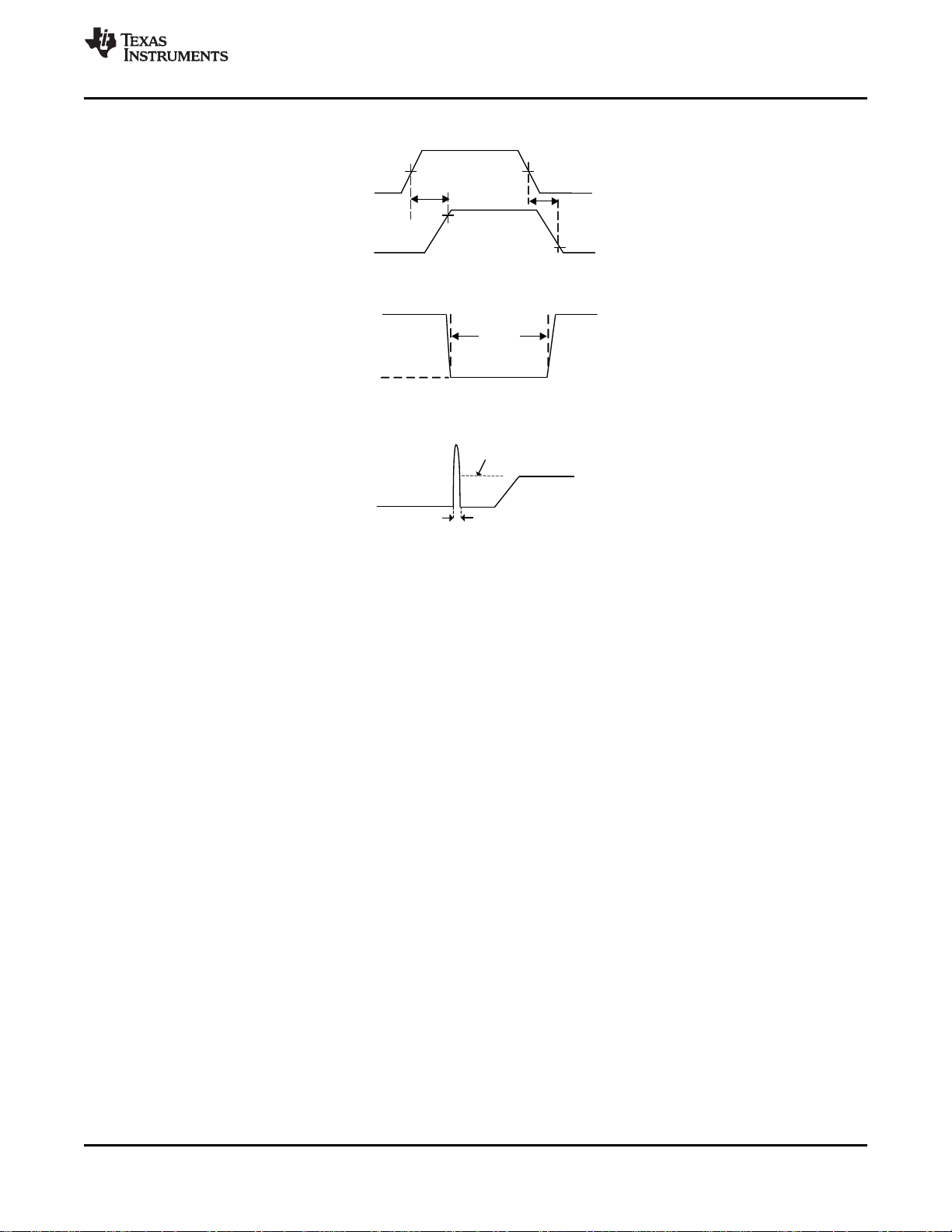
7 Parameter Measurement Information
Figure 20. Device Enabled Into Short-Circuit
Figure 23. Out Rise/Fall Test Load
Figure 24. Power-ON and OFF Timing
12 Submit Documentation Feedback Copyright © 2013–2016, Texas Instruments Incorporated
Product Folder Links: TPS2546
t
IOS
I
OUT
I
OS
5 V
V
OUT
0 V
t
DCHG
V
EN
V
OUT
t
on
50 %
50 %
t
off
90 %
10 %
www.ti.com
TPS2546
SLVSBJ2B –FEBRUARY 2013–REVISED JANUARY 2016
Parameter Measurement Information (continued)
Figure 25. Enable Timing, Active High Enable
Figure 26. Out Discharge During Mode Change
Figure 27. Output Short-Circuit Parameters
Copyright © 2013–2016, Texas Instruments Incorporated Submit Documentation Feedback 13
Product Folder Links: TPS2546

TPS2546
SLVSBJ2B –FEBRUARY 2013–REVISED JANUARY 2016
www.ti.com
8 Detailed Description
8.1 Overview
The following overview references various industry standards. TI recommends consulting the most up-to-date
standard to ensure the most recent and accurate information. Rechargeable portable equipment requires an
external power source to charge its batteries. USB ports are a convenient location for charging, because of an
available 5-V power source. Universally accepted standards are required to make sure host and client-side
devices operate together in a system to ensure power management requirements are met. Traditionally, host
ports following the USB 2.0 specification must provide at least 500 mA to downstream client-side devices.
Because multiple USB devices can attach to a single USB port through a bus-powered hub, it is the responsibility
of the client-side device to negotiate its power allotment from the host, ensuring the total current draw does not
exceed 500 mA. In general, each USB device is granted 100 mA, and may request more current in 100-mA unit
steps up to 500 mA. The host may grant or deny based on the available current. A USB 3.0 host port not only
provides higher data rate than USB 2.0 port, but also raises the unit load from 100 mA to 150 mA. It is also
required to provide a minimum current of 900 mA to downstream client-side devices.
Additionally, the success of USB makes the mini-USB connector a popular choice for wall adapter cables. This
allows a portable device to charge from both a wall adapter, and USB port with only one connector. As USB
charging has gained popularity, the 500-mA minimum defined by USB 2.0 or 900 mA for USB 3.0 has become
insufficient for many handset and personal media players, which need a higher charging rate. Wall adapters can
provide much more current than 500 mA/900 mA. Several new standards have been introduced, defining
protocol handshaking methods that allow host and client devices to acknowledge and draw additional current
beyond the 500 mA/900 mA minimum defined by USB 2.0 and 3.0, while still using a single micro-USB input
connector.
The TPS2546 supports four of the most common USB charging schemes found in popular handheld media and
cellular devices:
• USB Battery Charging Specification BC1.2
• Chinese Telecommunications Industry Standard YD/T 1591-2009
• Divider Mode
• 1.2-V Mode
YD/T 1591-2009 is a subset of BC1.2 specifications supported by vast majority of devices that implement USB
changing. Divider and 1.2-V charging schemes are supported in devices from specific, yet popular device
makers.
BC1.2 lists three different port types:
• Standard Downstream Port (SDP)
• Charging Downstream Port (CDP)
• Dedicated Charging Port (DCP)
BC1.2 defines a charging port as a downstream facing USB port that provides power for charging portable
equipment. Under this definition, CDP and DCP are defined as charging ports.
14 Submit Documentation Feedback Copyright © 2013–2016, Texas Instruments Incorporated
Product Folder Links: TPS2546

Disable + UVLO+Discharge
Driver
CS
Current
Limit
Charge
Pump
UVLO
Thermal
Sense
8-ms Deglitch
OTSD
Current
Sense
IN
EN
ILIM_HI
CTL1
DP_IN
DM_IN
OUT
GND
FAULT
8-ms Deglitch
(falling edge)
Current Limit
select
ILIM_LO
STATUS
DP_OUT
CTL2
CTL3
Logic
control
CDP
Detection
DCP
Detection
Auto-Detection
Divider
Mode
ILIM_SEL
Discharge
discharge
LD cur set
LD cur set
Discharge
OC
OC
www.ti.com
8.2 Functional Block Diagram
TPS2546
SLVSBJ2B –FEBRUARY 2013–REVISED JANUARY 2016
8.3 Feature Description
8.3.1 Standard Downstream Port (SDP) USB 2.0/USB 3.0
An SDP is a traditional USB port that follows USB 2.0 and 3.0 protocol, and supplies a minimum of 500 mA for
USB 2.0 and 900 mA for USB 3.0 per port. USB 2.0 and 3.0 communications is supported, and the host
controller must be active to allow charging. TPS2546 supports SDP mode in system power state S0, when
system is completely powered ON, and fully operational. For more details on control pin (CTL1-CTL3) settings to
program this state, see Table 3.
8.3.2 Charging Downstream Port (CDP)
A CDP is a USB port that follows USB BC1.2 and supplies a minimum of 1.5 A per port. It provides power and
meets USB 2.0 requirements for device enumeration. USB 2.0 communications is supported, and the host
controller must be active to allow charging. What separates a CDP from an SDP is the host-charge handshaking
logic that identifies this port as a CDP. A CDP is identifiable by a compliant BC1.2 client device, and allows for
additional current draw by the client device.
Copyright © 2013–2016, Texas Instruments Incorporated Submit Documentation Feedback 15
Product Folder Links: TPS2546

Auto
Detect
CDP
Detect
2.0V
2.7V
USB
Connector
D-
D+
VBUS
GND
D- Out
D+ Out
USB Host/Hub
1.2V
<200Ÿ
TPS2546
TPS2546
SLVSBJ2B –FEBRUARY 2013–REVISED JANUARY 2016
www.ti.com
Feature Description (continued)
The CDP process is done in two steps. During step one, the portable equipment outputs a nominal 0.6-V output
on the D+ line, and reads the voltage input on the D– line. The portable device detects it is connected to an SDP
if the voltage is less than the nominal data detect voltage of 0.3 V. The portable device detects that it is
connected to a Charging Port if the D– voltage is greater than the nominal data detect voltage of 0.3 V, and
optionally less than 0.8 V.
The second step is necessary for portable equipment to determine if it is connected to CDP or DCP. The
portable device outputs a nominal 0.6 V output on its D– line, and reads the voltage input on its D+ line. The
portable device detects it is connected to a CDP if the data line being read remains less than the nominal data
detect voltage of 0.3 V. The portable device detects it is connected to a DCP if the data line being read is greater
than the nominal data detect voltage of 0.3 V.
TPS2546 supports CDP mode in system power state S0 when system is completely powered ON, and fully
operational. For more details on control pin (CTL1-CTL3) settings to program this state, see Table 3.
8.3.3 Dedicated Charging Port (DCP)
A DCP only provides power but does not support data connection to an upstream port. As shown in following
sections, a DCP is identified by the electrical characteristics of the data lines. The TPS2546 emulates DCP in
two charging states, namely DCP Forced and DCP Auto as shown in Figure 32. In DCP Forced state the device
supports one of the two DCP charging schemes, namely Divider1 or Shorted. In the DCP Auto state, the device
charge detection state machine is activated to selectively implement charging schemes involved with the
Shorted, Divider1, Divider2, and 1.2-V modes. Shorted DCP mode complies with BC1.2 and Chinese
Telecommunications Industry Standard YD/T 1591-2009, while the Divider and 1.2-V modes are employed to
charge devices that do not comply with BC1.2 DCP standard.
8.3.3.1 DCP BC1.2 and YD/T 1591-2009
Both standards define that the D+ and D– data lines must be shorted together with a maximum series impedance
of 200 Ω. This is shown in Figure 28.
Figure 28. DCP Supporting BC1.2/YD/T 1591-2009
8.3.3.2 DCP Divider Charging Scheme
There are two Divider charging scheme supported by the device, Divider1 and Divider2 as shown in Figure 29
and Figure 30. In Divider1 charging scheme the device applies 2 V and 2.7 V to D+ and D– data line
respectively. This is reversed in Divider2 mode.
16 Submit Documentation Feedback Copyright © 2013–2016, Texas Instruments Incorporated
Product Folder Links: TPS2546

Auto
Detect
CDP
Detect
2.0V
2.7V
USB
Connector
D-
D+
VBUS
GND
D- Out
D+ Out
USB Host/Hub
1.2V
<200Ÿ
TPS2546
Auto
Detect
CDP
Detect
2.0V
2.7V
USB
Connector
D-
D+
VBUS
GND
D- Out
D+ Out
USB Host/Hub
1.2V
<200Ÿ
TPS2546
Auto
Detect
CDP
Detect
2.7V
2.0V
USB
Connector
D-
D+
VBUS
GND
D- Out
D+ Out
USB Host/Hub
1.2V
<200Ÿ
TPS2546
www.ti.com
Feature Description (continued)
Figure 29. DCP Divider1 Charging Scheme
TPS2546
SLVSBJ2B –FEBRUARY 2013–REVISED JANUARY 2016
Figure 30. Divider2 Charging Scheme
8.3.3.3 DCP 1.2-V Charging Scheme
1.2-V charging scheme is used by some handheld devices to enable fast charging at 2 A. TPS2546 supports this
scheme in the DCP-Auto mode before the device enters BC1.2 shorted mode. To simulate this charging scheme
D+/D– lines are shorted and pulled-up to 1.2 V for fixed duration then device moves to DCP shorted mode as
defined in BC1.2 specification. This is shown in Figure 31
Copyright © 2013–2016, Texas Instruments Incorporated Submit Documentation Feedback 17
Figure 31. DCP 1.2-V Charging Scheme
Product Folder Links: TPS2546

TPS2546
SLVSBJ2B –FEBRUARY 2013–REVISED JANUARY 2016
www.ti.com
Feature Description (continued)
8.3.4 Wake on USB Feature (Mouse/Keyboard Wake Feature)
8.3.4.1 USB 2.0 Background Information
The TPS2546 data lines interface with USB 2.0 devices. USB 2.0 defines three types of devices according to
data rate. These devices and their characteristics relevant to TPS2546 Wake on USB operation are shown
below.
Low-speed USB devices:
• 1.5 Mbps
• Wired mice and keyboards are examples
• No devices that need battery charging
• All signaling performed at 2 V and 0.8 V hi/lo logic levels
• D– high to signal connect and when placed into suspend
• D– high when not transmitting data packets
Full-speed USB devices:
• 12 Mbps
• Wireless mice and keyboards are examples
• Legacy phones and music players are examples
• Some legacy devices that need battery charging
• All signaling performed at 2 V and 0.8 V hi/lo logic levels
• D+ high to signal connect and when placed into suspend
• D+ high when not transmitting data packets
High-speed USB devices:
• 480 Mbps
• Tablets, phones and music players are examples
• Many devices that need battery charging
• Connect and suspend signaling performed at 2 V and 0.8 V hi/lo logic levels
• Data packet signaling performed a logic levels below 0.8 V
• D+ high to signal connect and when placed into suspend (same as a full-speed device)
• D+ and D– low when not transmitting data packets
8.3.4.2 Wake On USB
Wake on USB is the ability of a wake configured USB device to wake a computer system from its S3 sleep state
back to its S0 working state. Wake on USB requires the data lines to be connected to the system USB host
before the system is placed into its S3 sleep state, and remain continuously connected until they are used to
wake the system.
The TPS2546 supports low-speed and high-speed HID (human interface device like mouse/key board) wake
function. There are two scenarios under which wake on mouse are supported by the TPS2546. The specific CTL
pin changes that the TPS2546 overrides are shown below. The information is presented as CTL1, CTL2, CTL3.
The ILIM_SEL pin plays no role
1. 111 (CDP/SDP2) to 011 (DCP-Auto)
2. 010 (SDP1) to 011 (DCP-Auto)
NOTE
The 110 (SDP1) to 011 (DCP-Auto) transition is not supported. This is done for practical
reasons, because the transition involves changes to two CTL pins. Depending on which
CTL pin changes first, the device sees either a temporary 111 or 010 command. The 010
command is safe but the 111 command causes an OUT discharge as the TPS2546
instead proceeds to the 111 state.
18 Submit Documentation Feedback Copyright © 2013–2016, Texas Instruments Incorporated
Product Folder Links: TPS2546

TPS2546
www.ti.com
SLVSBJ2B –FEBRUARY 2013–REVISED JANUARY 2016
Feature Description (continued)
8.3.4.3 USB Slow-Speed and Full-Speed Device Recognition
TPS2546 is capable of detecting LS or FS device attachment when TPS2546 is in SDP or CDP mode. Per USB
specification, when no device is attached, the D+ and D– lines are near ground level. When a low-speed
compliant device is attached to the TPS2546 charging port, D– line is pulled high in its idle state
(mouse/keyboard not activated). However, when a FS device is attached then the opposite is true in its idle state,
that is, D+ is pulled high and D– remains at ground level.
TPS2546 monitors both D+ and D– lines while CTL pin settings are in CDP or SDP mode to detect LS or FS HID
device attachment. To support HID sleep wake, TPS2546 must first determine that it is attached to a LS or FS
device when system is in S0 power state. TPS2546 does this as described above. While supporting a LS HID
wake is straight forward, supporting FS HID requires making a distinction between a FS and a HS device. This is
because a high-speed device always presents itself initially as a full speed device (by a 1.5-K pullup resistor on
D+). The negotiation for high speed then makes the distinction whereby the 1.5-K pullup resistor gets removed.
TPS2546 handles the distinction between a FS and HS device at connect by memorizing if the D+ line goes low
after connect. A HS device after connect always undergoes negotiation for HS, which requires the 1.5-kΩ resistor
pullup on D+ to be removed. To memorize a FS device, TPS2546 requires the device to remain connected for at
least 60 seconds while the system is in S0 mode, before placing it in sleep or S3 mode.
NOTE
If system is placed in sleep mode earlier than the 60 second window, a FS device may not
get recognized and hence could fail to wake system from S3. This requirement does not
apply for LS device.
8.3.4.3.1 No CTL Pin Timing Requirement After Wake Event and Transition from S3 to S0
Unlike the TPS2543, there is no CTL pin timing requirement for the TPS2546 when the wake configured USB
device wakes the system from S3 back to S0. The TPS2543 requires the CTL pins to transition from the DCPAuto setting back to the SDP/CDP setting within 64 ms of the attached USB device signaling a wake event (for
example, mouse clicked or keyboard key pressed). No such timing condition exists for the TPS2546.
8.3.5 Load Detect
TPS2546 offers system designers unique power management strategy not available in the industry from similar
devices. There are two power management schemes supported by the TPS2546 through the STATUS pin, they
are:
• Power Wake (PW)
• Port Power Management (PPM)
Either feature may be implemented in a system depending on power savings goals for the system. In general,
Power Wake feature is used mainly in mobile systems, like a notebook, where it is imperative to save battery
power when system is in deep sleep (S4/S5) state. Oppositely, Port Power Management feature would be
implemented where multiple charging ports are supported in the same system, and system power rating is not
capable of supporting high-current charging on multiple ports simultaneously.
8.3.6 Power Wake
The goal of the power wake feature is to save system power when the system is in S4/S5 state. In the S4/S5
state, the system is in deep sleep and typically running off the battery; so every mW in system power savings
translates to extending battery life. In this state, the TPS2546 monitors charging current at the OUT pin and
provide a mechanism through the STATUS pin to switch out the high-power DC-DC controller and switch in a low
power LDO when charging current requirement is < 45 mA (typical). This would be the case when no peripheral
device is connected at the charging port or if a device has attained its full battery charge and draws <45 mA. A
power wake flow chart and description is shown in Figure 34.
Copyright © 2013–2016, Texas Instruments Incorporated Submit Documentation Feedback 19
Product Folder Links: TPS2546

Power Wake De-asserted
/STATUS = 1
Current Limit = 55 mA
Power Wake Asserted
/STATUS = 0
Current Limit = ILIM_HI setting
Load Current > 55 mA
OUT Discharge
Power Wake Asserted
/STATUS = 0
Current Limit = 55 mA
Case 2A&2B
NO LOAD DETECTED
Case 1
LOAD DETECTED
OUT DISCHARGE
Load Current < 45 mA
for 15s
Load being Charged
x TPS2546 is asserting power wake
x System power is at its full capability
x Load can charge at high current
x TPS2546 monitors port to detect when
charging load is done charging or
removed
Charging Load Not Detected.
x TPS2546 is not asserting power wake.
System power is in a low power state to
save energy.
x TPS2546 monitors port to detect when
charging load is attached and tries to
charge
Charging Load Detected
x TPS2546 is asserting power
wake
x System power turns on to its full
power state
x Load Vbus is held low for 2s to
give the power system time to
turn on before the load tries to
pull charging current again
Discharge = tDSCHG_L
CHARGING
NOT
CHARGING
Charging
Current
Detected
TPS2546
SLVSBJ2B –FEBRUARY 2013–REVISED JANUARY 2016
Feature Description (continued)
www.ti.com
Figure 32. Power Wake Flow Chart
20 Submit Documentation Feedback Copyright © 2013–2016, Texas Instruments Incorporated
Product Folder Links: TPS2546

IN
OUT
EN
19V
EN
DP
DM
OC
POWER Block
USB Host
Controller
I/O_EN
I/O_Sx
DM_OUT
DP_OUT
FAULT
EN
CTL1
CTL2
CTL3
STATUS
ILIM_SEL
Switches
Power
and DC/DC
based on
/STATUS
ILIM_LO
ILIM_HI
DM_IN
DP_IN
GND
VBUS
DD+
GND
USB
Receptacle
0011
ilimit set by
Rlim_Hi
LO
TPS2546
Peripheral
Device
CHARGING
Connected
LDO Disconnected/Shut-Down
DC-DC Switched-In
Embedded
Controller
4
5V_DC/DC
5V_LDO
TPS2546
www.ti.com
SLVSBJ2B –FEBRUARY 2013–REVISED JANUARY 2016
Feature Description (continued)
8.3.6.1 Implementing Power Wake in Notebook System
An implementation of power wake in notebook platforms with the TPS2546 is shown in Figure 35 to Figure 37.
Power wake function is used to select between a high-power DC-DC converter, and low-power LDO (100 mA)
based on charging requirements. System power saving is achieved when under no charging conditions (the
connected device is fully charged or no device is connected) the DC-DC converter is turned off (to save power
because it is less efficient in low-power operating region) and the low-power LDO supplies standby power to the
charging port.
Power wake is activated in S4/S5 mode (0011 setting, see Table 3), TPS2546 is charging connected device as
shown in Figure 35, STATUS is pulled LO (Case 1) which switches-out the LDO and switches-in the DC-DC
converter to handle high-current charging.
Figure 33. Case 1: System in S4/S5, Device Charging
As shown in Figure 34 and Figure 35, when connected device is fully charged or gets disconnected from the
charging port, the charging current falls. If charging current falls to < 45 mA and stays below this threshold for
over 15 s, TPS2546 automatically sets a 55-mA internal current limit and STATUS is de-asserted (pulled HI). As
shown in Figure 34 and Figure 35. This results in DC-DC converter turning off, and the LDO turning on. Current
limit of 55 mA is set to prevent the low-power LDO output voltage from collapsing in case there is a spike in
current draw due to device attachment or other activity such as display panel LED turning ON in connected
device.
Following Power Wake flow chart (Figure 34) when a device is attached and draws > 55 mA of charging current
the TPS2546 hits its internal current limit. This triggers the device to assert STATUS (LO), and turn on the DCDC converter and turn off the LDO. TPS2546 discharges OUT for > 2 s (typical), allowing the main power supply
to turn on. After the discharge, the device turns back on with current limit set by ILIM_HI (Case 1)
Copyright © 2013–2016, Texas Instruments Incorporated Submit Documentation Feedback 21
Product Folder Links: TPS2546

IN
OUT
EN
19V
EN
DP
DM
OC
POWER Block
USB Host
Controller
I/O_EN
I/O_Sx
DM_OUT
DP_OUT
FAULT
EN
CTL1
CTL2
CTL3
STATUS
ILIM_SEL
Switches
Power
and DC/DC
based on
/STATUS
ILIM_LO
ILIM_HI
DM_IN
DP_IN
GND
VBUS
DD+
GND
USB
Receptacle
0011
Charging current falls to <45 mA
and stays <45 mA for 15 sec,
ilimit set to 55 mA
LOÆ
HI
TPS2546
Peripheral
Device is
CHARGED!
Connected
Embedded
Controller
4
DC-DC Disconnected/Shut-Down
LDO Switched-In
Turns HI after 15s
5V_DC/DC
5V_LDO
IN
OUT
5V_DC/DC
5V_LDO
EN
19V
EN
DP
DM
OC
POWER Block
USB Host
Controller
I/O_EN
I/O_Sx
DM_OUT
DP_OUT
FAULT
EN
CTL1
CTL2
CTL3
STATUS
ILIM_SEL
between LDO
and DC/DC
based on
/STATUS
ILIM_LO
ILIM_HI
DM_IN
DP_IN
GND
VBUS
DD+
GND
USB
Receptacle
0011
LO Æ
HI
TPS2546
Peripheral
Device
DC-DC Disconnected/Shut-Down
LDO Switched-In
Embedded
Controller
4
Turns HI after 15s
Charging current falls to <45 mA and
stays <45 mA for 15 sec, ilimit set to
55 mA
Not
Connected
TPS2546
SLVSBJ2B –FEBRUARY 2013–REVISED JANUARY 2016
Feature Description (continued)
Figure 34. Case 2A: System in S4/S5, No Device Attached
www.ti.com
8.3.7 Port Power Management (PPM)
PPM is the intelligent and dynamic allocation of power for systems that have multiple charging ports but cannot
power them all simultaneously. The goals of this feature are:
• Enhance user experience because user does not have to search for charging port
• Ensure the power supply only has to be designed for a reasonable charging load
Initially all ports are allowed to broadcast high-current charging, charging current limit is based on ILIM_HI
resistor setting. System monitors STATUS to see when high-current loads are present. Once allowed number of
ports assert STATUS, remaining ports are toggled to a non-charging port. Non-charging ports are SDP ports with
current limit based on ILIM_LO. TPS2546 allows for a system to toggle between charging and non-charging ports
either with an OUT discharge or without an OUT discharge.
22 Submit Documentation Feedback Copyright © 2013–2016, Texas Instruments Incorporated
Product Folder Links: TPS2546
Figure 35. Case 2B: System in S4/S5, Attached Device Fully Charged

TPS2546
www.ti.com
SLVSBJ2B –FEBRUARY 2013–REVISED JANUARY 2016
Feature Description (continued)
8.3.7.1 Benefits of PPM
• Delivers better user experience
• Prevents overloading of system's power supply
• Allows for dynamic power limits based on system state
• Allows every port to potentially be a high-power charging port
• Allows for smaller power supply capacity because the loading is controlled
8.3.7.2 PPM Details
All ports are allowed to broadcast high-current charging – CDP or DCP. Current limit is based on ILIM_HI and
system monitors STATUS pin to see when high-current loads are present. Once allowed number of ports assert
STATUS, remaining ports are toggled to a SDP non-charging port. SDP current limit is based on ILIM_LO
setting. SDP ports are automatically toggled back to CDP or DCP mode when a charging port de-asserts
STATUS.
Based on CTL settings there is a provision for a port to toggle between charging and non-charging ports either
with a Vbus discharge or without a Vbus discharge. For example when a port is in SDP2 mode (1110) and its
ILIM_SEL pin is toggled to 1 due to another port releasing its high-current requirements. The SDP2 port
automatically reverts to CDP mode (1111) without a discharge event. This is desirable if this port was connected
to a media device where it was syncing data from the SDP2 port; a discharge event would disrupt the syncing
activity on the port and cause user confusion.
STATUS trip point is based on the programmable ILIM_LO current limit set point. This does not mean STATUS
is a current limit – the port itself is using the ILIM_HI current limit. Since ILIM_LO defines the current limit for a
SDP port, it works well to use the ILIM_LO value to define a high-current load. STATUS asserts in CDP and
DCP when load current is above ILIM_LO+60 mA for 200 ms. STATUS also asserts in CDP when an attached
device does a BC1.2 primary detection. STATUS de-asserts in CDP and DCP when the load current is below
ILIM_LO+10 mA for 3 s.
8.3.7.3 Implementing PPM in a System with Two Charging Ports
Figure 38 shows implementation of two charging ports, each with its own TPS2546. In this example 5-V power
supply for the two charging ports is rated at < 3 A or < 15 W maximum. Both devices have R
chosen to
LIM
correspond to the low (0.9 A) and high (1.5 A) current limit setting for the port. In this implementation the system
can support only one of the two ports at 1.5-A charging current while the other port is set to SDP mode and I
LIMIT
corresponding to 0.9 A.
Copyright © 2013–2016, Texas Instruments Incorporated Submit Documentation Feedback 23
Product Folder Links: TPS2546

48.7K
(0.9A)
29.8K
(1.5A)
IN
EN
FAULT
STATUS
CTL3
CTL2
CTL1
ILIM_SEL
ILIM_LO
ILIM_HI
OUT
DM_IN
DP_IN
USB Charging
Port #1
GND
48.7K
(0.9A)
29.8K
(1.5A)
IN
EN
FAULT
STATUS
CTL3
CTL2
CTL1
ILIM_SEL
ILIM_LO
ILIM_HI
OUT
DM_IN
DP_IN
USB Charging
Port #2
GND
100K
100K
5V
EN_1
FAULT_1
S0_S3
5V
EN_2
TPS2546 Port 1
TPS2546 Port 2
TPS2546
SLVSBJ2B –FEBRUARY 2013–REVISED JANUARY 2016
Feature Description (continued)
www.ti.com
Figure 36. Implementing Port Power Management in a System Supporting Two Charging Ports
8.3.8 Overcurrent Protection
When an overcurrent condition is detected, the device maintains a constant output current and reduces the
output voltage accordingly. Two possible overload conditions can occur. In the first condition, the output has
been shorted before the device is enabled or before VIN has been applied. The TPS2546 senses the short and
immediately switches into a constant-current output. In the second condition, a short or an overload occurs while
the device is enabled. At the instant the overload occurs, high currents may flow for nominally one to two
microseconds before the current-limit circuit can react. The device operates in constant-current mode after the
current-limit circuit has responded. Complete shutdown occurs only if the fault is present long enough to activate
thermal limiting. The device remains off until the junction temperature cools approximately 20°C and then restarts. The device continues to cycle on/off until the overcurrent condition is removed.
8.3.9 FAULT Response
The FAULT open-drain output is asserted (active low) during an overtemperature or current limit condition. The
output remains asserted until the fault condition is removed. The TPS2546 is designed to eliminate false FAULT
reporting by using an internal de-glitch circuit for current limit conditions without the need for external circuitry.
This ensures that FAULT is not accidentally asserted due to normal operation such as starting into a heavy
capacitive load. overtemperature conditions are not de-glitched and assert the FAULT signal immediately.
8.3.10 Undervoltage Lockout (UVLO)
The undervoltage lockout (UVLO) circuit disables the power switch until the input voltage reaches the UVLO
turnon threshold. Built-in hysteresis prevents unwanted oscillations on the output due to input voltage drop from
large current surges.
24 Submit Documentation Feedback Copyright © 2013–2016, Texas Instruments Incorporated
Product Folder Links: TPS2546

BC1.2 CDP
Divider1/2
BC1.2 DCP/
1.2V Mode
DCP Auto
D-
D+
From Charging
Peripheral
TPS2546
To USB 2.0 Host
Controlled by CTL pins
settings
TPS2546
www.ti.com
SLVSBJ2B –FEBRUARY 2013–REVISED JANUARY 2016
Feature Description (continued)
8.3.11 Thermal Sense
The TPS2546 protects itself with two independent thermal sensing circuits that monitor the operating temperature
of the power distribution switch and disables operation if the temperature exceeds recommended operating
conditions. The device operates in constant-current mode during an overcurrent condition, which increases the
voltage drop across power switch. The power dissipation in the package is proportional to the voltage drop
across the power switch, so the junction temperature rises during an overcurrent condition. The first thermal
sensor turns off the power switch when the die temperature exceeds 135°C and the part is in current limit. The
second thermal sensor turns off the power switch when the die temperature exceeds 155°C regardless of
whether the power switch is in current limit. Hysteresis is built into both thermal sensors, and the switch turns on
after the device has cooled by approximately 20°C. The switch continues to cycle off and on until the fault is
removed. The open-drain false reporting output FAULT is asserted (active low) during an overtemperature
shutdown condition.
8.4 Device Functional Modes
Table 1 shows the differences between these ports.
Table 1. Operating Modes
PORT TYPE
SDP (USB 2.0) Yes 0.5
SDP (USB 3.0) Yes 0.9
CDP Yes 1.5
DCP No 1.5
SUPPORT USB MAXIMUM ALLOWABLE CURRENT
2.0 COMMUNICATION DRAW BY PORTABLE DEVICE (A)
8.4.1 DCP Auto Mode
As mentioned above the TPS2546 integrates an auto-detect state machine that supports all the above DCP
charging schemes. It starts in Divider1 scheme, however if a BC1.2 or YD/T 1591-2009 compliant device is
attached, the TPS2546 responds by discharging OUT, turning back on the power switch and operating in 1.2 V
mode briefly and then moving to BC1.2 DCP mode. It then stays in that mode until the device releases the data
line, in which case it goes back to Divider1 scheme. When a Divider1 compliant device is attached the TPS2546
stays in Divider1 state.
Also, the TPS2546 automatically switches between the Divider1 and Divider2 schemes based on charging
current drawn by the connected device. Initially the device sets the data lines to Divider1 scheme. If charging
current of > 750 mA is measured by the TPS2546 it switches to Divider2 scheme and test to see if the peripheral
device still charges at a high current. If it does then it stays in Divider2 scheme otherwise it reverts to Divider1
scheme.
Figure 37. DCP Auto Mode
Copyright © 2013–2016, Texas Instruments Incorporated Submit Documentation Feedback 25
Product Folder Links: TPS2546

TPS2546
SLVSBJ2B –FEBRUARY 2013–REVISED JANUARY 2016
www.ti.com
8.4.2 DCP Forced Shorted / DCP Forced Divider1
In this mode the device is permanently set to one of the DCP schemes (BC1.2/ YD/T 1591-2009 or Divider1) as
commanded by its control pin setting per Table 3.
8.4.3 High-Bandwidth Data Line Switch
The TPS2546 passes the D+ and D– data lines through the device to enable monitoring and handshaking while
supporting charging operation. A wide bandwidth signal switch is used, allowing data to pass through the device
without corrupting signal integrity. The data line switches are turned on in any of CDP or SDP operating modes.
The EN input also needs to be at logic High for the data line switches to be enabled.
NOTE
• While in CDP mode, the data switches are ON even while CDP handshaking is
occurring
• The data line switches are OFF if EN or all CTL pins are held low, or if in DCP mode.
They are not automatically turned off if the power switch (IN to OUT) is in current limit
• The data switches are for USB 2.0 differential pair only. In the case of a USB 3.0 host,
the super speed differential pairs must be routed directly to the USB connector without
passing through the TPS2546
• Data switches are OFF during OUT (VBUS) discharge
Table 2 can be used as an aid to program the TPS2546 per system states however not restricted to below
settings only.
Table 2. Control Pin Settings Matched to System Power States
SYSTEM
GLOBAL CURRENT LIMIT
POWER SETTING
STATE
S0 SDP1 1 1 0 1 or 0 ILIM_HI / ILIM_LO
S0 SDP2, no discharge to / from CDP 1 1 1 0 ILIM_LO
S0 1 1 1 1 ILIM_HI
S4/S5 Auto mode, load detection with power wake thresholds 0 0 1 1 ILIM_HI
S3/S4/S5 Auto mode, no load detection 0 0 1 0 ILIM_HI
S3 0 1 1 1 ILIM_HI
S3 Auto mode, keyboard/mouse wake-up, no load detection 0 1 1 0 ILIM_HI
S3 SDP1, keyboard/mouse wake-up 0 1 0 1 or 0 ILIM_HI / ILIM_LO
CDP, load detection with ILIM_LO + 60-mA thresholds or if a
BC1.2 primary detection occurs
Auto mode, keyboard/mouse wake up, load detection with
ILIM_LO + 60 mA thresholds
TPS2546 CHARGING MODE CTL1 CTL2 CTL3 ILIM_SEL
8.4.4 Device Truth Table (TT)
Device TT lists all valid bias combinations for the three control pins CTL1-3 and ILIM_SEL pin and their
corresponding charging mode. It is important to note that the TT purposely omits matching charging modes of the
TPS2546 with global power states (S0-S5) as device is agnostic to system power states. The TPS2546 monitors
CTL inputs and transitions to the charging state it is commanded to go to (except when LS/FS HID device is
detected). For example, if sleep charging is desired when system is in standby or hibernate state then the user
must set TPS2546 CTL pins to correspond to DCP_Auto charging mode as shown in the below table. When the
system resumes operation mode set the control pins to correspond to SDP or CDP mode, as seen in Table 3.
26 Submit Documentation Feedback Copyright © 2013–2016, Texas Instruments Incorporated
Product Folder Links: TPS2546

www.ti.com
SLVSBJ2B –FEBRUARY 2013–REVISED JANUARY 2016
Table 3. Truth Table
CTL1 CTL2 CTL3 ILIM_SEL MODE LIMIT COMMENT
CURRENT
SETTING
0 0 0 0 Discharge NA OFF
0 0 0 1 Discharge NA OFF
0 0 1 0 DCP_Auto ILIM_HI OFF Data lines disconnected.
0 0 1 1 DCP_Auto I
OS_PW
& ILIM_HI
(1)
0 1 0 0 SDP1 ILIM_LO OFF
0 1 0 1 SDP1 ILIM_HI OFF
0 1 1 0 DCP_Auto ILIM_HI OFF Data lines disconnected.
0 1 1 1 DCP_Auto ILIM_HI DCP load present
1 0 0 0 DCP _Shorted ILIM_LO OFF
1 0 0 1 DCP_Shorted ILIM_HI OFF
1 0 1 0 DCP / Divider1 ILIM_LO OFF
1 0 1 1 DCP / Divider1 ILIM_HI OFF
1 1 0 0 SDP1 ILIM_LO OFF
1 1 0 1 SDP1 ILIM_HI OFF Data lines connected.
1 1 1 0 SDP2
1 1 1 1 CDP
(4)
(4)
ILIM_LO OFF
ILIM_HI CDP load present
(1) TPS2546 : Current limit (IOS) is automatically switched between I
Power Wake functionality.
(2) DCP Load present governed by the Load Detection – Power Wake limits.
(3) DCP Load present governed by the Load Detection – Non Power Wake limits.
(4) No OUT discharge when changing between 1111 and 1110.
(5) CDP Load present governed by the Load Detection – Non Power Wake limits and BC1.2 primary detection.
STATUS OUTPUT
(ACTIVE LOW)
OUT held low.
Data lines disconnected and load detect
DCP load present
(2)
function active.
Data lines connected.
Data lines disconnected and load detect
(3)
function active.
Device forced to stay in DCP BC1.2 charging
mode.
Device forced to stay in DCP divider1 charging
mode.
(5)
Data lines connected and load detect active.
and the value set by ILIM_HI according to the Load Detect –
OS_PW
TPS2546
Copyright © 2013–2016, Texas Instruments Incorporated Submit Documentation Feedback 27
Product Folder Links: TPS2546

Reset
DCH
CDP
(1111)
SDP1
(110X/
010X)
Discharge
SDP1
CDP
Not CDP
Or SDP2
DCH
Done
DCP Forced
(DCP Shorted or
Divider 1)
DCP_SHORT/
DCP_DIVIDER
DCP Auto
(Shorted/1.2V Pull-Up/
Divider 1/Divider 2)
DCP_Auto
DCP_SHT/
DCP_DIV
DCH/SDP/
CDP
DCH/SDP/
CDP
Notes:
1) All shaded boxes are device charging modes
2) See below table for CTL settings corresponding to
flow line conditions
Sample
CTL Pins
Not SDP1
Flow Line Condition CTL1 CTL2 CTL3 ILIM_SEL
DCH (Discharge) 0 0 0 X
CDP 1 1 1 1
SDP2
(No Discharge from/to
CDP)
1 1 1 0
1 1 0 X
0 1 0 X
DCP_SHORTED 1 0 0 X
DCP_DIVIDER 1 0 1 X
0 1 1 X
0 0 1 X
DCP_Auto
SDP1
(Discharge from/to any
charging state including
CDP)
Device Control Pins
DCP_Auto
SDP2
SDP2
(1110)
SDP2
(1110)
CDP
(1111)
Not SDP2
Or CDP
TPS2546
SLVSBJ2B –FEBRUARY 2013–REVISED JANUARY 2016
www.ti.com
9 Application and Implementation
NOTE
Information in the following applications sections is not part of the TI component
specification, and TI does not warrant its accuracy or completeness. TI’s customers are
responsible for determining suitability of components for their purposes. Customers must
validate and test their design implementation to confirm system functionality.
9.1 Application Information
Power-on-reset (POR) holds device in initial state while output is held in discharge mode. Any POR event returns
the device to initial state. After POR clears, device goes to the next state depending on the CTL lines as shown
in Figure 38.
9.1.1 Output Discharge
To allow a charging port to renegotiate current with a portable device, the TPS2546 device uses the OUT
discharge function. The device proceeds by turning off the power switch while discharging OUT. The device then
turns on the power switch again to reassert the OUT voltage. This discharge function is automatically applied, as
shown in Figure 33. There are two discharge times, t
DCP_Auto, and t
9.1.2 CDP/SDP Auto Switch
TPS2546 is equipped with a CDP/SDP auto-switch feature to support some popular phones in the market that
are not compliant to the BC1.2 specification, as they fail to establish data connection in CDP mode. These
DCHG_S
phones use primary detection (used to distinguish between an SDP and different types of Charging Ports) to only
identify ports as SDP (data / no charge) or DCP (no data / charge). They do not recognize CDP (data /charge)
ports. When connected to a CDP port, these phones classify the port as a DCP and only charges. Since
charging ports are configured as CDP when the computer is in S0, users do not get the expected data
connection.
28 Submit Documentation Feedback Copyright © 2013–2016, Texas Instruments Incorporated
is from DCP_Auto to SDP1/SDP2/CDP.
Figure 38. TPS2546 Charging States
DCHG_L
and t
Product Folder Links: TPS2546
DCHG_S
. t
DCHG_L
is from SDP1/SDP2/CDP to

OUT
GND
FAULT
ILIM_LO
EN
R
ILIM_LO
R
STATUS
(10 kW)
4.5V – 5.5V
TPS2546
0.1 uF
C
USB
Fault Signal
DM_IN
DP_IN
VBUS
DD+
GND
USB
Connector
To Portable Device à
Power Bus
CTL1
CTL2
CTL3
ILIM_SEL
ILIM Select
DM_OUT
DP_OUT
To Host Controller à
Mode Select I/O
IN
STATUS
STATUS Signal
R
ILIM_HI
ILIM_HI
R
FAULT
(10 kW)
D+
D-
Primary Detection
Device never
signals connect
and enumerates.
Data connection
LOST!
Device only pulls
charging current
Vbus
Vbus Current
www.ti.com
Application Information (continued)
TPS2546
SLVSBJ2B –FEBRUARY 2013–REVISED JANUARY 2016
Figure 39. CDP/SDP Auto
To fix this problem, TPS2546 employs a CDP/SDP Auto Switch scheme to ensure these BC1.2 non-compliant
phones establishes data connection by following below steps:
• The TPS2546 determines when a non-compliant phone has wrongly classified a CDP port as a DCP port and
has not made a data connection
• The TPS2546 then automatically does a OUT (VBUS) discharge and reconfigure the port as an SDP
• This allows the phone to discover it is now connected to an SDP and establish a data connection
• The TPS2546 then switches automatically back to CDP without doing an OUT (VBUS) discharge
• The phone continues to operate like it is connected to a SDP because OUT (VBUS) was not interrupted
• The port is now ready in CDP if a new device is attached
9.2 Typical Application
Figure 40. Typical Application Schematic USB Port Charging
9.2.1 Design Requirements
For this design example, use the parameters listed in Table 4.
Copyright © 2013–2016, Texas Instruments Incorporated Submit Documentation Feedback 29
Product Folder Links: TPS2546

0
500
1000
1500
2000
2500
3000
3500
0 80 160 240 320 400 480 560 640 720 800
Current-Limit Programming Resistor (kΩ)
OUT Short Circuit Current Limit (mA)
Full R
ILIM_XX
Range
G018
OS_typ
ILIM_XX
50,250
R (kΩ)
TPS2546
SLVSBJ2B –FEBRUARY 2013–REVISED JANUARY 2016
www.ti.com
Table 4. Design Parameters
DESIGN PARAMETER EXAMPLE VALUE
Input voltage, V
Output voltage, V
Maximum continuous output current, I
Current limit, I
Current Limit,I
(IN)
(DC)
at R
(LIM_LO)
(LIM_HI) at RILIM_HI = 16.9 kΩ
= 80.6 kΩ 0.625 A
ILIM_LO
(OUT)
5 V
5 V
2.5 A
2.97 A
9.2.2 Detailed Design Procedure
9.2.2.1 Current-Limit Settings
The TPS2546 has two independent current limit settings that are each programmed externally with a resistor.
The ILIM_HI setting is programmed with R
programmed with R
ILIM_LO
connected between ILIM_LO and GND. Consult the Device Truth Table (Table 3) to
connected between ILIM_HI and GND. The ILIM_LO setting is
ILIM_HI
see when each current limit is used. Both settings have the same relation between the current limit and the
programming resistor.
R
is optional and the ILIM_LO pin may be left unconnected if the following conditions are met:
ILIM_LO
1. ILIM_SEL is always set high
2. Load Detection - Port Power Management is not used
Equation 1 programs the typical current limit:
R
ILIM_XX
corresponds to either R
Figure 41. Typical Current Limit Setting vs Programming Resistor
ILIM_HI
or R
ILIM_LO
(1)
as appropriate.
30 Submit Documentation Feedback Copyright © 2013–2016, Texas Instruments Incorporated
Product Folder Links: TPS2546

0
500
1000
1500
2000
2500
3000
3500
0 10 20 30 40 50 60 70 80 90 100
Current-Limit Programming Resistor (kΩ)
OUT Short Circuit Current Limit (mA)
Min I
OS
Typ I
OS
Max I
OS
Lower R
ILIM_XX
Range
G019
0
100
200
300
400
500
600
100 150 200 250 300 350 400 450 500 550 600 650 700 750
Current-Limit Programming Resistor (kΩ)
OUT Short Circuit Current Limit (mA)
Min I
OS
Typ I
OS
Max I
OS
Upper R
ILIM_XX
Range
G020
OS_max
1.0139
ILIM_XX
55,325
(R (kΩ))
OS_min
0.98437
ILIM_XX
45,271
(R (kΩ))
TPS2546
www.ti.com
SLVSBJ2B –FEBRUARY 2013–REVISED JANUARY 2016
Many applications require that the current limit meet specific tolerance limits. When designing to these tolerance
limits, both the tolerance of the TPS2546 current limit and the tolerance of the external programming resistor
must be taken into account. The following equations approximate the TPS2546 minimum and maximum current
limits to within a few mA, and are appropriate for design purposes. The equations do not constitute part of Texas
Instrument's published device specifications for purposes of Texas Instrument's product warranty. These
equations assume an ideal - no variation - external programming resistor. To take resistor tolerance into account,
first determine the minimum and maximum resistor values based on its tolerance specifications, and use these
values in the equations. Because of the inverse relation between the current limit and the programming resistor,
use the maximum resistor value in the Equation 2 and the minimum resistor value in the Equation 3.
(2)
(3)
Figure 42. Current Limit Setting vs Programming Resistor Figure 43. Current Limit Setting vs Programming Resistor
The traces routing the R
accuracy. The ground connection for the R
back to the TPS2546 GND pin. Follow normal board layout practices to ensure that current flow from other parts
of the board does not impact the ground potential between the resistors and the TPS2546 GND pin.
Copyright © 2013–2016, Texas Instruments Incorporated Submit Documentation Feedback 31
ILIM_XX
resistors must be a sufficiently low resistance as to not affect the current-limit
resistors is also very important. The resistors need to reference
ILIM_XX
Product Folder Links: TPS2546

100 mA/div
D+ – 1.00 V/div
D–– 1.00 V/div
VBUS – 2.00 V/div
VBUS Current – 500 mA/div
D+
D–
VBUS
VBUS Current
Device
detects
connection
to CDP
Device detects
connection to a
charging port
USB 2.0
enumeration
Device pulls correct
charging current
1.00 A/div
5.00 ms/div
VBUS Current
500 mA/div
5.00 ms/div
VBUS Current
TPS2546
SLVSBJ2B –FEBRUARY 2013–REVISED JANUARY 2016
9.2.3 Application Curves
www.ti.com
Figure 44. High-Current Limit
Figure 46. Charging iPhone 5s With TPS2546
CDP (CTL1 = CTL2 = CTL3 = ILIM_SEL = 1)
10 Power Supply Recommendations
Figure 45. Low-Current Limit
The TPS2546 device is designed for a supply-voltage range of 4.5 V ≤ VIN ≤ 5.5 V. If the input supply is located
more than a few inches from the device, an input ceramic bypass capacitor higher than 0.1 µF is recommended.
In order to avoid drops in voltage during overcurrent and short-circuit conditions, choose a power supply rated
higher than the TPS2546 current-limit setting.
11 Layout
11.1 Layout Guidelines
For the trace routing of DP_IN, DM_IN, DP_OUT, and DM_OUT: route these traces as micro-strips with nominal
differential impedance of 90 Ω. Minimize the use of vias in the high-speed data lines. Keep the reference GND
plane devoid from cuts or splits above the differential pairs to prevent impedance discontinuities. For more
information, see the High-Speed USB Platform Design Guidelines from Intel.
The trace routing from the upstead regulator to the TPS2546 IN pin must as short as possible to reduce the
voltage drop and parasitic inductance.
32 Submit Documentation Feedback Copyright © 2013–2016, Texas Instruments Incorporated
Product Folder Links: TPS2546

11
1
2
3
4
5 6 7 8
9
10
12
13141516
IN
DM_OUT
DP_OUT
CLT1
CTL2
OUT
ILIM_SEL
DP_IN
DM_IN
ILIM_HI
FAULT
GND
ILIMI_LO
EN
CTL3
STATUS
Via to Bottom layer Signal Ground Plane
Via to Bottom layer Signal
Top Layer Signal Trace
Top Layer Signal Ground Plane
Bottom Layer Signal Trace
TPS2546
www.ti.com
SLVSBJ2B –FEBRUARY 2013–REVISED JANUARY 2016
Layout Guidelines (continued)
The traces routing from the RILIM_HI and RILIM_LO resistors to the device must be as short as possible to
reduce parasitic effects on the current-limit accuracy.
The thermal pad must be directly connected to the PCB ground plane using wide and short copper trace.
11.2 Layout Example
Figure 47. Layout Recommendation
Copyright © 2013–2016, Texas Instruments Incorporated Submit Documentation Feedback 33
Product Folder Links: TPS2546

TPS2546
SLVSBJ2B –FEBRUARY 2013–REVISED JANUARY 2016
www.ti.com
12 Device and Documentation Support
12.1 Documentation Support
12.1.1 Related Documentation
For related documentation see:
High Speed USB Platform Design Guidelines, Intel (www.usb.org/developers/docs/hs_usb_pdg_r1_0.pdf)
USB 2.0 Specifications (www.usb.org/developers/docs/usb20_docs/#usb20spec)
BC1.2 Battery Charging Specification (kinetis.pl/sites/default/files/BC1.2_FINAL.pdf)
12.2 Community Resources
The following links connect to TI community resources. Linked contents are provided "AS IS" by the respective
contributors. They do not constitute TI specifications and do not necessarily reflect TI's views; see TI's Terms of
Use.
TI E2E™ Online Community TI's Engineer-to-Engineer (E2E) Community. Created to foster collaboration
among engineers. At e2e.ti.com, you can ask questions, share knowledge, explore ideas and help
solve problems with fellow engineers.
Design Support TI's Design Support Quickly find helpful E2E forums along with design support tools and
contact information for technical support.
12.3 Trademarks
E2E is a trademark of Texas Instruments.
All other trademarks are the property of their respective owners.
12.4 Electrostatic Discharge Caution
These devices have limited built-in ESD protection. The leads should be shorted together or the device placed in conductive foam
during storage or handling to prevent electrostatic damage to the MOS gates.
12.5 Glossary
SLYZ022 — TI Glossary.
This glossary lists and explains terms, acronyms, and definitions.
13 Mechanical, Packaging, and Orderable Information
The following pages include mechanical, packaging, and orderable information. This information is the most
current data available for the designated devices. This data is subject to change without notice and revision of
this document. For browser-based versions of this data sheet, refer to the left-hand navigation.
34 Submit Documentation Feedback Copyright © 2013–2016, Texas Instruments Incorporated
Product Folder Links: TPS2546

PACKAGE OPTION ADDENDUM
www.ti.com
31-Oct-2015
PACKAGING INFORMATION
Orderable Device Status
TPS2546RTER ACTIVE WQFN RTE 16 3000 Green (RoHS
TPS2546RTET ACTIVE WQFN RTE 16 250 Green (RoHS
(1)
The marketing status values are defined as follows:
ACTIVE: Product device recommended for new designs.
LIFEBUY: TI has announced that the device will be discontinued, and a lifetime-buy period is in effect.
NRND: Not recommended for new designs. Device is in production to support existing customers, but TI does not recommend using this part in a new design.
PREVIEW: Device has been announced but is not in production. Samples may or may not be available.
OBSOLETE: TI has discontinued the production of the device.
Package Type Package
(1)
Drawing
Pins Package
Qty
Eco Plan
(2)
& no Sb/Br)
& no Sb/Br)
Lead/Ball Finish
(6)
CU NIPDAU Level-2-260C-1 YEAR -40 to 125 2546
CU NIPDAU Level-2-260C-1 YEAR -40 to 125 2546
MSL Peak Temp
(3)
Op Temp (°C) Device Marking
(4/5)
(2)
Eco Plan - The planned eco-friendly classification: Pb-Free (RoHS), Pb-Free (RoHS Exempt), or Green (RoHS & no Sb/Br) - please check http://www.ti.com/productcontent for the latest availability
information and additional product content details.
TBD: The Pb-Free/Green conversion plan has not been defined.
Pb-Free (RoHS): TI's terms "Lead-Free" or "Pb-Free" mean semiconductor products that are compatible with the current RoHS requirements for all 6 substances, including the requirement that
lead not exceed 0.1% by weight in homogeneous materials. Where designed to be soldered at high temperatures, TI Pb-Free products are suitable for use in specified lead-free processes.
Pb-Free (RoHS Exempt): This component has a RoHS exemption for either 1) lead-based flip-chip solder bumps used between the die and package, or 2) lead-based die adhesive used between
the die and leadframe. The component is otherwise considered Pb-Free (RoHS compatible) as defined above.
Green (RoHS & no Sb/Br): TI defines "Green" to mean Pb-Free (RoHS compatible), and free of Bromine (Br) and Antimony (Sb) based flame retardants (Br or Sb do not exceed 0.1% by weight
in homogeneous material)
(3)
MSL, Peak Temp. - The Moisture Sensitivity Level rating according to the JEDEC industry standard classifications, and peak solder temperature.
(4)
There may be additional marking, which relates to the logo, the lot trace code information, or the environmental category on the device.
(5)
Multiple Device Markings will be inside parentheses. Only one Device Marking contained in parentheses and separated by a "~" will appear on a device. If a line is indented then it is a continuation
of the previous line and the two combined represent the entire Device Marking for that device.
(6)
Lead/Ball Finish - Orderable Devices may have multiple material finish options. Finish options are separated by a vertical ruled line. Lead/Ball Finish values may wrap to two lines if the finish
value exceeds the maximum column width.
Important Information and Disclaimer:The information provided on this page represents TI's knowledge and belief as of the date that it is provided. TI bases its knowledge and belief on information
provided by third parties, and makes no representation or warranty as to the accuracy of such information. Efforts are underway to better integrate information from third parties. TI has taken and
continues to take reasonable steps to provide representative and accurate information but may not have conducted destructive testing or chemical analysis on incoming materials and chemicals.
TI and TI suppliers consider certain information to be proprietary, and thus CAS numbers and other limited information may not be available for release.
Samples
Addendum-Page 1

PACKAGE OPTION ADDENDUM
www.ti.com
In no event shall TI's liability arising out of such information exceed the total purchase price of the TI part(s) at issue in this document sold by TI to Customer on an annual basis.
OTHER QUALIFIED VERSIONS OF TPS2546 :
Automotive: TPS2546-Q1
•
NOTE: Qualified Version Definitions:
Automotive - Q100 devices qualified for high-reliability automotive applications targeting zero defects
•
31-Oct-2015
Addendum-Page 2

PACKAGE MATERIALS INFORMATION
www.ti.com 31-Oct-2015
TAPE AND REEL INFORMATION
*All dimensions are nominal
Device Package
Type
TPS2546RTER WQFN RTE 16 3000 330.0 12.4 3.3 3.3 1.1 8.0 12.0 Q2
TPS2546RTER WQFN RTE 16 3000 330.0 12.4 3.3 3.3 1.1 8.0 12.0 Q2
TPS2546RTET WQFN RTE 16 250 180.0 12.5 3.3 3.3 1.1 8.0 12.0 Q2
TPS2546RTET WQFN RTE 16 250 180.0 12.4 3.3 3.3 1.1 8.0 12.0 Q2
Package
Drawing
Pins SPQ Reel
Diameter
(mm)
Reel
Width
W1 (mm)
A0
(mm)B0(mm)K0(mm)P1(mm)W(mm)
Pin1
Quadrant
Pack Materials-Page 1

PACKAGE MATERIALS INFORMATION
www.ti.com 31-Oct-2015
*All dimensions are nominal
Device Package Type Package Drawing Pins SPQ Length (mm) Width (mm) Height (mm)
TPS2546RTER WQFN RTE 16 3000 338.0 355.0 50.0
TPS2546RTER WQFN RTE 16 3000 367.0 367.0 35.0
TPS2546RTET WQFN RTE 16 250 338.0 355.0 50.0
TPS2546RTET WQFN RTE 16 250 210.0 185.0 35.0
Pack Materials-Page 2


IMPORTANT NOTICE
Texas Instruments Incorporated and its subsidiaries (TI) reserve the right to make corrections, enhancements, improvements and other
changes to its semiconductor products and services per JESD46, latest issue, and to discontinue any product or service per JESD48, latest
issue. Buyers should obtain the latest relevant information before placing orders and should verify that such information is current and
complete. All semiconductor products (also referred to herein as “components”) are sold subject to TI’s terms and conditions of sale
supplied at the time of order acknowledgment.
TI warrants performance of its components to the specifications applicable at the time of sale, in accordance with the warranty in TI’s terms
and conditions of sale of semiconductor products. Testing and other quality control techniques are used to the extent TI deems necessary
to support this warranty. Except where mandated by applicable law, testing of all parameters of each component is not necessarily
performed.
TI assumes no liability for applications assistance or the design of Buyers’ products. Buyers are responsible for their products and
applications using TI components. To minimize the risks associated with Buyers’ products and applications, Buyers should provide
adequate design and operating safeguards.
TI does not warrant or represent that any license, either express or implied, is granted under any patent right, copyright, mask work right, or
other intellectual property right relating to any combination, machine, or process in which TI components or services are used. Information
published by TI regarding third-party products or services does not constitute a license to use such products or services or a warranty or
endorsement thereof. Use of such information may require a license from a third party under the patents or other intellectual property of the
third party, or a license from TI under the patents or other intellectual property of TI.
Reproduction of significant portions of TI information in TI data books or data sheets is permissible only if reproduction is without alteration
and is accompanied by all associated warranties, conditions, limitations, and notices. TI is not responsible or liable for such altered
documentation. Information of third parties may be subject to additional restrictions.
Resale of TI components or services with statements different from or beyond the parameters stated by TI for that component or service
voids all express and any implied warranties for the associated TI component or service and is an unfair and deceptive business practice.
TI is not responsible or liable for any such statements.
Buyer acknowledges and agrees that it is solely responsible for compliance with all legal, regulatory and safety-related requirements
concerning its products, and any use of TI components in its applications, notwithstanding any applications-related information or support
that may be provided by TI. Buyer represents and agrees that it has all the necessary expertise to create and implement safeguards which
anticipate dangerous consequences of failures, monitor failures and their consequences, lessen the likelihood of failures that might cause
harm and take appropriate remedial actions. Buyer will fully indemnify TI and its representatives against any damages arising out of the use
of any TI components in safety-critical applications.
In some cases, TI components may be promoted specifically to facilitate safety-related applications. With such components, TI’s goal is to
help enable customers to design and create their own end-product solutions that meet applicable functional safety standards and
requirements. Nonetheless, such components are subject to these terms.
No TI components are authorized for use in FDA Class III (or similar life-critical medical equipment) unless authorized officers of the parties
have executed a special agreement specifically governing such use.
Only those TI components which TI has specifically designated as military grade or “enhanced plastic” are designed and intended for use in
military/aerospace applications or environments. Buyer acknowledges and agrees that any military or aerospace use of TI components
which have not been so designated is solely at the Buyer's risk, and that Buyer is solely responsible for compliance with all legal and
regulatory requirements in connection with such use.
TI has specifically designated certain components as meeting ISO/TS16949 requirements, mainly for automotive use. In any case of use of
non-designated products, TI will not be responsible for any failure to meet ISO/TS16949.
Products Applications
Audio www.ti.com/audio Automotive and Transportation www.ti.com/automotive
Amplifiers amplifier.ti.com Communications and Telecom www.ti.com/communications
Data Converters dataconverter.ti.com Computers and Peripherals www.ti.com/computers
DLP® Products www.dlp.com Consumer Electronics www.ti.com/consumer-apps
DSP dsp.ti.com Energy and Lighting www.ti.com/energy
Clocks and Timers www.ti.com/clocks Industrial www.ti.com/industrial
Interface interface.ti.com Medical www.ti.com/medical
Logic logic.ti.com Security www.ti.com/security
Power Mgmt power.ti.com Space, Avionics and Defense www.ti.com/space-avionics-defense
Microcontrollers microcontroller.ti.com Video and Imaging www.ti.com/video
RFID www.ti-rfid.com
OMAP Applications Processors www.ti.com/omap TI E2E Community e2e.ti.com
Wireless Connectivity www.ti.com/wirelessconnectivity
Mailing Address: Texas Instruments, Post Office Box 655303, Dallas, Texas 75265
Copyright © 2016, Texas Instruments Incorporated

 Loading...