

Page 1
User's Guide
SLVUA53A–March 2014–Revised April 2014
TPS25200EVM-618 Evaluation Module for TPS25200
This user’s guide describes the evaluation module (EVM) for the TPS25200 (TPS25200EVM-618).
TPS25200 is an adjustable current-limited power distribution switch with input overvoltage protection and
output overvoltage clamp.
Contents
1 Introduction ................................................................................................................... 2
2 Description.................................................................................................................... 2
3 Schematic..................................................................................................................... 3
4 General Configuration and Description ................................................................................... 4
5 EVM Assembly Drawings and Layout Guidelines ....................................................................... 6
6 Bill of Materials............................................................................................................... 7
List of Figures
1 TPS25200EVM-618 Schematic............................................................................................ 3
2 Typical TPS25200EVM-618 Test Setup.................................................................................. 5
3 Top Side Placement......................................................................................................... 6
4 Top Side Routing ............................................................................................................ 6
5 Bottom Side Routing ........................................................................................................ 6
List of Tables
1 Connector Functionality..................................................................................................... 4
2 Test Points.................................................................................................................... 4
3 Jumpers and LEDs .......................................................................................................... 4
4 TPS25200EVM-618 Bill of Materials ..................................................................................... 7
SLVUA53A–March 2014–Revised April 2014 TPS25200EVM-618 Evaluation Module for TPS25200
Submit Documentation Feedback
1
Copyright © 2014, Texas Instruments Incorporated
Page 2

Introduction
1 Introduction
The TPS25200EVM-618 allows reference circuit evaluation of the TPS25200 power distribution switch
with adjustable current limit, input overvoltage protection, and an output overvoltage clamp.
1.1 Features
• TPS25200 features
– 2.5- to 6.5-V operation
– Withstands up to 20-V input voltage
– 7.2-V fixed input overvoltage protection
– 5.4-V fixed output voltage clamp
– 0.9-μs overvoltage protection response
– 2-μs overcurrent response
– Integrated 60-mΩ high-side MOSFET
– Up to 2.5-A continuous load current
– ±6% current-limit accuracy at 2.8 A
– Reverse current blocking when disabled
– Build-in soft start
– Pin-to-pin compatible with TPS2553 device
• Dual input voltages with pushbutton input overvoltage test circuit
• Selectable current limits (three level)
• Selectable output capacitors (four level)
• Test point selectable I/O voltage source for EN and FAULTx
www.ti.com
1.2 Applications
• USB ports and hubs
• Digital TV
• Set-top boxes
• VOIP phones
• USB portable devices
• Solid state drives (SSD)
2 Description
TPS25200EVM-618 enables full evaluation of the TPS25200 power distribution switch with adjustable
current limit, input overvoltage protection, and an output overvoltage clamp.
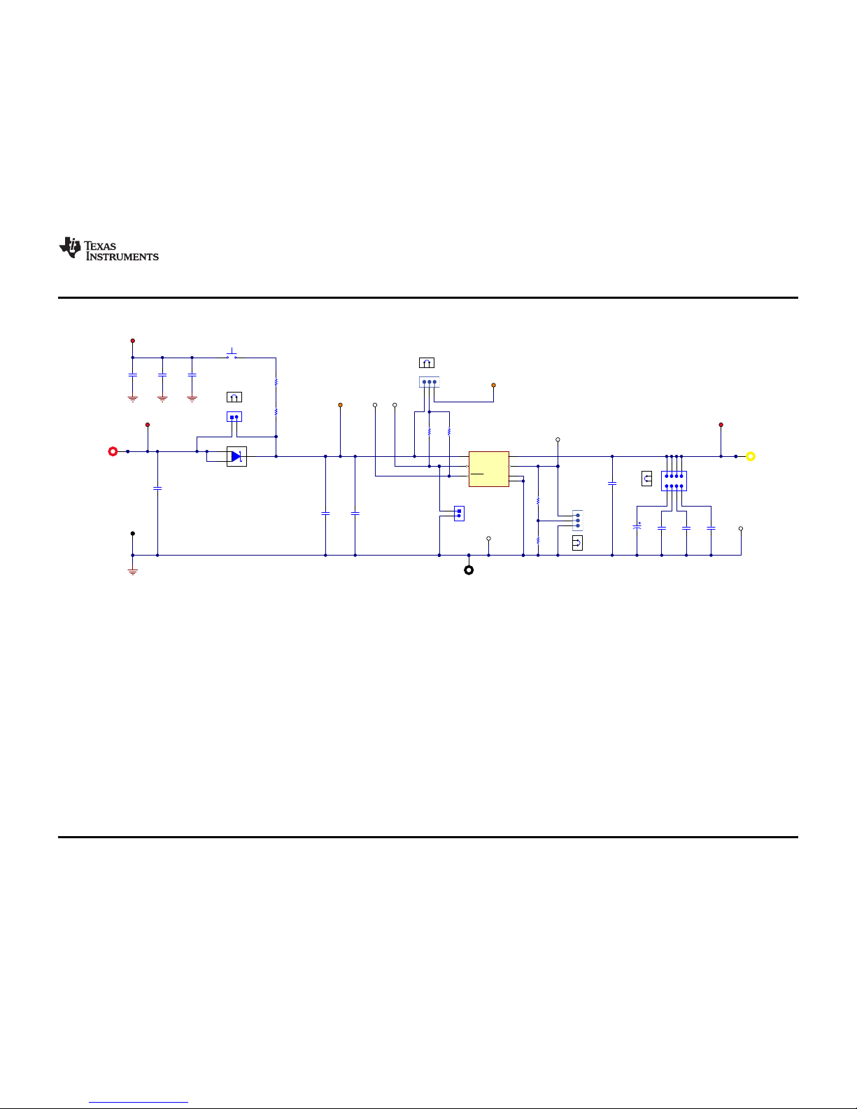
Referring to the schematic shown in Figure 1, primary input power is applied at J5/J7 while J6/J7 provides
the output connection to the load. C4/C5 provides input protection for the TPS25200 (U1) while C1 and
the J4 selectable output capacitance provide output protection. J3 allows three levels of current limit to be
selected. J2 allows selection of the EN/FAULTx pullup voltage source to come from either the IN or an
external source (VCC_IO source from TP11).
The overvoltage protection feature of the TPS25200 device can be evaluated through the use of a
secondary (higher voltage) source connected to TP10. The effects of this overvoltage pulse can be
evaluated by using the S1 pushbutton.
2
TPS25200EVM-618 Evaluation Module for TPS25200 SLVUA53A–March 2014–Revised April 2014
Copyright © 2014, Texas Instruments Incorporated
Submit Documentation Feedback
Page 3
J7
J5
J6
TP4
TP8
TP6
TP1
TP3
TP7
TP9
ILIM
IN
COMMON GROUND
VIN
EN
ENABLE
1
2
3
J3
ILIM LO
ILIM HI
VOUT
VIN = 2.5 to 6.5 V
IIN = 75 mA to 2.5 A
VOUT = 2.5 to 5.4 V
IOUT = 75 mA to 2.5A
TP2
FLTx
TP5
S1
1
2
J1
10 µF
C2
10 µF
C4
1234567
8
J4
1
2
J8
332 kΩ
R3
332 kΩ
R2
10 µF
C7
47 µF
C9
22 µF
C8
OUT
1
ILIM
2
FAULT
3
EN
4
GND
5
IN
6
PAD
U1
TPS25200DRV
100 V
D1
V8P10-M3/86A
0.1 Ω
R1
TP10
VIN 0 V
80.6 kΩ
R5
2.8 A
1.1 A
OVP VIN (20 V Max)
OVP TEST
123
J2 VCC IO (7 V Max)
TP11
SH-J2
SH-J4
SH-J3
SH-J1
D1 SHORT
COUT
47 µF
C11
47 µF
C10
47 µF
C3
0.2 Ω
R6
0.1 µF
C1
0.1 µF
C5
IN
EN
FLTx
OUT
ILIM
33.2 kΩ
R4
150 µF
C6
www.ti.com
Schematic
3 Schematic
Figure 1. TPS25200EVM-618 Schematic
3
SLVUA53A–March 2014–Revised April 2014 TPS25200EVM-618 Evaluation Module for TPS25200
Submit Documentation Feedback
Copyright © 2014, Texas Instruments Incorporated
Page 4
General Configuration and Description
4 General Configuration and Description
4.1 Physical Access
Table 1 lists the TPS25200EVM-618 connector functionality, Table 2 describes the test point availability,
and Table 3 describes the jumper functionality.
Table 1. Connector Functionality
Connector Label Description
J5/J7 VIN/GND 2.5- to 6.5-V primary input to the EVM
TP10 VIN_OV 2.5- to 20-V HV test voltage input to the EVM
J6/J7 VOUT/GND 2.5- to 5.4-V output from the EVM
S1 S1 S1 is used to pulse test the OVP feature
Table 2. Test Points
Test Point Color Label Description
TP4/TP8/TP7 RED/BLK/SM VIN/GND 2.5- to 6.5-V primary input to the EVM
TP6/TP9 RED/SM VOUT/GND 2.5- to 5.4-V output from the EVM
TP5 ORG IN 2.5- to 6.5-V input to the TPS25200
TP11 ORG VCC IO 2.5- to 6.5-V pullup source for EN and FAULTx
TP1 WHT EN Active high enable input
TP2 WHT FLT Fault test point
TP3 WHT ILIM TPS25200 ILIM pin voltage
www.ti.com
Table 3. Jumpers and LEDs
Jumper Label Description
J1 J1
J2 J2 to the IN pin. When the shunt is in the IO position, then an external IO source should be
J3 ILIM
J4 COUT Select the desired output capacitance using a shunt on J4 per the schematic diagram.
J8 EN Remove the shunt to enable the TPS25200 and install the shunt to disable.
Install between pins 1 and 2 to short out D1 (for normal operation). Remove when testing the
OVP feature using S1.
Select the desired EN and FLT pullup resistor supply source using a shunt on J2 per the
schematic diagram. When the shunt is in the IN position, then the pullup source is connected
connected between TP11 and J7 (or another GND test point). For extended high voltage
pulse testing, use the IO position with a supply voltage below 7 V.
Select the desired current limit using a shunt on J3 per the schematic diagram. When the
shunt is removed, the current limit is approximately 850 mA.
4
TPS25200EVM-618 Evaluation Module for TPS25200 SLVUA53A–March 2014–Revised April 2014
Copyright © 2014, Texas Instruments Incorporated
Submit Documentation Feedback
Page 5
Positive
Voltmeter
PRINT
HELP
ALPHA
SHIFT
ENTER
RUN
DGERF
I
AJBKC
L
7M8N9
O
DGDGD
G
D
G T3U
0V.WX
Y
Z
TAB
% UTILIZATION
HUB/MAU NIC
2
BNC
4Mb/s
Oscilloscope
Power
Supply
Negative
DUT
PWR618
J5 J6
J7
J3
S1
Positive
Load
Negative
HI
LO
Positive
TP4
TP5
TP6
TP8
TP9
TP2
TP7
TP10
www.ti.com
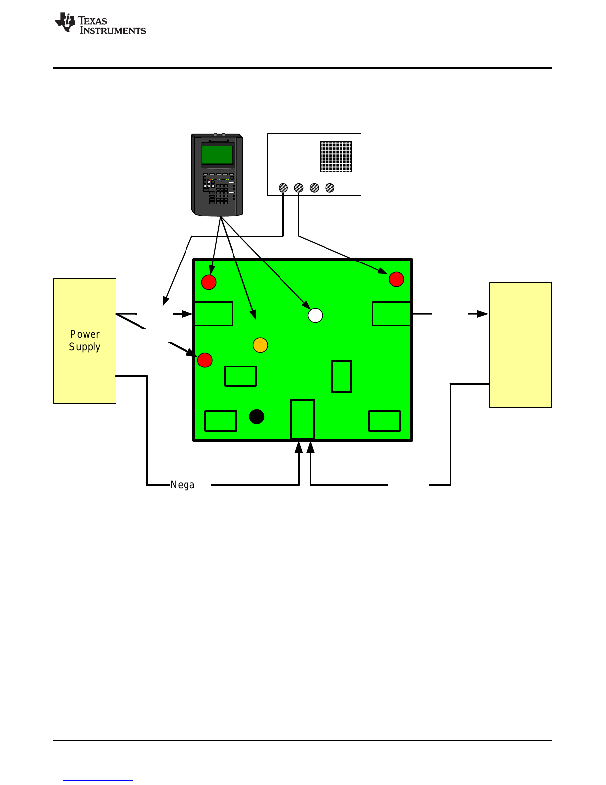
4.2 Test Setup
Figure 2 shows a typical test setup for TPS25200EVM-618. Connect J5 to the primary power supply,
TP10 to the HV power supply, and J6 to the load. J7 is the common return for J5, J6, and TP10.
General Configuration and Description
Figure 2. Typical TPS25200EVM-618 Test Setup
SLVUA53A–March 2014–Revised April 2014 TPS25200EVM-618 Evaluation Module for TPS25200
Submit Documentation Feedback
5
Copyright © 2014, Texas Instruments Incorporated
Page 6

EVM Assembly Drawings and Layout Guidelines
5 EVM Assembly Drawings and Layout Guidelines
The following PCB drawings show component placement and layout of the EVM.
Figure 3. Top Side Placement
www.ti.com
6
TPS25200EVM-618 Evaluation Module for TPS25200 SLVUA53A–March 2014–Revised April 2014
Figure 4. Top Side Routing
Figure 5. Bottom Side Routing
Copyright © 2014, Texas Instruments Incorporated
Submit Documentation Feedback
Page 7

www.ti.com
6 Bill of Materials
Bill of Materials
Table 4. TPS25200EVM-618 Bill of Materials
Designator QTY Value Description Part Number Manufacturer Number –
!PCB 1 Printed Circuit Board PWR618 Any -
C1, C5 1 0.1uF 0805 08055C104KAT2A AVX
C2, C4 2 10uF 0805 TDK
C3, C10, CAP, CERM, 47uF, 25V, ±20%, C3216X5R1E476M
C11 X5R, 1206 160AC
C6 1 150uF 7343-31 Kemet
C7 1 10uF 0805 0805YD106MAT2A AVX
C8 1 22uF 1206 1206YD226MAT2A AVX
C9 1 47uF 1206 TDK
D1 1 100V TO-277A V8P10-M3/86A
FID1, FID2, Fiducial mark. There is nothing to
FID3 buy or mount.
H1, H2, H3, Bumpon, Cylindrical, 0.312 X
H4 0.200, Black
J1, J8 2 2x1 Header TSW-102-07-G-S Samtec
J2, J3 2 1x3 PBC03SAAN PBC03SAAN Connector
J4 1 4x2 Header TSW-104-07-G-D Samtec
J5 1 10A 571-0500 571-0500
J6 1 10A 571-0700 571-0700
J7 1 10A 571-0100 571-0100
LBL1 1 Labels, 1.250" W x 0.250" H - 1.25"H x THT-13-457-10 Brady
R1 1 0.1 RES, 0.1 ohm, 1%, 0.5W, 2010 2010 Vishay-Dale
R2, R3 2 332k RES, 332k ohm, 1%, 0.1W, 0603 0603 Vishay-Dale
R4 1 33.2k 0805 Vishay-Dale
R5 1 80.6k 0805 Vishay-Dale
R6 1 0.2 RES, 0.2 ohm, 1%, 0.5W, 2010 2010 Vishay-Dale
S1 1 Switch, Push Button, SMD SKRKAEE010 Alps
SH-J1, SH- Sullins
J2, SH-J3, 4 1x2 Shunt, 100mil, Flash Gold, Black SPC02SYAN Connector
SH-J4 Solutions
(1)
Unless otherwise noted in the Alternate Part Number – Manufacturer column, all parts may be substituted with equivalents.
3 47uF 1206 TDK
0 Fiducial N/A N/A
4 Black Bumpon SJ61A1 3M
CAP, CERM, 0.1uF, 50V, ±10%,
X7R, 0805
CAP, CERM, 10uF, 25V, ±10%, C2012X5R1E106K
X5R, 0805 125AB
CAP, TA, 150uF, 16V, ±10%, T495D157K016AT
0.125 ohm, SMD E125
CAP, CERM, 10uF, 16V, ±20%,
X5R, 0805
CAP, CERM, 22uF, 16V, ±20%,
X5R, 1206
CAP, CERM, 47uF, 16V, ±15%, C3216X5R1C476M
X5R, 1206 160AB
Diode, Schottky, 100V, 8A, TO- Vishay-
277A Semiconductor
Header, TH, 100mil, 2x1, Gold
plated, 230 mil above insulator
Header, TH, 100mil, 1x3, Gold Equivalent –
plated, 230 mil above insulator Any
Header, TH, 100mil, 4x2, Gold
plated, 230 mil above insulator
Standard Banana Jack, DEM Equivalent –
insulated, 10A, red Manufacturing Any
Standard Banana Jack, DEM Equivalent –
insulated, 10A, yellow Manufacturing Any
Standard Banana Jack, DEM Equivalent –
insulated, 10A, black Manufacturing Any
Thermal Transfer Printable PCB Label
10,000 per roll 0.250"W
RES, 33.2k ohm, 1%, 0.125W, CRCW080533K2F
0805 KEA
RES, 80.6k ohm, 1%, 0.125W, CRCW080580K6F
0805 KEA
Package
Reference
WSL2010R1000FE Equivalent –
A Any
CRCW0603332KF
KEA
WSL2010R2000FE
A
2.9x2x3.9mm Equivalent –
SMD Any
Closed Top
100mil Shunt
(1)
Alternate Part
Manufacturer
Sullins
Solutions
SLVUA53A–March 2014–Revised April 2014 TPS25200EVM-618 Evaluation Module for TPS25200
Submit Documentation Feedback
7
Copyright © 2014, Texas Instruments Incorporated
Page 8
Bill of Materials
www.ti.com
Table 4. TPS25200EVM-618 Bill of Materials
Designator QTY Value Description Part Number Manufacturer Number –
TP1, TP2, Test Point, TH, Multipurpose, Equivalent –
TP3 White Any
TP4, TP6, Test Point, TH, Multipurpose, Equivalent –
TP10 Red Any
TP5, TP11 2 Orange Keystone5013 5013 Keystone
TP7, TP9 2 SMT Test Point, SMT, Compact 5016 Keystone
TP8 1 Black Keystone5011 5011 Keystone
U1 1 DRV0006A TPS25200DRV None
3 White Keystone5012 5012 Keystone
3 Red Keystone5010 5010 Keystone
Test Point, TH, Multipurpose, Equivalent –
Orange Any
Test Point, TH, Multipurpose, Equivalent –
Black Any
Precision Adjustable CurrentLimited Power Distribution Switch Texas
with Overvoltage Protection, Instruments
DRV0006A
Package
Reference
Testpoint_Keyst Equivalent –
one_Compact Any
(1)
(continued)
Alternate Part
Manufacturer
8
TPS25200EVM-618 Evaluation Module for TPS25200 SLVUA53A–March 2014–Revised April 2014
Copyright © 2014, Texas Instruments Incorporated
Submit Documentation Feedback
Page 9

www.ti.com
Revision History
Revision History
Changes from Original (March 2014) to A Revision ....................................................................................................... Page
• Updated C1 in Figure 1 .................................................................................................................. 3
• Updated C1 and C5 in Table 4 ......................................................................................................... 7
SLVUA53A–March 2014–Revised April 2014 Revision History
Submit Documentation Feedback
9
Copyright © 2014, Texas Instruments Incorporated
Page 10

ADDITIONAL TERMS AND CONDITIONS, WARNINGS, RESTRICTIONS, AND DISCLAIMERS FOR
EVALUATION MODULES
Texas Instruments Incorporated (TI) markets, sells, and loans all evaluation boards, kits, and/or modules (EVMs) pursuant to, and user
expressly acknowledges, represents, and agrees, and takes sole responsibility and risk with respect to, the following:
1. User agrees and acknowledges that EVMs are intended to be handled and used for feasibility evaluation only in laboratory and/or
development environments. Notwithstanding the foregoing, in certain instances, TI makes certain EVMs available to users that do not
handle and use EVMs solely for feasibility evaluation only in laboratory and/or development environments, but may use EVMs in a
hobbyist environment. All EVMs made available to hobbyist users are FCC certified, as applicable. Hobbyist users acknowledge, agree,
and shall comply with all applicable terms, conditions, warnings, and restrictions in this document and are subject to the disclaimer and
indemnity provisions included in this document.
2. Unless otherwise indicated, EVMs are not finished products and not intended for consumer use. EVMs are intended solely for use by
technically qualified electronics experts who are familiar with the dangers and application risks associated with handling electrical
mechanical components, systems, and subsystems.
3. User agrees that EVMs shall not be used as, or incorporated into, all or any part of a finished product.
4. User agrees and acknowledges that certain EVMs may not be designed or manufactured by TI.
5. User must read the user's guide and all other documentation accompanying EVMs, including without limitation any warning or
restriction notices, prior to handling and/or using EVMs. Such notices contain important safety information related to, for example,
temperatures and voltages. For additional information on TI's environmental and/or safety programs, please visit www.ti.com/esh or
contact TI.
6. User assumes all responsibility, obligation, and any corresponding liability for proper and safe handling and use of EVMs.
7. Should any EVM not meet the specifications indicated in the user’s guide or other documentation accompanying such EVM, the EVM
may be returned to TI within 30 days from the date of delivery for a full refund. THE FOREGOING LIMITED WARRANTY IS THE
EXCLUSIVE WARRANTY MADE BY TI TO USER AND IS IN LIEU OF ALL OTHER WARRANTIES, EXPRESSED, IMPLIED, OR
STATUTORY, INCLUDING ANY WARRANTY OF MERCHANTABILITY OR FITNESS FOR ANY PARTICULAR PURPOSE. TI SHALL
NOT BE LIABLE TO USER FOR ANY INDIRECT, SPECIAL, INCIDENTAL, OR CONSEQUENTIAL DAMAGES RELATED TO THE
HANDLING OR USE OF ANY EVM.
8. No license is granted under any patent right or other intellectual property right of TI covering or relating to any machine, process, or
combination in which EVMs might be or are used. TI currently deals with a variety of customers, and therefore TI’s arrangement with
the user is not exclusive. TI assumes no liability for applications assistance, customer product design, software performance, or
infringement of patents or services with respect to the handling or use of EVMs.
9. User assumes sole responsibility to determine whether EVMs may be subject to any applicable federal, state, or local laws and
regulatory requirements (including but not limited to U.S. Food and Drug Administration regulations, if applicable) related to its handling
and use of EVMs and, if applicable, compliance in all respects with such laws and regulations.
10. User has sole responsibility to ensure the safety of any activities to be conducted by it and its employees, affiliates, contractors or
designees, with respect to handling and using EVMs. Further, user is responsible to ensure that any interfaces (electronic and/or
mechanical) between EVMs and any human body are designed with suitable isolation and means to safely limit accessible leakage
currents to minimize the risk of electrical shock hazard.
11. User shall employ reasonable safeguards to ensure that user’s use of EVMs will not result in any property damage, injury or death,
even if EVMs should fail to perform as described or expected.
12. User shall be solely responsible for proper disposal and recycling of EVMs consistent with all applicable federal, state, and local
requirements.
Certain Instructions. User shall operate EVMs within TI’s recommended specifications and environmental considerations per the user’s
guide, accompanying documentation, and any other applicable requirements. Exceeding the specified ratings (including but not limited to
input and output voltage, current, power, and environmental ranges) for EVMs may cause property damage, personal injury or death. If
there are questions concerning these ratings, user should contact a TI field representative prior to connecting interface electronics including
input power and intended loads. Any loads applied outside of the specified output range may result in unintended and/or inaccurate
operation and/or possible permanent damage to the EVM and/or interface electronics. Please consult the applicable EVM user's guide prior
to connecting any load to the EVM output. If there is uncertainty as to the load specification, please contact a TI field representative. During
normal operation, some circuit components may have case temperatures greater than 60°C as long as the input and output are maintained
at a normal ambient operating temperature. These components include but are not limited to linear regulators, switching transistors, pass
transistors, and current sense resistors which can be identified using EVMs’ schematics located in the applicable EVM user's guide. When
placing measurement probes near EVMs during normal operation, please be aware that EVMs may become very warm. As with all
electronic evaluation tools, only qualified personnel knowledgeable in electronic measurement and diagnostics normally found in
development environments should use EVMs.
Agreement to Defend, Indemnify and Hold Harmless. User agrees to defend, indemnify, and hold TI, its directors, officers, employees,
agents, representatives, affiliates, licensors and their representatives harmless from and against any and all claims, damages, losses,
expenses, costs and liabilities (collectively, "Claims") arising out of, or in connection with, any handling and/or use of EVMs. User’s
indemnity shall apply whether Claims arise under law of tort or contract or any other legal theory, and even if EVMs fail to perform as
described or expected.
Safety-Critical or Life-Critical Applications. If user intends to use EVMs in evaluations of safety critical applications (such as life support),
and a failure of a TI product considered for purchase by user for use in user’s product would reasonably be expected to cause severe
personal injury or death such as devices which are classified as FDA Class III or similar classification, then user must specifically notify TI
of such intent and enter into a separate Assurance and Indemnity Agreement.
Page 11

RADIO FREQUENCY REGULATORY COMPLIANCE INFORMATION FOR EVALUATION MODULES
Texas Instruments Incorporated (TI) evaluation boards, kits, and/or modules (EVMs) and/or accompanying hardware that is marketed, sold,
or loaned to users may or may not be subject to radio frequency regulations in specific countries.
General Statement for EVMs Not Including a Radio
For EVMs not including a radio and not subject to the U.S. Federal Communications Commission (FCC) or Industry Canada (IC)
regulations, TI intends EVMs to be used only for engineering development, demonstration, or evaluation purposes. EVMs are not finished
products typically fit for general consumer use. EVMs may nonetheless generate, use, or radiate radio frequency energy, but have not been
tested for compliance with the limits of computing devices pursuant to part 15 of FCC or the ICES-003 rules. Operation of such EVMs may
cause interference with radio communications, in which case the user at his own expense will be required to take whatever measures may
be required to correct this interference.
General Statement for EVMs including a radio
User Power/Frequency Use Obligations: For EVMs including a radio, the radio included in such EVMs is intended for development and/or
professional use only in legally allocated frequency and power limits. Any use of radio frequencies and/or power availability in such EVMs
and their development application(s) must comply with local laws governing radio spectrum allocation and power limits for such EVMs. It is
the user’s sole responsibility to only operate this radio in legally acceptable frequency space and within legally mandated power limitations.
Any exceptions to this are strictly prohibited and unauthorized by TI unless user has obtained appropriate experimental and/or development
licenses from local regulatory authorities, which is the sole responsibility of the user, including its acceptable authorization.
U.S. Federal Communications Commission Compliance
For EVMs Annotated as FCC – FEDERAL COMMUNICATIONS COMMISSION Part 15 Compliant
Caution
This device complies with part 15 of the FCC Rules. Operation is subject to the following two conditions: (1) This device may not cause
harmful interference, and (2) this device must accept any interference received, including interference that may cause undesired operation.
Changes or modifications could void the user's authority to operate the equipment.
FCC Interference Statement for Class A EVM devices
This equipment has been tested and found to comply with the limits for a Class A digital device, pursuant to part 15 of the FCC Rules.
These limits are designed to provide reasonable protection against harmful interference when the equipment is operated in a commercial
environment. This equipment generates, uses, and can radiate radio frequency energy and, if not installed and used in accordance with the
instruction manual, may cause harmful interference to radio communications. Operation of this equipment in a residential area is likely to
cause harmful interference in which case the user will be required to correct the interference at its own expense.
FCC Interference Statement for Class B EVM devices
This equipment has been tested and found to comply with the limits for a Class B digital device, pursuant to part 15 of the FCC Rules.
These limits are designed to provide reasonable protection against harmful interference in a residential installation. This equipment
generates, uses and can radiate radio frequency energy and, if not installed and used in accordance with the instructions, may cause
harmful interference to radio communications. However, there is no guarantee that interference will not occur in a particular installation. If
this equipment does cause harmful interference to radio or television reception, which can be determined by turning the equipment off and
on, the user is encouraged to try to correct the interference by one or more of the following measures:
• Reorient or relocate the receiving antenna.
• Increase the separation between the equipment and receiver.
• Connect the equipment into an outlet on a circuit different from that to which the receiver is connected.
• Consult the dealer or an experienced radio/TV technician for help.
Industry Canada Compliance (English)
For EVMs Annotated as IC – INDUSTRY CANADA Compliant:
This Class A or B digital apparatus complies with Canadian ICES-003.
Changes or modifications not expressly approved by the party responsible for compliance could void the user’s authority to operate the
equipment.
Concerning EVMs Including Radio Transmitters
This device complies with Industry Canada licence-exempt RSS standard(s). Operation is subject to the following two conditions: (1) this
device may not cause interference, and (2) this device must accept any interference, including interference that may cause undesired
operation of the device.
Concerning EVMs Including Detachable Antennas
Under Industry Canada regulations, this radio transmitter may only operate using an antenna of a type and maximum (or lesser) gain
approved for the transmitter by Industry Canada. To reduce potential radio interference to other users, the antenna type and its gain should
be so chosen that the equivalent isotropically radiated power (e.i.r.p.) is not more than that necessary for successful communication.
This radio transmitter has been approved by Industry Canada to operate with the antenna types listed in the user guide with the maximum
permissible gain and required antenna impedance for each antenna type indicated. Antenna types not included in this list, having a gain
greater than the maximum gain indicated for that type, are strictly prohibited for use with this device.
Page 12

Canada Industry Canada Compliance (French)
Cet appareil numérique de la classe A ou B est conforme à la norme NMB-003 du Canada
Les changements ou les modifications pas expressément approuvés par la partie responsable de la conformité ont pu vider l’autorité de
l'utilisateur pour actionner l'équipement.
Concernant les EVMs avec appareils radio
Le présent appareil est conforme aux CNR d'Industrie Canada applicables aux appareils radio exempts de licence. L'exploitation est
autorisée aux deux conditions suivantes : (1) l'appareil ne doit pas produire de brouillage, et (2) l'utilisateur de l'appareil doit accepter tout
brouillage radioélectrique subi, même si le brouillage est susceptible d'en compromettre le fonctionnement.
Concernant les EVMs avec antennes détachables
Conformément à la réglementation d'Industrie Canada, le présent émetteur radio peut fonctionner avec une antenne d'un type et d'un gain
maximal (ou inférieur) approuvé pour l'émetteur par Industrie Canada. Dans le but de réduire les risques de brouillage radioélectrique à
l'intention des autres utilisateurs, il faut choisir le type d'antenne et son gain de sorte que la puissance isotrope rayonnée équivalente
(p.i.r.e.) ne dépasse pas l'intensité nécessaire à l'établissement d'une communication satisfaisante.
Le présent émetteur radio a été approuvé par Industrie Canada pour fonctionner avec les types d'antenne énumérés dans le manuel
d’usage et ayant un gain admissible maximal et l'impédance requise pour chaque type d'antenne. Les types d'antenne non inclus dans
cette liste, ou dont le gain est supérieur au gain maximal indiqué, sont strictement interdits pour l'exploitation de l'émetteur.
Mailing Address: Texas Instruments, Post Office Box 655303, Dallas, Texas 75265
Copyright © 2014, Texas Instruments Incorporated
spacer
Important Notice for Users of EVMs Considered “Radio Frequency Products” in Japan
EVMs entering Japan are NOT certified by TI as conforming to Technical Regulations of Radio Law of Japan.
If user uses EVMs in Japan, user is required by Radio Law of Japan to follow the instructions below with respect to EVMs:
1. Use EVMs in a shielded room or any other test facility as defined in the notification #173 issued by Ministry of Internal Affairs and
Communications on March 28, 2006, based on Sub-section 1.1 of Article 6 of the Ministry’s Rule for Enforcement of Radio Law of
Japan,
2. Use EVMs only after user obtains the license of Test Radio Station as provided in Radio Law of Japan with respect to EVMs, or
3. Use of EVMs only after user obtains the Technical Regulations Conformity Certification as provided in Radio Law of Japan with respect
to EVMs. Also, do not transfer EVMs, unless user gives the same notice above to the transferee. Please note that if user does not
follow the instructions above, user will be subject to penalties of Radio Law of Japan.
http://www.tij.co.jp
【無線電波を送信する製品の開発キットをお使いになる際の注意事項】 本開発キットは技術基準適合証明を受けておりません。 本製品の
ご使用に際しては、電波法遵守のため、以下のいずれかの措置を取っていただく必要がありますのでご注意ください。
1. 電波法施行規則第6条第1項第1号に基づく平成18年3月28日総務省告示第173号で定められた電波暗室等の試験設備でご使用いただく。
2. 実験局の免許を取得後ご使用いただく。
3. 技術基準適合証明を取得後ご使用いただく。。
なお、本製品は、上記の「ご使用にあたっての注意」を譲渡先、移転先に通知しない限り、譲渡、移転できないものとします
上記を遵守頂けない場合は、電波法の罰則が適用される可能性があることをご留意ください。
日本テキサス・インスツルメンツ株式会社
東京都新宿区西新宿6丁目24番1号
西新宿三井ビル
http://www.tij.co.jp
Texas Instruments Japan Limited
(address) 24-1, Nishi-Shinjuku 6 chome, Shinjuku-ku, Tokyo, Japan
Page 13

IMPORTANT NOTICE
Texas Instruments Incorporated and its subsidiaries (TI) reserve the right to make corrections, enhancements, improvements and other
changes to its semiconductor products and services per JESD46, latest issue, and to discontinue any product or service per JESD48, latest
issue. Buyers should obtain the latest relevant information before placing orders and should verify that such information is current and
complete. All semiconductor products (also referred to herein as “components”) are sold subject to TI’s terms and conditions of sale
supplied at the time of order acknowledgment.
TI warrants performance of its components to the specifications applicable at the time of sale, in accordance with the warranty in TI’s terms
and conditions of sale of semiconductor products. Testing and other quality control techniques are used to the extent TI deems necessary
to support this warranty. Except where mandated by applicable law, testing of all parameters of each component is not necessarily
performed.
TI assumes no liability for applications assistance or the design of Buyers’ products. Buyers are responsible for their products and
applications using TI components. To minimize the risks associated with Buyers’ products and applications, Buyers should provide
adequate design and operating safeguards.
TI does not warrant or represent that any license, either express or implied, is granted under any patent right, copyright, mask work right, or
other intellectual property right relating to any combination, machine, or process in which TI components or services are used. Information
published by TI regarding third-party products or services does not constitute a license to use such products or services or a warranty or
endorsement thereof. Use of such information may require a license from a third party under the patents or other intellectual property of the
third party, or a license from TI under the patents or other intellectual property of TI.
Reproduction of significant portions of TI information in TI data books or data sheets is permissible only if reproduction is without alteration
and is accompanied by all associated warranties, conditions, limitations, and notices. TI is not responsible or liable for such altered
documentation. Information of third parties may be subject to additional restrictions.
Resale of TI components or services with statements different from or beyond the parameters stated by TI for that component or service
voids all express and any implied warranties for the associated TI component or service and is an unfair and deceptive business practice.
TI is not responsible or liable for any such statements.
Buyer acknowledges and agrees that it is solely responsible for compliance with all legal, regulatory and safety-related requirements
concerning its products, and any use of TI components in its applications, notwithstanding any applications-related information or support
that may be provided by TI. Buyer represents and agrees that it has all the necessary expertise to create and implement safeguards which
anticipate dangerous consequences of failures, monitor failures and their consequences, lessen the likelihood of failures that might cause
harm and take appropriate remedial actions. Buyer will fully indemnify TI and its representatives against any damages arising out of the use
of any TI components in safety-critical applications.
In some cases, TI components may be promoted specifically to facilitate safety-related applications. With such components, TI’s goal is to
help enable customers to design and create their own end-product solutions that meet applicable functional safety standards and
requirements. Nonetheless, such components are subject to these terms.
No TI components are authorized for use in FDA Class III (or similar life-critical medical equipment) unless authorized officers of the parties
have executed a special agreement specifically governing such use.
Only those TI components which TI has specifically designated as military grade or “enhanced plastic” are designed and intended for use in
military/aerospace applications or environments. Buyer acknowledges and agrees that any military or aerospace use of TI components
which have not been so designated is solely at the Buyer's risk, and that Buyer is solely responsible for compliance with all legal and
regulatory requirements in connection with such use.
TI has specifically designated certain components as meeting ISO/TS16949 requirements, mainly for automotive use. In any case of use of
non-designated products, TI will not be responsible for any failure to meet ISO/TS16949.
Products Applications
Audio www.ti.com/audio Automotive and Transportation www.ti.com/automotive
Amplifiers amplifier.ti.com Communications and Telecom www.ti.com/communications
Data Converters dataconverter.ti.com Computers and Peripherals www.ti.com/computers
DLP® Products www.dlp.com Consumer Electronics www.ti.com/consumer-apps
DSP dsp.ti.com Energy and Lighting www.ti.com/energy
Clocks and Timers www.ti.com/clocks Industrial www.ti.com/industrial
Interface interface.ti.com Medical www.ti.com/medical
Logic logic.ti.com Security www.ti.com/security
Power Mgmt power.ti.com Space, Avionics and Defense www.ti.com/space-avionics-defense
Microcontrollers microcontroller.ti.com Video and Imaging www.ti.com/video
RFID www.ti-rfid.com
OMAP Applications Processors www.ti.com/omap TI E2E Community e2e.ti.com
Wireless Connectivity www.ti.com/wirelessconnectivity
Mailing Address: Texas Instruments, Post Office Box 655303, Dallas, Texas 75265
Copyright © 2014, Texas Instruments Incorporated
Page 14

Mouser Electronics
Authorized Distributor
Click to View Pricing, Inventory, Delivery & Lifecycle Information:
Texas Instruments:
TPS25200EVM-618
 Loading...