3,0 mm X 4,88 mm
Actual Size
www.ti.com
1
2
3
4
5
10
9
8
7
6
EN
VREF
PROG
TIMER
GND
VCC
SENSE
GATE
OUT
PG
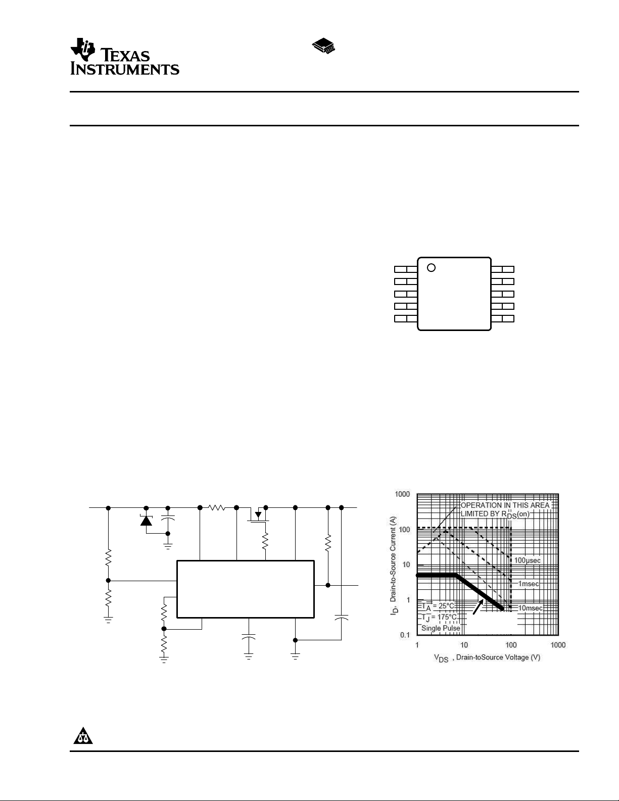
DGS Package
(Top View)
7
VCC SENSE GATE OUT
EN
VREF
PG
PROG
TIMER
GND
6
8910
1
2
3
4
5
D1
SMAJ60A
C1
0.1 µF
R
S
0.01 Ω
M1
IRF540NS
R6
470 kΩ
R5
10 Ω
R3
41.2 kΩ
R4
8.25 kΩ
C
T
0.1 µF
C
O
220 µF
R1
324 kΩ
R2
13.3 kΩ
VI = 48 Vdc
VO at 4 A
Power Good
TPS2490/91
I
LIM
= 5 A,
VON/V
OFF
= 34.2 V/31.7 V,
P
LIM
= 34 W,
Timeout = 16 mS
Programmed
SOA, 16mS
POSITIVE HIGH-VOLTAGE POWER-LIMITING HOTSWAP CONTROLLER
FEATURES APPLICATIONS
• Programmable Power Limiting and Current
Limiting for Complete SOA Protection
• Wide Operating Range: +9 V to +80 V
• Latched Operation (TPS2490) and Automatic
Retry (TPS2491)
• High-side Drive for Low-R
DS(on)
External
N-channel MOSFET
• Programmable Fault Timer to Protect the
MOSFET and Eliminate Nuisance Shutdowns
• Power Good Open-Drain Output for Downstream DC/DC Coordination
• Enable can be used as a Programmable
Undervoltage Lockout or Logic Control
• Small, Space-saving 10-pin MSOP Package
• Server Backplanes
• Storage Area Networks (SAN)
• Medical Systems
• Plug-in Modules
• Base Stations
TPS2490
TPS2491
SLVS503–NOVEMBER 2003
DESCRIPTION
The TPS2490 and TPS2491 are easy-to-use, positive high voltage, 10-pin Hot Swap Power Manager™ devices
that safely drive an external N-channel MOSFET switch. The power limit and current limit (both are adjustable
and independent of each other) ensure that the external MOSFET operates inside a selected safe operating area
(SOA) under the harshest operating conditions. Applications include inrush current limiting, electronic circuit
breaker protection, controlled load turn-on, interfacing to down-stream dc-to-dc converters, and power feed
protection. These devices are available in a small, space-saving 10-pin MSOP package and significantly reduce
the number of external devices, saving precious board space. The TPS2490/91 is supported by application
notes, an evaluation module, and a design tool.
Typical Application and Corresponding SOA
Hot Swap Power Manager is a trademark of Texas Instruments.
PRODUCTION DATA information is current as of publication date.
Products conform to specifications per the terms of the Texas
Instruments standard warranty. Production processing does not
necessarily include testing of all parameters.
Please be aware that an important notice concerning availability, standard warranty, and use in critical applications of Texas
Instruments semiconductor products and disclaimers thereto appears at the end of this data sheet.
Copyright © 2002–2003, Texas Instruments Incorporated

www.ti.com
TPS2490
TPS2491
SLVS503–NOVEMBER 2003
This integrated circuit can be damaged by ESD. Texas Instruments recommends that all integrated circuits be handled with
appropriate precautions. Failure to observe proper handling and installation procedures can cause damage.
ESD damage can range from subtle performance degradation to complete device failure. Precision integrated circuits may be more
susceptible to damage because very small parametric changes could cause the device not to meet its published specifications.
ORDERING INFORMATION
TA FUNCTION PACKAGE PART NUMBER
-40°C to 85°C
(1) Add an R suffix to the device type for tape and reel packaging.
Latched VSSOP-10 TPS2490DGS BIY
Retry (MSOP) TPS2491DGS BIX
(1)
SYMBOL
ABSOLUTE MAXIMUM RATINGS
(1)
over operating free-air temperature range (unless otherwise noted)
UNIT
Input voltage range, VCC, SENSE, EN, OUT -0.3 to 100 V
Output voltage range, GATE, PG -0.3 to 100 V
Input voltage range, PROG -0.3 to 6 V
Output voltage range, TIMER, VREF -0.3 to 6 V
Sink current, PG 10 mA
Source current, VREF 0 to 2 mA
Sink Current, PROG 2 mA
ESD - human body model 2 kV
ESD - charged device model 500 V
Maximum junction temperature, T
Storage temperature, T
Lead temperature 1.6 mm (1/16 inch) from case for 10 seconds 260 °C
(1) Stresses beyond those listed under "absolute maximum ratings" may cause permanent damage to the device. These are stress ratings
only and functional operation of the device at these or any other conditions beyond those indicated under "recommended operating
conditions" is not implied. Exposure to absolute-maximum-rated conditions for extended periods may affect device reliability
ST
J
150 °C
–65 to 150 °C
RECOMMENDED OPERATING CONDITIONS
MIN NOM MAX UNIT
V
V
I
VREF
T
T
VCC
PROG
J
A
Input voltage range 9 80 V
Input voltage range 0 4 V
Operating current range (sourcing), V
Operating junction temperature -40 125 °C
Operating free-air temperature -40 85 °C
REF
0 1 mA
DISSIPATION RATING TABLE
PACKAGE TA<25°C DERATING FACTOR TA= 70°C TA= 85°C
POWER RATING ABOVE TA= 25°C POWER RATING POWER RATING
mW (mW/°C) (mW) (mW)
VSSOP-10 (MSOP) 376 3.76 207 150
2

www.ti.com
TPS2490
TPS2491
SLVS503–NOVEMBER 2003
ELECTRICAL CHARACTERISTICS
unless otherwise noted, minimum and maximum limits apply across the recommended operating junction temperature and
voltage range, V
all outputs unloaded; positive currents are into pins.
SUPPLY CURRENT (VCC)
Enabled VEN= Hi, V
Disabled VEN= Lo, V
CURRENT SENSE INPUT (SENSE)
I
SENSE
REFERENCE VOLTAGE OUTPUT (VREF)
V
REF
POWER LIMITING INPUT (PROG)
I
PROG
R
PROG
POWER LIMITING AND CURRENT LIMITING (SENSE)
V
CL
V
SENSE
t
F_TRIP
TIMER OPERATION (TIMER)
D
RETRY
GATE DRIVE OUTPUT (GATE)
I
GATE
t
D_ON
t
D_OFF
POWER GOOD OUTPUT (PG)
V
PG_L
V
PGTL
Input bias current V
Reference voltage 0 < I
Input bias current, device enabled, sourcing or
sinking
Pulldown resistance, device disabled I
Current sense threshold V
power limiting trip V
Current sense threshold V
power limiting trip
Large overload response time to GATE low
Charge current (sourcing)
Discharge current (sinking)
TIMER upper threshold voltage 3.9 4 4.1 V
TIMER lower reset threshold voltage TPS2491 only 0.96 1.0 1.04 V
Fault retry duty cycle TPS2491 only 0.5% 0.75% 1.0%
GATE sourcing current 15 22 35 µA
GATE sinking current
GATE output voltage, V
Propagation delay: EN going true to GATE VEN= 0 → 2.5 V, 50% of VENto 50% of
output high
Propagation delay: EN going false (0 V) to
GATE output low
Propagation delay: TIMER expires to GATE
output low
Low voltage (sinking)
PG threshold voltage, V
open drain
= 0 V, and all outputs unloaded; typical specifications are at TJ= 25°C, V
TIMER
VCC
= 48 V, V
TIMER
= 0 V, and
PARAMETER TEST CONDITIONS MIN TYP MAX UNIT
= V
SENSE
SENSE
= V
SENSE
VREF
0 < V
PROG
= 200 µA, VEN= 0 V 375 600 Ω
PROG
(VCC-SENSE)
(VCC-sense)
with V
without V
(1)
PROG
PROG
PROG
V
PROG
V
(VCC-SENSE)
C
(GATE-OUT)
V
TIMER
V
TIMER
V
TIMER
V
TIMER
V
SENSE
VEN= Hi
VEN= Lo, V
VEN= Hi, V
V
(VCC-SENSE)
(GATE-OUT)
(1)
V
GATE
, V
, V
VCC
< 1 mA 3.9 4 4.1 V
< 4 V, VEN= 48 V 5 µA
= 2.4 V, V
= 0.9 V, V
= 4 V, V
SENSE
= 4 V, V
OUT
: 0 → 200 mV, 1.2 µS
= 2 nF, V
= 0 V 15.0 25.0 34.0 µA
= 0 V, TJ= 25°C 20.0 25.0 30.0 µA
= 5 V 1.50 2.5 3.70 µA
= 5 V, TJ= 25°C 2.10 2.5 3.10 µA
= V
, V
VCC
= V
GATE
= V
GATE
≥ 200 mV
= V
OUT
VCC
= V
OUT
VCC
= V
= V
VCC
= V
OUT
= 0 V or
OUT
= 30 V, V
OUT
= V
= V
SENSE
(GATE-OUT)
(GATE-OUT)
VCC
, 75 125 250 mA
VCC
, R
(GATE-OUT)
= 0 90 250 µA
OUT
VCC
= 48 V
VCC
OUT
,
= 1 V
= 7 V,
= 1 MΩ
450 1000 µA
7.5 20 µA
17 25 33 mV
45 50 55 mV
1.8 2.4 2.8 mA
12 16 V
25 40 µS
VEN= 2.5 V → 0, 50% of VENto 50% of
V
, V
= V
(1)
(1)
GATE
R
(GATE-OUT)
V
TIMER
V
TIMER
R
(GATE-OUT)
OUT
= 1 MΩ, t
: 0 → 5 V, t
to 50% of V
, 0.5 1 µS
VCC
= 1 MΩ,
< 0.1 µS
FALL
< 0.1 µS, 50% of
RISE
, V
GATE
OUT
= V
, 0.8 1 µS
VCC
IPG= 2 mA 0.1 0.25 V
IPG= 4 mA 0.25 0.5 V
rising, PG goes
OUT
V
SENSE
= V
, measure V
VCC
(VCC-OUT)
0.8 1.25 1.7 V
(1) Not tested in production.
3
www.ti.com
TPS2490
TPS2491
SLVS503–NOVEMBER 2003
ELECTRICAL CHARACTERISTICS (continued)
unless otherwise noted, minimum and maximum limits apply across the recommended operating junction temperature and
voltage range, V
all outputs unloaded; positive currents are into pins.
VPGTH V
∆V
PGT
t
DPG
OUTPUT VOLTAGE FEEDBACK INPUT (OUT)
I
OUT
ENABLE INPUT (EN)
V
EN_H
V
EN_L
INPUT SUPPLY UVLO (VCC)
PG threshold voltage, V
low
PG threshold hysteresis voltage, V
PG deglitch delay, detection to output, rising
and falling edges
Leakage current, PG false, open drain 10 µA
Bias current
Threshold, VENgoing high 1.32 1.35 1.38 V
Threshold, VENgoing low 1.22 1.25 1.28 V
VENhysteresis
Leakage current VEN= 48 V 1 µA
V
VCC
V
VCC
Hysteresis
= 0 V, and all outputs unloaded; typical specifications are at TJ= 25°C, V
TIMER
VCC
= 48 V, V
TIMER
= 0 V, and
PARAMETER TEST CONDITIONS MIN TYP MAX UNIT
falling, PG goes
OUT
(SENSE-OUT)VSENSE
(2)
(2)
= V
SENSE
V
SENSE
V
= V
OUT
V
= GND, VEN= Lo, sourcing 18 40 µA
OUT
, measure V
VCC
= V
VCC
= V
VCC
, VEN= Hi, sinking 8 20 µA
VCC
(VCC-OUT)
2.2 2.7 3.2 V
1.4 V
5 9 15 ms
100 mV
turn on Rising 8.4 8.8 V
turn off Falling 7.5 8.3 V
(2)
75 mV
(2) Not tested in production.
4
www.ti.com
200
250
300
350
400
450
500
550
600
9 19 29 39 49 59 69 79
TJ = −40C
TJ = 25C
TJ = 125C
I
VCC
− Supply Current −
VCC − Supply Voltage − V
A
45
46
47
48
49
50
51
52
53
54
55
9 19 29 39 49 59 69 79
TJ = −40C
TJ = 25C
TJ = 125C
VCC − Supply Voltage − V
− Current Limit Trip − mV
V
(
VCC − Sense)
2
2.1
2.2
2.3
2.4
2.5
2.6
9 19 29 39 49 59 69 79
TJ = −40C
TJ = 25C
TJ = 125C
− Gate Pullup Current (EN = OV) − mA
I
Gate
VCC − Supply Voltage − V
15
17
19
21
23
25
27
29
31
33
35
9 19 29 39 49 59 69 79
TJ = −40C
TJ = 25C
TJ = 125C
VCC − Supply Voltage − V
− Gate Pullup Current −
Gate
A
I
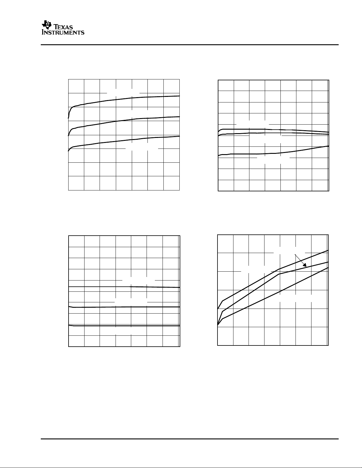
TYPICAL CHARACTERISTICS
TPS2490
TPS2491
SLVS503–NOVEMBER 2003
SUPPLY CURRENT CURRENT LIMIT TRIP
SUPPLY VOLTAGE SUPPLY VOLTAGE
GATE PULLUP CURRENT GATE PULLDOWN CURRENT(EN = 0 V)
SUPPLY VOLTAGE SUPPLY VOLTAGE
vs vs
Figure 1. Figure 2.
vs vs
Figure 3. Figure 4.
5
www.ti.com
75
95
115
135
155
175
195
215
9 19 29 39 49 59 69 79
TJ = −40C
TJ = 25C
TJ = 125C
− Gate Pulldown Current − mA
I
Gate
VCC − Supply Voltage − V
0
200
400
600
800
1000
1200
9 14 19 24 29 34 39 44 49
T − Current Limit Response Time − nS
TJ = −40C
TJ = 25C
TJ = 125C
VCC − Supply Voltage − V
18
20
22
24
26
28
30
32
9 19
29
39 49 59 69 79
− Timer Pullup Current −
TJ = −40C
TJ = 25C
TJ = 125C
I
Timer
Aµ
VCC − Supply Voltage − V
13.50
13.75
14
14.25
14.50
9 19 29 39 49 59 69 79
− Gate Output Voltage − V
TJ = −40C
TJ = 25C
TJ = 125C
VCC − Supply Voltage − V
V
Gate
TPS2490
TPS2491
SLVS503–NOVEMBER 2003
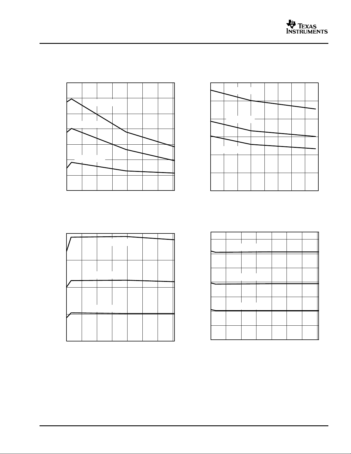
TYPICAL CHARACTERISTICS (continued)
GATE PULLDOWN CURRENT CURRENT LIMIT RESPONSE TIME
SUPPLY VOLTAGE SUPPLY VOLTAGE
(EN = 4 V, V(vcc – sense) = 200 mV) (EN = 4 V, V(vcc – sense) = 200 mV)
GATE OUTPUT VOLTAGE TIMER PULLUP CURRENT
SUPPLY VOLTAGE SUPPLY VOLTAGE
vs vs
Figure 5. Figure 6.
vs vs
6
Figure 7. Figure 8.
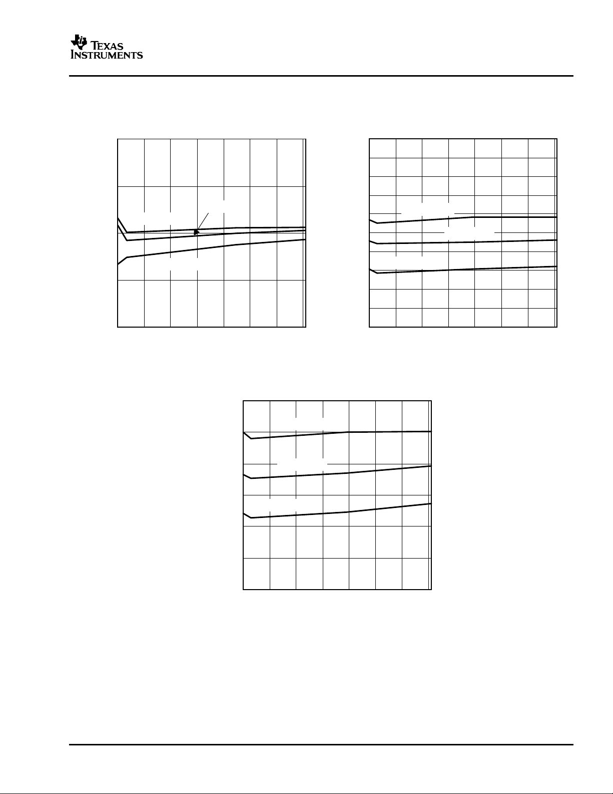
www.ti.com
9.60
9.65
9.70
9.75
9.80
9 19 29 39 49 59 69 79
TJ = −40C
TJ = 125C
TJ = 25C
− Charge/Discharge Ratio
I
Timer
VCC − Supply Voltage − V
1.245
1.246
1.247
1.248
1.249
1.250
1.251
1.252
1.253
1.254
1.255
9 19 29 39 49 59 69 79
− EN Threshold Voltage (Falling) − V
TJ = −40C
TJ = 125C
TJ = 25C
V
EN
VCC − Supply Voltage − V
1.345
1.346
1.347
1.348
1.349
1.350
1.351
9 19 29 39 49 59 69 79
TJ = −40C
TJ = 125C
TJ = 25C
− EN Threshold Voltage (Rising) − V
V
EN
VCC − Supply Voltage − V
TYPICAL CHARACTERISTICS (continued)
TPS2490
TPS2491
SLVS503–NOVEMBER 2003
TIMER CHARGE/DISCHARGE RATIO EN THRESHOLD VOLTAGE (FALLING)
SUPPLY VOLTAGE AND TEMPERATURE SUPPLY VOLTAGE
vs vs
Figure 9. Figure 10.
EN THRESHOLD VOLTAGE (RISING)
vs
SUPPLY VOLTAGE
Figure 11.
7
 Loading...