

Page 1
R
SENSEA
PGA
ENA
FLTA
SENMA
GAT1A
OUTA
SETA
GAT2A
SENPA
GND
PGB
ENB
FLTB
TPS2456
36 PIN QFN
CTB
R
SETA
INB
INA
INA
GND
GND
COMMON
CIRCUITRY
ORENB
C
INT
0.1mF
VINT
ORENA
CTA
GND
GND
GAT1B
OUTB
GAT2B
C
TB
33nF
C
TA
33nF
R
G1B
R
G2B
INB
GND
MONA
GND
GND
MONB
C
INA
0.1mF
R
G1ARG2A
R
SENSEB
SETB
SENPB
R
SETB
SENMB
R
M
O
N
C
INB
0.1mF
M1A
M2A
M1B
M2B
TPS2456
www.ti.com
Dual 12 V Protection / Blocking Controller
Check for Samples: TPS2456
1
FEATURES
• Dual 12 V Protection and Blocking Control
• Independent Current Limit and Fast Trip
• Blocking Permits ORing of Multiple Inputs
• Power Good and Fault Outputs
• Analog Current Monitor Outputs
• -40°C to 125°C Operating Junction
Temperature
• QFN36 Package
APPLICATIONS
• ATCA Carrier Boards
• AdvancedMC™ Slots
• Blade Servers
• Base Stations
• Configurable for
– 1 Source, 2 Loads
– 2 Sources, 1 Load
– 2 Sources, 2 Loads
SLVSA78A –MARCH 2010–REVISED MARCH 2010
DESCRIPTION
The TPS2456 is a dual, 12 V, channel protection
(hotswap) and blocking (ORing) controller that
provides inrush control, current limiting, overload
protection, and reverse current blocking. The current
sense topology provides both accurate current limits
and independent setting of current limit and fast trip
thresholds.
The ORing control uses an external MOSFET to
block reverse current when an input is shorted.
Systems with closely matched supply voltages and
feed networks can supply current from both supplies
simultaneously.
The MONx output provides an accurate analog
indication of load current.
The protection circuits may be used without blocking,
and the blocking may be used without protection.
Internal connections prevent implementation of these
as four fully-independent functions.
1
PRODUCTION DATA information is current as of publication date.
Products conform to specifications per the terms of the Texas
Instruments standard warranty. Production processing does not
necessarily include testing of all parameters.
Please be aware that an important notice concerning availability, standard warranty, and use in critical applications of Texas
Instruments semiconductor products and disclaimers thereto appears at the end of this data sheet.
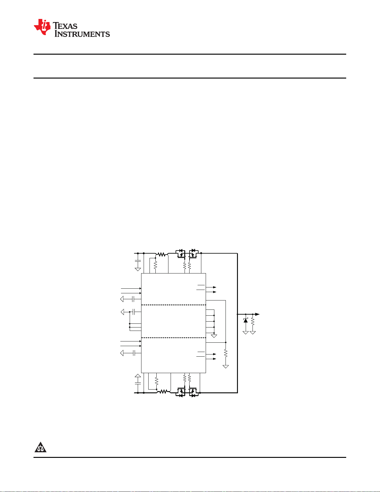
Figure 1. Two Sources, One Load Application Diagram
Copyright © 2010, Texas Instruments Incorporated
Page 2
TPS2456
SLVSA78A –MARCH 2010–REVISED MARCH 2010
www.ti.com
These devices have limited built-in ESD protection. The leads should be shorted together or the device placed in conductive foam
during storage or handling to prevent electrostatic damage to the MOS gates.
PRODUCT INFORMATION
(1)
DEVICE TEMPERATURE PACKAGE MARKING
TPS2456RHH –40°C to 85°C QFN36 (6mm × 6mm) TPS2456
(1) For package and ordering information see the Package Option Addendum at the end of this document or see the TI Web site at
www.ti.com.
THERMAL INFORMATION
TPS2456
THERMAL METRIC
q
JA
q
JC(top)
q
JB
y
JT
y
JB
q
JC(bottom)
Junction-to-ambient thermal resistance
Junction-to-case(top) thermal resistance
Junction-to-board thermal resistance
Junction-to-top characterization parameter
Junction-to-board characterization parameter
Junction-to-case(bottom) thermal resistance
(1) For more information about traditional and new thermal metrics, see the IC Package Thermal Metrics application report, SPRA953.
(2) The junction-to-ambient thermal resistance under natural convection is obtained in a simulation on a JEDEC-standard, High-K board, as
specified in JESD51-7, in an environment described in JESD51-2a.
(3) The junction-to-case(top) thermal resistance is obtained by simulating a cold plate test on the package top. No specific JEDEC-standard
test exists, but a close description can be found in the ANSI SEMI standard G30-88.
(4) The junction-to-board thermal resistance is obtained by simulating in an environment with a ring cold plate fixture to control the PCB
temperature, as described in JESD51-8.
(5) The junction-to-top characterization parameter, yJT, estimates the junction temperature of a device in a real system and is extracted
from the simulation data for obtaining qJA, using a procedure described in JESD51-2a (sections 6 and 7).
(6) The junction-to-board characterization parameter, yJBestimates the junction temperature of a device in a real system and is extracted
from the simulation data for obtaining qJA, using a procedure described in JESD51-2a (sections 6 and 7).
(7) The junction-to-case(bottom) thermal resistance is obtained by simulating a cold plate test on the exposed (power) pad. No specific
JEDEC standard test exists, but a close description can be found in the ANSI SEMI standard G30-88.
(1)
RHH UNITS
36 PINS
(2)
(3)
(4)
(5)
(6)
(7)
32
23
11
0.5
10
2.1
°C/W
ABSOLUTE MAXIMUM RATINGS
(1)
Over recommended junction temperature range and all voltages referenced to GND, unless otherwise noted.
PINS OR PIN GROUPS VALUE UNITS
GAT1x, GAT2x –0.3 to 30 V
INx, OUTx, SENPx, SENMx, SETx, ENx, FLTx, PGx, ORENx –0.3 to 17 V
CTx, MONx –0.3 to 5 V
FLTx, PGx current sinking 5 mA
MONx current sourcing 5 mA
VINT current –1 to 1 mA
ESD
Junction Temperature Internally Limited °C
(1) Stresses beyond those listed under absolute maximum ratings may cause permanent damage to the device. These are stress ratings
only. Functional operation of the device under any conditions beyond those indicated under recommended operating conditions is not
implied. Exposure to absolute maximum rated conditions for extended periods of time may affect device reliability.
2 Submit Documentation Feedback Copyright © 2010, Texas Instruments Incorporated
Human Body Model 2 kV
Charged Device Model 0.5 kV
Product Folder Link(s): TPS2456
Page 3
TPS2456
www.ti.com
SLVSA78A –MARCH 2010–REVISED MARCH 2010
RECOMMENDED OPERATING CONDITIONS
Over recommended junction temperature range and all voltages referenced to GND, unless otherwise noted.
MIN TYP MAX UNIT
V
INx
I
MONx
GAT1x, GAT2x board leakage current
(1)
VINT bypass capacitance 1 100 250 nF
Operating junction temperature range, T
J
(1) This condition applies to the PCB and is not a limit on the TPS2456.
8.5 12 15 V
100 1000 µA
–1 1 µA
–40 125 °C
ELECTRICAL CHARACTERISTICS
Common conditions (unless otherwise noted) are: INA = INB = SENPA = SENPB = SENMA = SENMB = SETPA = SETPB =
12 V, ENA = ENB = ORENA = ORENB = 3 V, CTA = CTB = GND, R
–40°C ≤ TJ≤ 125°C
PARAMETER TEST CONDITIONS MIN TYP MAX UNIT
Enable Input – ENx, ORENx
Threshold voltage V
Hysteresis 20 50 80 mV
Pullup current ENx = ORENx = 0 V, current sourcing 5 8 15 µA
Input bias current ENx = ORENx = 17 V, current sinking 6 15 µA
Turn off time
(1) (2)
Power Good Output – PGx
Output low voltage I
Leakage current PGx = 17 V (sinking) 1 µA
Threshold voltage PGx, V
Hysteresis PGx, V
Deglitch time PGx falling 50 100 150 µs
Fault Output – FLTx
Output low voltage I
Leakage current V
Bias Supply – VINT
Output voltage 0 < I
Fault Timer – CTx
Sourcing current V
Upper threshold voltage 1.30 1.35 1.40 V
Discharge pulldown
(2)
Timer start threshold 5 6 7 V
Channel Current Monitor – MONx
Input referred offset –1.5 1.5 mV
MONx threshold V
Leakage current V
(1) Tested with HAT2156 MOSFET.
(2) These parameters are provided for reference only, and do not constitute part of TI's published device specifications for purposes of TI's
product warranty.
↑ 1.25 1.35 1.45 V
INx
ENx deasserts to V
= 2 mA sinking 0.14 0.25 V
PGx
↓ 10.2 10.5 10.8 V
OUTx
↑ 130
OUTx
= 2 mA sinking 0.14 0.25 V
FLTx
= 17 V (sinking) 1 µA
FLTx
< 50 µA 2 2.3 2.8 V
VINT
= 0 V, during fault 7 10 13 µA
CTx
(V
– V
GAT1x
current
10.8 V ≤ V
measure V
GAT1x
SETx
) when timer starts, with V
INx
SENMx
– V
SETx
= 15 V 0.66 0.675 0.69 V
= (V
SENMx
< 1 V, C
OUTx
≤ 13.2 V, V
SENMx
SENPx
OUT
= V
= 0 µF, Q
GAT1x
+ 50 mV,
SENMx
– 10 mV) 1 µA
= R
MONA
= 33 nF 20 µs
GAT1x
= 6.81kΩ, all other pins open,
MONB
(2)
200 Ω
falling due to over
mV
Copyright © 2010, Texas Instruments Incorporated Submit Documentation Feedback 3
Product Folder Link(s): TPS2456
Page 4
V
T
90%
V
ENx
V
GAT1x
,
V
GAT2x
t
P50-90
time
50%
V
SENPx
-
V
SENMx
V
GAT1x
,
V
GAT2x
t
P50-50
time
50%
TPS2456
SLVSA78A –MARCH 2010–REVISED MARCH 2010
www.ti.com
ELECTRICAL CHARACTERISTICS (continued)
Common conditions (unless otherwise noted) are: INA = INB = SENPA = SENPB = SENMA = SENMB = SETPA = SETPB =
12 V, ENA = ENB = ORENA = ORENB = 3 V, CTA = CTB = GND, R
–40°C ≤ TJ≤ 125°C
PARAMETER TEST CONDITIONS MIN TYP MAX UNIT
Current limit
R
= 500 Ω, R
Current limit threshold 47.5 50 52.5 mV
Sink current in current
limit
Fast trip threshold Measure V
Fast turn-off delay (V
SETx
V
GAT1x
V
MONx
SENP
= 15 V
= 1 V, V
SENPx
– V
SENM
Channel UVLO
UVLO V
UVLO hysteresis V
↑ 8.1 8.5 8.9 V
INx
↓ 0.44 0.5 0.59 V
INx
Blocking Comparator
Turn-on threshold Measure (V
Turn-off threshold Measure (V
SENPx
SENPx
Turn-off delay 20 mV overdrive, t
Gate Drivers – GAT1x, GAT2x
Output voltage V
Sourcing current V
Sinking current
= V
INx
= V
INx
Fast turnoff, V
= 10 V 21.5 23 24.5 V
OUTx
= 10 V, V
OUTx
GAT1x
Sustained, 4 V ≤ (V
Pulldown resistance In thermal shutdown 14 20 26 kΩ
Fast turn-off duration 5 10 15 µs
Disable delay ENx pin to V
GATx1
Startup Time INx rising to GAT1x or GAT2x sourcing current (ENx and ORENx 0.25 ms
high)
Supply Current (I
INx
+ I
SENPx
+ I
SENMx
+ I
SETx
Both channels enabled 3.1 4 mA
Both channels disabled 2 2.8 mA
Thermal Shutdown
Shutdown temperature TJrising 140 150 °C
Hysteresis 10
(3) See Figure 3 for timing definition.
(4) See Figure 2 for timing definition.
(5) These parameters are provided for reference only, and do not constitute part of TI's published device specifications for purposes of TI's
product warranty.
= 6800 Ω, measure V
MONx
= 12 V, measure I
GAT1x
– V
SENMx
): 0 V → 120 mV, t
– V
) 5 10 20 mV
OUTx
– V
) –6 –3 0 mV
OUTx
p50-50
= V
GAT1x
+ I
= V
GAT1x
and V
OUTx
= 14 V, pulsed measurement 0.5 1 A
GAT2x
= V
GAT2x
, t
GAT2x
)
SENPx
GAT1x
(3)
P50-50
= 17 V 20 30 40 µA
GAT2x
) ≤ 25 V 10 14 20 mA
(4)
P50-90
MONA
– V
= R
SENMx
= 6.81kΩ, all other pins open,
MONB
when
20 40 µA
80 100 120 mV
200 300 ns
200 300 ns
1 µs
(5)
°C
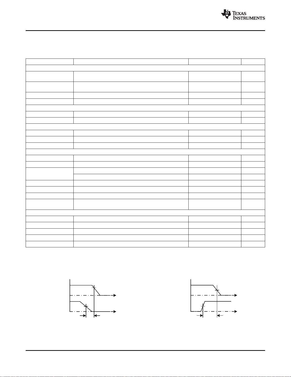
Figure 2. t
4 Submit Documentation Feedback Copyright © 2010, Texas Instruments Incorporated
Definition Figure 3. t
P50-90
Product Folder Link(s): TPS2456
P50-50
Definition
Page 5
+
+
+
100mV
675mV
Control
& Fault
Vcp
30mA
enx
C
Tx
R
MONx
FLTx
PGx
prgx
blx
OUTx
GAT2x
GAT1x
SETx
SENMx
SENPx
100ms
INx
OUTx
10.50V /
10.63V
+
30mA
ENx
MONx
CTx
por
Charge
Pump
Vcp
~25V
60mA
ORENx
R
G1x
R
SETx
R
G2x
A
2
A
1
R
SENSEx
M
1
M
2
+
+
10 mV
3 mV
SQQ
R
OUTx
prgx
blx
200kW
VINT
2
0
0
k
W
VINT
enx
12V Channel
Input Supply
8.5V
/ 8V
+
+
6V
INx
Fast
Trip
Current
Limit
FLT Tmr.
Gate Mon.
10ms
UVLO
Blocking
Control
Output
PG
10ms
PREREG
VINT
2.2V
Pwr On
Reset
en por
Control
Logic
GND
INA
INB
OUTA
OUTB
+
VINT
C
VINT
TPS2456
www.ti.com
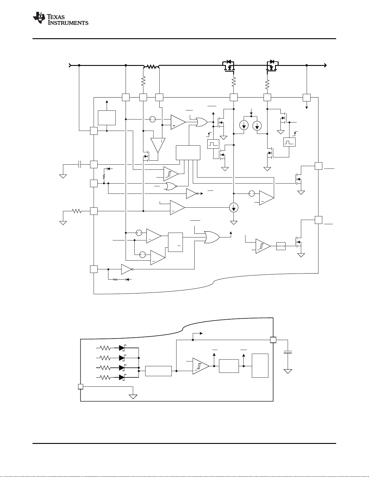
FUNCTIONAL BLOCK DIAGRAM
SLVSA78A –MARCH 2010–REVISED MARCH 2010
Figure 4. TPS2456 Channel (2 channels per device)
Figure 5. Common Control Circuits
Copyright © 2010, Texas Instruments Incorporated Submit Documentation Feedback 5
Product Folder Link(s): TPS2456
Page 6
TPS2456
SLVSA78A –MARCH 2010–REVISED MARCH 2010
PIN FUNCTIONS
PIN
NAME NO.
TYPE A/B
SENPA 1 I A Input voltage sense – connect to input supply. Connect to the source side of R
SETA 2 I A
SENMA 3 I A Connect this pin to the load side of the R
VINT 4 I/O – Connect a bypass capacitor (e.g., 0.01µF) to GND for this internal supply.
MONA 5 I/O A
ORENA 6 I A Blocking transistor enable, active high.
GND 7 GND – Connect pin to ground.
GND 8 GND – Connect pin to ground
MONB 9 I/O B
CTB 10 I/O B Connect CTBfrom CTB to GND to set the fault timer period (see text).
GAT2B 11 O B Blocking transistor gate drive.
OUTB 12 I/O B Output voltage monitor and bias input.
GND 13 GND B Connect pin to ground.
ORENB 14 I B Blocking transistor enable, active high.
GAT1B 15 O B Protection transistor gate drive.
SENMB 16 I B Connect this pin to the load side of the R
SETB 17 I B
SENPB 18 I B Input voltage sense – connect to input supply. Connect to the source side of R
INB 19 PWR B Control power input – connect to input supply.
– 20 – – No connection.
FLTB 21 O B Fault output, active low, asserted when B fault timer runs out.
PGB 22 O B Power good output, active low, asserts when V
GND 23 GND – Connect pin to ground.
GND 24 GND – Connect pin to ground.
GND 25 GND – Connect pin to ground.
PGA 26 O A Power good output, active low, asserts when V
FLTA 27 O A Fault output, active low, asserted when A fault timer runs out.
GND 28 GND – Connect pin to ground.
ENB 29 I B Enable, (active high).
GAT1A 30 O A Protection transistor gate drive.
ENA 31 I A Enable, (active high).
GND 32 GND A Connect pin to ground.
OUTA 33 I/O A Output voltage monitor and bias input.
GAT2A 34 O A Blocking transistor gate drive.
CTA 35 I/O A Connect CTAfrom CTA to GND to set the fault timer period (see text).
INA 36 PWR A Control power input – connect to input supply.
PAD – – – Solder pad to GND.
(1) Specifies whether this pin is part of A channel, B channel, or is common to both (-).
(1)
Connect R
and R
MONA
Connect R
text).
Connect R
text).
Connect R
conjunction with R
DESCRIPTION
from the input supply to SETA to program the current limit in conjunction with R
SETA
(see text).
. The fast-trip threshold equals 100 mV / R
SENSEA
from MONA to GND to set the current limit in conjunction with R
MONA
from MONB to GND to set the current limit in conjunction with R
MONB
. The fast-trip threshold equals 100 mV / R
SENSEB
from input supply to SETB to program the current limit program the current limit in
SETB
SENSEB
and R
MONB
(see text).
OUTB
OUTA
> 10.63 V.
> 10.63 V.
SENSEA
SENSEA
SENSEB
SENSEB
.
.
SENSEA
and R
and R
SENSEB
www.ti.com
SENSEA
.
(see
SETA
(see
SETB
.
6 Submit Documentation Feedback Copyright © 2010, Texas Instruments Incorporated
Product Folder Link(s): TPS2456
Page 7
TPS2456
1
3
2
4
6
5
7
9
8
27
25
26
24
22
23
21
19
20
36 3435 33 3132 30 2829
10 1211 13 1514 16 1817
SENPA
SETA
SENMA
VINT
MONA
ORENA
GND
GND
MONB
FLTA
PGA
GND
GND
GND
PGB
FLTB
NC
INB
INA
CTA
GAT2A
OUTA
GND
ENA
GAT1A
ENB
GNDSENPB
SETB
SENMB
GAT1B
ORENB
GND
OUTB
GAT2B
CTB
PAD - Backside
TPS2456
www.ti.com
SLVSA78A –MARCH 2010–REVISED MARCH 2010
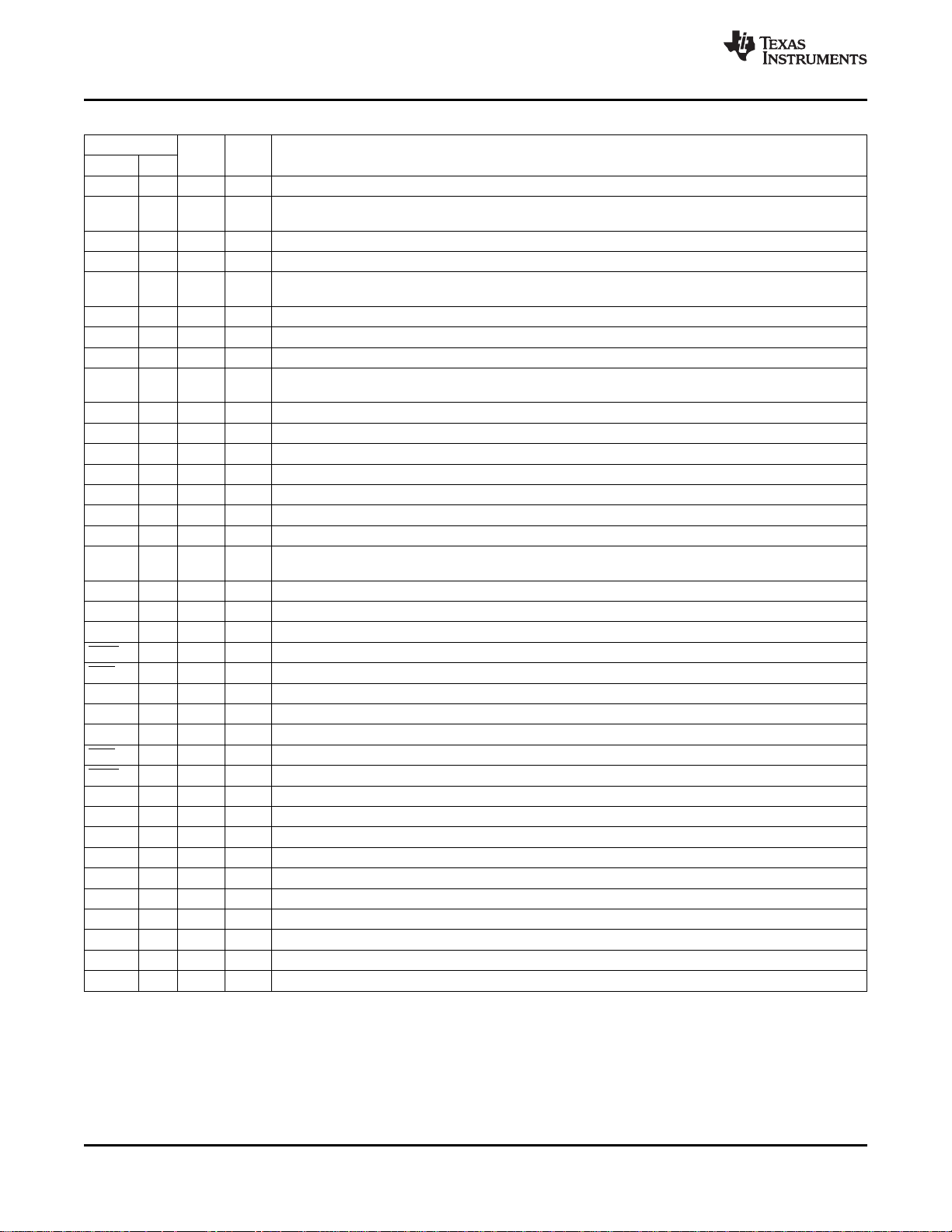
DEVICE PINOUT
(TOP VIEW)
DETAILED PIN DESCRIPTIONS
The TPS2456 supports two 12-V protection (hotswap) and blocking (ORing) channels designated A and B.
Where there are separate pins for both A and B channels, the pin name is shown with an x in place of A or B to
describe the function. For example, references to CTx would be the same as CTA or CTB. Programming
components are referred to in the text by reference designators used in Figure 1.
CTx – A capacitor from CTx to GND sets the period V
channel down and declares a fault. V
will be low during startup and current limit. Low V
GAT1x
to source 10 µA into the external capacitor (CTx). When V
by pulling the GAT1x and GAT2x pins low, declares a fault by pulling the FLTx pin low, and latching off. A 200 Ω
internal pull down keeps this pin low during normal operation when not in current limit. It is normal to see a
sawtooth on this pin when the channel is latched off by a fault.
ENx – Active high enable input. A low on ENx turns off the channel by pulling GAT1x and GAT2x low. An internal
200 kΩ resistor pulls this pin up to VINT. ENx may be left floating when the channel is to be permanently
enabled.
FLTx – Active low open-drain output indicating that V
the fault timer and shut the channel down. FLTx may be left open if not used.
GAT1x – Gate drive output for the protection MOSFET. This pin sources 30 µA to turn the MOSFET on. An
internal clamp prevents this pin from rising more than 14.5 V above INx.
Up to 30µA may be sunk while current limit is active. A fast trip (overcurrent), disable (from ENx), or fault timeout
enables a 10 µs, 1 A, discharge current and 14 mA pulldown. The pulldown will be released after 10 µs if only a
fast trip had occurred.
Setting ENx low holds GAT1x low. GAT1x may be left open if not used.
Copyright © 2010, Texas Instruments Incorporated Submit Documentation Feedback 7
Product Folder Link(s): TPS2456
can be low ( V
GAT1x
reaches 1.35 V, the TPS2456 shuts the channel off
CTx
has been low ( V
GAT1x
GAT1x
GAT1x
< V
+ 6 V) before it shuts the
INx
GAT1x
< V
+ 6 V) long enough trip
INx
causes this pin
Page 8

TPS2456
SLVSA78A –MARCH 2010–REVISED MARCH 2010
www.ti.com
GAT2x – Gate drive output for the blocking MOSFET. The blocking MOSFET prevents reverse channel current
when OUTx is higher than INx. This is often used when two input sources are ORed together. GAT2x sources 30
µA to turn the MOSFET on. GAT2x is low when ENx is low, ORENx is low, FLTx is low, a fast trip is active, or a
voltage reversal has occurred. A 10 µs, 1 A, discharge and 14 mA pulldown are applied when this occurs.
An internal clamp prevents this pin from rising more than 14.5 V above OUTx. Setting the ORENx or ENx pins
low holds the GAT2x pin low.
GAT2x may be left open if not used.
INx - Supply pin for the internal circuitry. A small bypass capacitor (e.g. 0.1 µF) is recommended for this pin.
MONx – A resistor connected from this pin to ground forms part of the current limit programming. As the current
delivered to the load increases, so does the voltage on this pin. The current-limit circuit controls GAT1x to limit
channel current at a V
Equation 1 through Equation 4 define current limit and fast trip values using R
of 675 mV. The current limit circuit is inactive for lower values of V
MONx
MONx
, R
SENSEx
.
MONx
, and R
SETx
. V
MONx
can by sampled with an external A/D converter to measure the channel current.
ORENx – Active high input. Pulling this pin low disables the blocking function by pulling the GAT2x pin low.
Pulling this pin high (or allowing it to float high) allows the blocking function to operate normally. The M2x internal
diode may carry the load current when GAT2x is low and V
INX
> V
OUTX
.
An internal 200 kΩ resistor pulls this pin to VINT. ORENx may be left open when blocking is not used, or does
not require active control.
OUTx – Senses the output voltage of the channel. This voltage is used by the biasing, blocking, and power good
circuits.
PGx – Active low open-drain output. A low on PGx indicates that V
has exceeded 10.63 V, and has not
OUTx
fallen below 10.50 V. These thresholds are internally set, and modifying the OUTx connection may effect
blocking operation.
SENMx – Senses the voltage on the load side of R
SENSEx
SENPx – Senses the voltage on the source side of R
trip overcurrent shutdown is activated at a V
SENP-SENM
SETx – A resistor connected from this pin to SENPx sets the current limit level in conjunction with R
R
as described in Equation 1 through Equation 4.
MONx
for use by the fast trip and current limiting circuits.
SENSEx
for use by the fast trip and blocking circuits. The fast
of 0.1 V.
SENSEx
and
VINT – This pin connects to the internal 2.35 V rail. A 0.1 µF capacitor must be connected from this pin to
ground. VINT is not designed to be a general-purpose bias rail.
8 Submit Documentation Feedback Copyright © 2010, Texas Instruments Incorporated
Product Folder Link(s): TPS2456
Page 9
2
2.1
2.2
2.3
2.4
-40 -20 0 20 40 60 80 100 120
T -JunctionTemperature-°C
J
SupplyCurrent-mA
2.1
2.15
2.2
2.25
2.3
2.35
2.4
2.45
10 10.5 11 11.5 12 12.5 13 13.5 14
V -InputVoltage-V
INx
T =25°C
J
SupplyCurrent-mA
-40 -20 0 20 40 60 80 100 120
T - Junction Temperature - °C
J
(V - V ) - mV
INx OUTx
-3.15
-3.05
-3.00
-2.95
-2.90
-2.85
-2.80
-3.10
50.2
50.4
50.6
50.8
-40 -20 0 20 40 60 80 100 120
T - Junction Temperature - °C
J
( ) - mVV - V
SENPx SENMx
R = 500
SETx
W
R = 6800
MONx
W
TPS2456
www.ti.com
SLVSA78A –MARCH 2010–REVISED MARCH 2010
TYPICAL CHARACTERISTICS
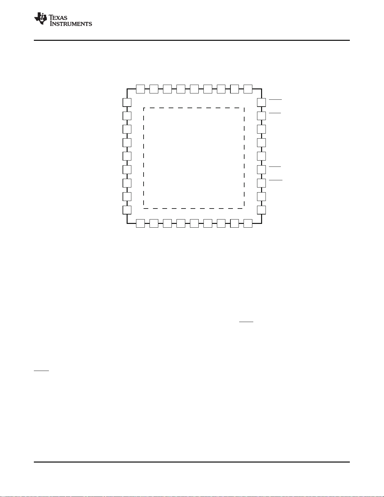
SUPPLY CURRENT vs TEMPERATURE SUPPLY CURRENT vs INPUT VOLTAGE
Figure 6. Figure 7.
CURRENT LIMIT THRESHOLD vs TEMPERATURE BLOCKING TURNOFF THRESHOLD vs TEMPERATURE
Figure 8. Figure 9.
Copyright © 2010, Texas Instruments Incorporated Submit Documentation Feedback 9
Product Folder Link(s): TPS2456
Page 10
9
9.5
10
10.5
11
11.5
12
-40 -20 0 20 40 60 80 100 120
T -JunctionTemperature-°C
J
(V -V )-mV
INx OUTx
GAT1x,
10V/div
OUTxstartingupinto500 (24mA)
Outputcapacitanceis830 FWm
675mV
MONx,
0.5V/div
OUTx,
10V/div
40mV
Time-1ms/div
OUTxstartingupinto1.8 (6.7 A,80W)
Outputcapacitanceis830 FWm
675mV
580mV
Time-1ms/div
GAT1x,
10V/div
MONx,
0.5V/div
OUTx,
10V/div
TPS2456
SLVSA78A –MARCH 2010–REVISED MARCH 2010
TYPICAL CHARACTERISTICS (continued)
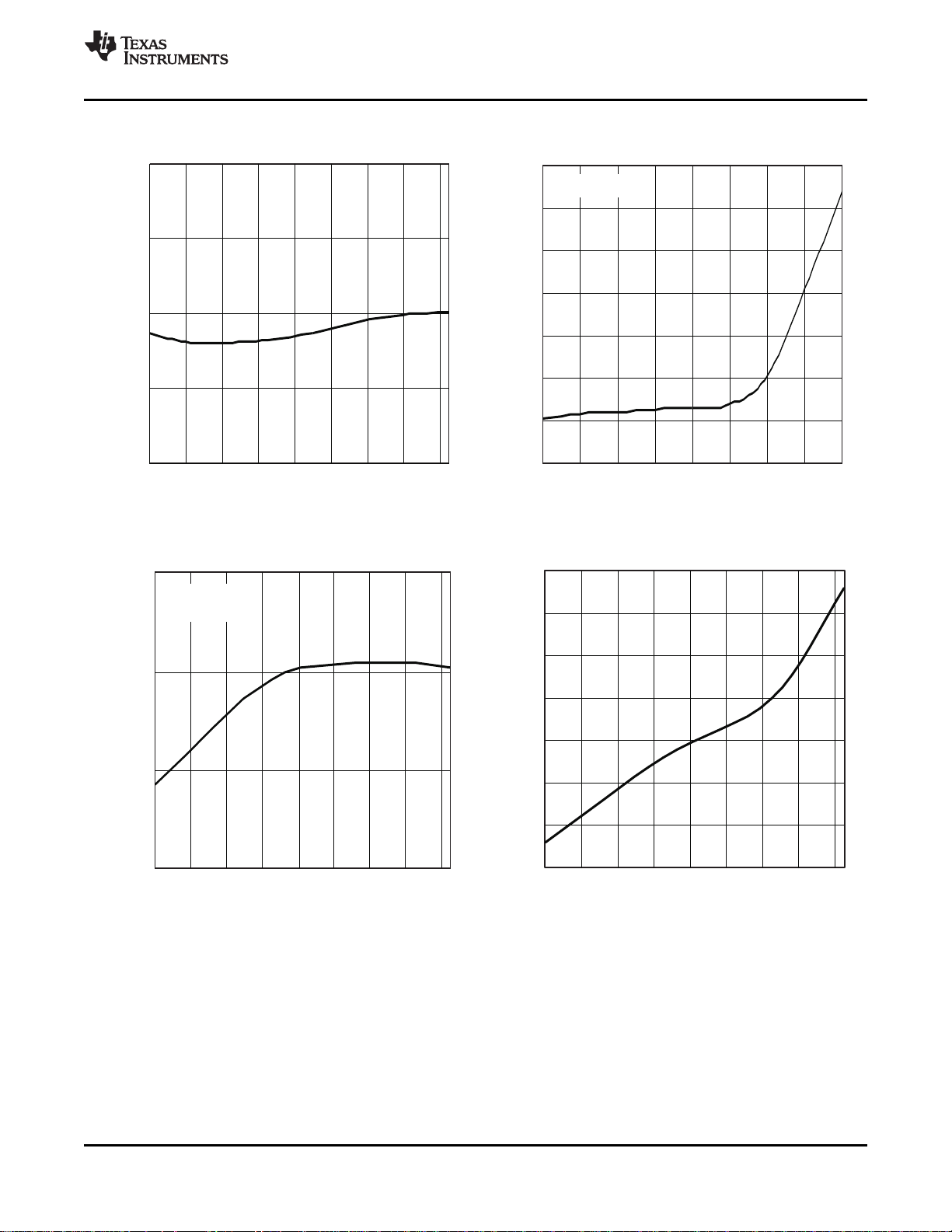
BLOCKING TURN ON THRESHOLD vs TEMPERATURE
www.ti.com
Figure 10.
Figure 11. Startup into 500 Ω, 830 µF Load Figure 12. Startup into 80 Watt, 830 µF Load
10 Submit Documentation Feedback Copyright © 2010, Texas Instruments Incorporated
Product Folder Link(s): TPS2456
Page 11

OUTxshortedwhiledriving6.7 A load
Outputcapacitanceis47 Fm
620mV
675mV
Time-2ms/div
GAT1x,
10V/div
MONx,
1V/div
OUTx,
10V/div
OUTxshortedwhiledriving6.7 A load
Outputcapacitanceis47 Fm
620mV
Time-1 s/divm
GAT1x,
10V/div
MONx,
1V/div
OUTx,
10V/div
GAT1x,
2V/div
OUTxstartingintoshortcircuit
675mV
MONx,
0.5V/div
OUTx,
20mV/div
2.9V
Time-1ms/div
GAT1x,
10V/div
OUTxoverloadedwhilesupplying6.7 A
970mV
MONx,
0.5V/div
OUTx,
10V/div
675mV
Time-1ms/div
TPS2456
www.ti.com
SLVSA78A –MARCH 2010–REVISED MARCH 2010
TYPICAL CHARACTERISTICS (continued)
Figure 13. Short Circuit Under Full Load (6.7 A) Wide Figure 14. Short Circuit Under Full Load (6.7 A) Zoom View
Figure 15. Startup into Short Circuit Figure 16. Overloaded while Supplying 6.7 A
SYSTEM OPERATION
INTRODUCTION
The TPS2456 controls two 12-V channels, or power paths. The channels can draw from a single common
supply, or from two independent supplies. The following sections describe the TPS2456 operation and provide
guidance for designing systems around this device.
CONTROL LOGIC AND POWER-ON RESET
The TPS2456 circuitry draws bias power from any of the INx or OUTx pins through an internal preregulator that
generates VINT. A bypass capacitor from VINT to ground provides decoupling and output filtering for the internal
circuits. Bias supply ORing allows the internal circuitry to function regardless of which channels receive power or
are in a faulted state. The four external MOSFET drive pins (GAT1A, GAT1B, GAT2A, and GAT2B) are held low
during startup to ensure that the channels remain off. When the voltage on the internal VINT rail exceeds
approximately 1 V, the power-on reset (POR) circuit initializes the TPS2456 and allows normal operation.
Copyright © 2010, Texas Instruments Incorporated Submit Documentation Feedback 11
Product Folder Link(s): TPS2456
Page 12

TPS2456
SLVSA78A –MARCH 2010–REVISED MARCH 2010
www.ti.com
ENABLE FUNCTIONS
The TPS2456 has two external enable pins for each of the channels.
The GAT1x and GAT2x pins are held low when the ENx pin is low. A high on ENx enables GAT1x for normal
control by the startup and protection features. Toggling ENx low, then high, clears a latch-off condition after a
fault has occurred on the channel.
The GAT2x pin is held low when the ORENx or ENx pins are low. The reverse blocking comparator-driven state
machine controls GAT2x when ORENx and ENx pins are high.
ENx ORENx PROTECTION BLOCKING
0 0 Disabled (low) Disabled (low)
0 1 Disabled (low) Disabled (low)
1 0 Enabled Disabled (low)
1 1 Enabled Enabled
(M1x, GAT1x) (M2x, GAT2x)
Each of the four enable pins has an internal 200 kΩ pullup resistor to VINT.
POWER GOOD (PGx) OUTPUTS
The TPS2456 provides an active-low open-drain Power Good (PGx) output for each channel. PGx goes low
(output good indication) for rising V
100 µs deglitch filter aids in avoiding false indications due to noise.
exceeding 10.63 V and PGx goes high for falling V
OUTx
below 10.5 V. A
OUTx
FAULT (FLTx) OUTPUTS
The TPS2456 provides an active-low open-drain fault output for each channel. The FLTx output pulls low when
the channel has remained in current limit long enough for the fault timer to expire (V
> 1.35 V). A channel
CTx
experiencing a fault timeout shuts down and latches off. Toggle the faulted channel’s ENx low and high to clear
the fault and re-enable the channel.
CURRENT LIMIT AND FAST TRIP THRESHOLDS
Load current is monitored by sensing the voltage across R
to 10 mΩ. Each channel features two distinct thresholds, a current-limit threshold and a fast-trip threshold.
The current limit threshold sets the regulation point of a feedback loop. If the current flowing through the channel
exceeds the current limit threshold, V
is reduced, forcing the MOSFET into linear operation. This causes the
GAT1x
current flowing through the channel to settle to the value determined by the current limit threshold. For example,
when a module first powers up, it draws an inrush current to charge its load capacitance. The current-limit loop
ensures that this inrush current does not exceed the current limit threshold. M1 will dissipate much more power
in current limit than during normal operation. The fault timer circuit limits the interval M1 operates in this
condition.
There is a delay before channel current is regulated following the onset of an overload during normal operation.
The current limit circuit is able to sink 30 µA from the protection MOSFET gate. The delay is the result of the
MOSFET’s C
discharge from (V
ISS
+ 13 V) to ( V
INx
INx
threshold voltage. Overloads between the current limit and the fast trip threshold will be permitted for this period.
This is demonstrated by Figure 16. Currents above the fast trip threshold are handled by rapidly turning the
protection MOSFET off with a strong gate pulldown that is driven by a 10 µs oneshot. The fault timer starts and
the gate is allowed to rise after the oneshot completes in what resembles a normal startup.
The fast trip threshold protects the MOSFET and channel components against a severe short that creates a high
current faster than the current-limit loop can control. If (V
SENPx
GAT1x and GAT2x are immediately pulled to GND for a minimum of 10µs. The channel turns back on slowly,
allowing the current limit feedback loop time to take over. The fault timer period limits the duration the MOSFET
will see this stress. This is demonstrated by Figure 13 and Figure 14.
, whose values typically lie in the range of 4 mΩ
SENSEx
+ V
T_M1x
– V
SENMx
) where V
is the protection MOSFET's
T_M1x
) exceeds the 100 mV fast trip threshold,
12 Submit Documentation Feedback Copyright © 2010, Texas Instruments Incorporated
Product Folder Link(s): TPS2456
Page 13

FTx
SEN SEx
100 mV
I =
R
SEN SEx SEN SEx
MON x MON x
SETx
R I
V = R
R
æ ö
´
´
ç ÷
è ø
SETx
LIMIT x
MON x S EN SEx
R
I = 0.675 V
R R
æ ö
´
ç ÷
´
è ø
LIMITx MONx SENSEx
SETx
I R R
R =
0.675 V
´ ´
TPS2456
www.ti.com
SLVSA78A –MARCH 2010–REVISED MARCH 2010
When the TPS2456 protects a supply output in configurations that allow the loads to hotplug, pay special
attention to coordinating load surges (due to input capacitance) and the fast trip threshold. The fast trip threshold
may need to be set 2–5 times higher than the current limit to accommodate this. Care must also be taken if the
INx voltages can have fast rising transients. The resulting charge current to capacitors on OUTx can potentially
exceed the fast trip threshold.
FAST TRIP AND CURRENT LIMITING
Figure 17 shows a simplified block diagram of the fast trip and current limit circuitry. Each channel requires an
external N-channel protection MOSFET and three external resistors. These resistors allow the user to
independently set the fast trip threshold and the current limit threshold, as described below.
The fast trip function is designed to protect the channel against short-circuit events. If the voltage across R
exceeds 100 mV, the TPS2456 immediately turns off the protection MOSFET, M1x. The nominal fast trip limit I
is defined in Equation 1.
The current limit circuit regulates V
to control the channel current from exceeding I
GAT1x
. The current limit
LIMITx
circuitry includes two amplifiers, A1and A2, as shown in Figure 17 and Figure 4. Amplifier A1forces the voltage
across external resistor R
through R
also flows through external resistor R
SETx
Amplifier A2implements a slow-reacting current limit. As long as V
normally. When V
exceeds 0.675 V, amplifier A2causes a small current to be drawn from GAT1x. The
MONx
to equal the voltage across external resistor R
SETx
, generating a voltage on the MONx pin per Equation 2.
MONx
MONx
. The current that flows
SENSEx
is less than 0.675 V, GAT1x operates
gate-to-source voltage of M1x drops until load current is reduced and the two inputs of amplifier A2balance. The
current flowing through the channel then equals I
per Equation 3.
LIMITx
SENSEx
FTx
(1)
(2)
The recommended value of R
is 6.81 kΩ. This resistor should be greater than 675 Ω to prevent excessive
MONx
currents from flowing through the internal circuitry.
(3)
(4)
Copyright © 2010, Texas Instruments Incorporated Submit Documentation Feedback 13
Product Folder Link(s): TPS2456
Page 14

R
MONx
+
SENMx
MONx
675mV
+
100mV
Fast Trip
Comparator
Current
Limit Amp
+
30mA
GAT1x
A1
A2
100
R
SENSEx
R
SETx
SENPx
SETx
60mA
V
CP
I
FT,LIMIT
GAT1x(sourcing)
GAT1x
Gate-M1x
I
dV
dt C
@
OUTx GAT1x
INx_INRUSH OUTx OUTx
dV dV
I = C = C
dt dt
´ ´
TPS2456
SLVSA78A –MARCH 2010–REVISED MARCH 2010
www.ti.com
Figure 17. Over-Current Protection Circuitry
TURN ON AND INRUSH SLEW RATE CONTROL
One of the main functions of a protection device is to provide a method of hot-plugging and starting up a unit in a
low-stress and controlled manner. Starting includes the ability to charge the output capacitance (on OUTx)
without overburdening the input power bus while minimizing the stress on the protection MOSFET. Two possible
charge-rate control methods are possible with the TPS2456, current limited and gate dv/dt controlled.
As normally configured, the gate dv/dt turn-on slew rate is described by Equation 5.
where I
GAT1x(sourcing)
transfer capacitance, C
= ΔQg/ VTwhere ΔQgis the width of the plateau region and VTis the gate plateau voltage. To simplify the
calculation, the MOSFET gate capacitances are assumed to be fixed, while in reality, there is a voltage
dependency. The output voltage tracks V
limit is not active. The inrush current is defined by the following equation for a purely capacitive load. Startup of a
switching converter load during inrush should be avoided by use of PGx to control the converter.
The actual inrush current is the lesser of the current limit (Equation 3) or dv/dt-limited inrush current.
To reduce the slew rate, increase C
resistor of at least 1000 Ω in series with the additional capacitance to prevent it from interfering with the fast turn
off of the MOSFET.
equals the current sourced by the GAT1x pin (nominally 30 µA) and C
. Average C
RSS
may be approximated using the MOSFET V
RSS
GATE_M1x
Gate-M1x
once it has exceeded the MOSFET threshold voltage if current
by connecting additional capacitance from GAT1x to ground. Place a
Gate-M1x
vs. Qggraph as C
GATE
is the reverse
(5)
RSS
(6)
14 Submit Documentation Feedback Copyright © 2010, Texas Instruments Incorporated
Product Folder Link(s): TPS2456
Page 15

fx Tx
-6fx
Tx f x
1.35 V
t = C
10 μA
OR
t 10 μA
C = = t 7.4 10
1.35 V
´
´
´ ´
( )
ISS_M1x T_M1x
ISS_M1x TM1x RSS_M1x IN1x
INRUSH
GAT1x GAT1x GAT1x
ISS_M1x
ISS_M1x TM1x
OUTx IN1x
INRUSH
GAT1x LIMITx
Gate dv/dt Limited Inrush
C 6 V V
C V C V
t = + +
I I I
Current Limited Inrush
C 6 V V
C V
C V
t = + +
I I
´ -
´ ´
´ -
´
´
( )
T_M1x
GAT1x
I
TPS2456
www.ti.com
SLVSA78A –MARCH 2010–REVISED MARCH 2010
FAULT TIMER PROGRAMMING
Each channel requires an external capacitor CTxconnected between the CTx pin and ground. The TPS2456
sources 10 µA into CTxwhen the gate voltage is low ((V
V
the channel off if current limit persists long enough for V
200 Ω pull-down resistor when (V
as an indication that current limit is active. The TPS2456 pulls GAT1x and GAT2x to ground and latches
GAT1x
CTx
GAT1x
– V
) > 6 V) and FLTx is not active. The nominal fault time tfxis defined
INx
by Equation 7.
Converter startup typically sets the minimum tfx. There are three important intervals to consider when calculating
the time to set tfx, initial charge of the MOSFET gate to the threshold voltage, the interval as V
and the interval for V
GAT1x
to exceed V
by 6 V. Assume that a constant C
INx
periods since the MOSFET drain and source voltages do not change. The middle period may be controlled by
either current limit or gate dv/dt limit as previously discussed. Let V
the inrush current.
– V
GAT1x
) < 6 V). The timer circuit interprets a low
INx
to reach 1.35 V. CTxis discharged through a nominal
rises to V
is charged in the first and third
ISS
be the MOSFET gate voltage to sustain
TM1x
OUTx
(7)
INx
,
Many of these parameters have wide tolerance, thus, the above approximation provides an initial estimate.
Provide sufficient margin in the CTxselection to assure the channel starts reliably while not becoming overly long.
Shorter fault times reduce the stresses imposed on the protection MOSFET under fault conditions, permitting the
use of smaller, less expensive protection MOSFETs.
ENx RESET PERIOD
The TPS2456 will latch off after a current limit that persists long enough to trip the fault timer. The TPS2456 may
be re-enabled by cycling the ENx false (low), then high. There is a minimum low period required to fully reset
C
that is determined by the R x C period where R is the internal discharge resistance. Calculate the minimum
CTx
period as t
ENx_LOW_MIN
nF x 1.2) x 400 x 3 = 31.7 µs. t
= C
CTx_MAX
ENx_LOW_MIN
x 400 Ω x 3. Assuming C
BLOCKING OPERATION
Each channel may use an external MOSFET (M2x) to provide reverse blocking. This feature is often used where
two inputs are ORed together to a common output for redundancy. Blocking protects the common output from
being drawn down if an input is shorted, and maintains the independence of both inputs. Blocking may not be
required in all system topologies. The TPS2456 pulls the GAT2x pin high when V
pulls the pin low when this differential falls below –3 mV (V
mV of hysteresis to help prevent false triggering as shown in Figure 18. This technique will allow some reverse
current to flow, but provides positive detection in the event of a real fault.
The blocking MOSFET is oriented so its body diode conducts forward current and blocks reverse current. The
body diode does not normally conduct current because the MOSFET turns on when the voltage differential
across it exceeds 10 mV.
Copyright © 2010, Texas Instruments Incorporated Submit Documentation Feedback 15
CTx_MAX
is 22 nF at 20% tolerance, t
should always be greater than 100 ns.
is greater than V
OUTx
Product Folder Link(s): TPS2456
ENx_LOW_MIN
(INx–OUTx)
). These thresholds provide 13
INx
exceeds 10 mV, and it
(8)
= (22
Page 16

V
INx
+ 13V
GND
10mV
- 3mV
V
GAT2x
(V
INx-VOUTx
)
TPS2456
SLVSA78A –MARCH 2010–REVISED MARCH 2010
www.ti.com
Figure 18. Blocking Thresholds
APPLICATION INFORMATION
SYSTEM DESIGN CONSIDERATIONS
The TPS2456 has two independent 12 V sections which provide protection and blocking (ORing). These sections
may be used in multiple configurations.
• TPS2456 on the power input of a system
– Two redundant input power rails to a single output (see Figure 1)
– Blocking protects output when one of the inputs is shorted
– Two independent loads powered by two separate or one common input rail
– Blocking not required
– Two redundant input rails ORed (no protection) to one common output
• TPS2456 on the power output of a system
– Up to two output rails with protection
– Protection isolates faulted output bus
– Enable can be used to turn output on and off
– Up to two output power rails with protection and blocking
– Used where multiple outputs are tied together
The system power architecture drives the topology that best suits a particular design.
DESIGN EXAMPLE: CURRENT LIMITED START-UP
The following example is for a single channel protection circuit using current-limited inrush control. The design of
the second channel would follow the same procedure and is not shown since it is redundant.
For this design example, a system board with 1000 µF of capacitance and a dc load of 1.6 Ω (or 7.5 A) must be
able to be hot plugged into a 12 V main bus supply. The main bus supply has a peak fault current capability of
20 A. Operating above 20 A of current draw runs the risk of opening a circuit breaker and shutting the system
down. The average current budgeted for the system board is 7.5 A under normal conditions. The main bus can
supply up to 10.1 A peak for up to 10 ms during start-up or transient conditions. This procedure assumes that the
inrush current is not limited by the gate charge rate. The basic system block diagram is shown in Figure 19.
16 Submit Documentation Feedback Copyright © 2010, Texas Instruments Incorporated
Product Folder Link(s): TPS2456
Page 17

12V Main Bus Supply
Specifications (per output):
Peak Fault Current = 20A
Peak Current Limit = 10.1A
Average Current = 7.5A
M1x
R
SENSEx
0.1mF
0.1mF
C
LOADx
1000mF
R
LOADx
1.6W
R
MONx
R
SETx
R
GATEx
SENMx
SETx
SENSPx
INx
MONx
GND
GATE1x
OUTx
Part of TPS2456
LOADPROTECTION
Multiple Outputs
Possible
C
Tx
CTx
SENSEx
FTx
100mV 100mV
R = = = 5mΩ
I 20A
W
2 2
RSENSEx LIMITx SENSEx
P = I × R = 10.1 × 5m = 0.51Watts
W W
W
LIMITx MONx SENSEx
SETx
I ×R ×R
10.1A × 6.81k ×0.005
R = = = 509
0.675V 0.675V
TPS2456
www.ti.com
SLVSA78A –MARCH 2010–REVISED MARCH 2010
Figure 19. 12 V Main Bus
Select R
The first step is to calculate R
SENSEx
SENSEx
which sets the fast current trip point, I
. This is the maximum current that
FTx
can pass through M1x and is meant to protect against short circuits. Calculate R
peak fault current (I
) of 20 A.
FTx
SENSEx
using Equation 9 for a
The R
SENSEx
resistor is in series with the main power path and should have a power rating sufficient to support
the full load current. The 12 V main bus has budgeted 10.1 A for this board, so this is the value of limit used for
further calculations including the power dissipated in R
Equation 10. A higher wattage rating should be used based on local derating practice (for example 50%).
Select R
Next, R
calculation of R
I
LIMITx
Choose R
SETx
is calculated to set the channel current limit (I
SETx
SETx
to calculate R
as the closest standard value, 511 Ω.
SETx
. Use the recommended 6.81kΩ for R
.
SETx
Estimate Output Charge Time
The system can provide 10.1 A of peak current for 10 ms. This current can be used for start-up of the system
board as long as the output capacitance can be charged up to 12 V in less than 10 ms while also supplying
current to the load resistance connected in parallel to the output capacitor. The charge time is estimated using
Equation 12. For this equation, V
OUTx
is the final nominal voltage for the board (12 V), R
board (1.6 Ω), and there is a small amount of time for the pass transistor’s gate capacitance to charge to the
threshold voltage. This time, typically around 100 µs, is added to the end of the equation to provide a better
estimate of the total start-up time.
Copyright © 2010, Texas Instruments Incorporated Submit Documentation Feedback 17
Product Folder Link(s): TPS2456
SENSEx
MONx
. The power dissipated by R
) to 10.1 A. R
LIMITx
MONx
is also a variable in the
is calculated using
SENSE
(although other values can be used) and 10.1 A for
is the dc load of the
LOAD
(9)
(10)
(11)
Page 18

m
æ ö
÷
ç
÷
»
ç
÷
ç
÷
ç
è ø
LIMITx LOADx OUTx
CHG LOADx LOADx
LIMITx LOADx
I ×R - V
t -R × C × ln +100 s
I ×R
m m
æ ö
W
÷
ç
» W
÷
ç
÷
ç
è ø
W
CHG
10.1A ×1.6 -12V
t -1.6 ×1000 F×ln +100 s
10.1A ×1.6
»
CHG
t 2.27ms
m
LOADx OUTx
CHG
LIMIT_M1x
C × V
t = +100 s
I
2
Dx DS(on)_M1x LIMITx
P = R ×I
TPS2456
SLVSA78A –MARCH 2010–REVISED MARCH 2010
www.ti.com
(12)
(13)
(14)
The estimated time to charge the output is 2.27 ms. It is safe to allow the board to power up using the peak
current limit because t
is below the 10ms target.
CHG
Equation 12 assumes there is a resistive load on the output during the ramp up so the output voltage has an
“RC” shape. The output capacitance charges linearly if the load is purely capacitive, simplifying the charge time
equation to the following.
(15)
Select M1x
The next design step is to select M1x. The TPS2456 is designed to use N channel MOSFETs as protection
devices. The maximum MOSFET gate to source voltage rating, V
, must be high enough to support the
GS-MAX
highest of the gate drive (14.5 V) or input voltage.
The next factor to consider is the drain to source voltage rating, V
, of the MOSFET. From a dc perspective,
DS-MAX
the MOSFET needs to withstand the input power supply voltage of 12 V for this example. However; the MOSFET
can be exposed to high voltage spikes during fault conditions. For this reason, a MOSFET with a substantially
higher V
DS-MAX
(snubber, TVS, diodes, etc.). Look for a V
rating improves the system reliability and provides voltage headroom for transient protection
DS-MAX
rating with a minimum of twice of the input power supply voltage.
Next, the dc power loss of the MOSFET must be considered. The power dissipation of the MOSFET is directly
related to the R
of the MOSFET. The dc power dissipation for the MOSFET can be calculated using
DS(on)
Equation 16.
(16)
Taking these factors into consideration, the TI CSD16403Q5A was selected for this example. The
CSD16403Q5A has a V
GS-MAX
rating of 16 V, V
rating of 25 V, an R
DS-MAX
of 2.2 mΩ, and an R
DS(on)
qJA-MAX
of 51
°C/W.
During normal circuit operation, the MOSFET can have up to 10.1 A flowing through, which equates to 0.22 W
(I2xR) and an 11°C rise in junction temperature (P x R
). This is well within the data sheets limits for the
qJA-MAX
MOSFET. The power dissipated during a fault (e.g. output short) is substantially larger than the steady-state
power. The power handling capability of the MOSFET needs to be checked during fault conditions.
Most MOSFET data sheets provide a Safe Operating Area (SOA) plot. This plot can be used to check if the
MOSFET can survive the power form a transient fault condition. Figure 20 shows the SOA curve for the
QSD16403Q5A. The maximum fault current is set to 20 A for the 12 V input bus. This point can be located on
Figure 20. The diagonal lines tell the length of time this transient can be safely applied to the QSD16403Q5A.
The transistor can survive a 12 V, 20 A transient for approximately 9 ms.
18 Submit Documentation Feedback Copyright © 2010, Texas Instruments Incorporated
Product Folder Link(s): TPS2456
Page 19

1k
10
0.01
1
100
I
D
− DrainCurrent − A
0.1
0.01 0.1 10
12
1001
SinglePulse
R
qJA
=94 C/W(minCu)
o
1ms
10ms
100ms
1s
DC
AreaLimited
byR
DS(on)
VDS− Drain ToSourceVoltage − V
æ ö
÷
ç
÷
ç
÷
ç
÷
ç
è ø
T_M1x ISS_M1x
LIMITx LOADx OUTx
CHG LOADx LOADx
LIMITx LOADx G
V ×C
I ×R - V
t = -R × C × ln +
I ×R I
æ ö
÷
ç
÷
ç
÷
ç
÷
ç
è ø
TM1x ISS_M1x
LIMITx LOADx OUTx
TMR_MIN LOADx LOADx
LIMITx LOAD G
(6 V + V ) × C
I ×R - V
t = -R × C × ln +
I ×R I
TPS2456
www.ti.com
SLVSA78A –MARCH 2010–REVISED MARCH 2010
Figure 20. Drain To Source Voltage
The turn off time of the TPS2456 and MOSFET should be taken into account. The TPS2456 detects the fault
condition as soon as the current through the sense resistor reaches 20 A. There is a 300 ns maximum
propagation delay for the TPS2456 to start discharging the MOSFET gate. The MOSFET has an additional
turn-off delay due to gate discharge (see Sinking current - Fast Discharge). The total delay for the TPS2456 and
the CSD16403Q5A is approximately 310 ns. The fault current continues to rise above 20 A for this period. The
rise of the fault current is determined by any inductance and resistance in the power path as well as the
impedance of the input voltage source. Continuing to follow the 12 V line up on the SOA curve, it can be seen
that the CSD16403Q5A could handle peak currents up to 180 A for 1 ms, giving substantial margin in this
design. This makes this transistor a good choice for this application.
Output Charge Time Refinement
A more accurate charge time can be calculated using Equation 17, now that the MOSFET has been chosen. This
is the same as Equation 15, but the 100 µs term is replaced with the variables that determine the time it takes to
charge the gate of the MOSFET up to the threshold voltage. The threshold voltage used in this equation should
be the voltage where the Mosfet starts to conduct higher currents. This can be found in the MOSFET data sheet
from graphs showing IDvs. VGS. For the CSD16403Q5A, the V
is 1.6 V, and C
T_M1x
is 2040 pF. The term IGin
ISS
Equation 17 is the GAT1x sourcing current, typically 30 µA. Using these values, Equation 17 gives a charge time
of 2.28 ms
(17)
Select C
Tx
The next step is to determine the minimum fault timer period. In the previous section, the change time calculation
yielded 2.28 ms. This is the amount of time it takes to charge the output capacitor up to the final output voltage.
However, the fault timer uses the difference between the input voltage and the gate voltage to determine if the
TPS2456 is in current limit. The fault timer continues to run until V
GATE_M1x
is 6 V above the input voltage. Some
additional time must be added to the charge time to account for this additional gate voltage rise. The minimum
fault timer time can be calculated using Equation 18.
(18)
Copyright © 2010, Texas Instruments Incorporated Submit Documentation Feedback 19
Product Folder Link(s): TPS2456
Page 20

m
m
FAULT
Tx
t × 10 A
0.008s ×10 A
C = = = 59nF
1.35V 1.35V
M1x
To
Load
GND
GATE1x
Part of
TPS2456
C
ADD
1kW
I
G
30mA
From
Source
GATE_M1x
OUTx G
RSS_M1x ADD
dV
dV I
= =
dt dt C +C
OUTx OUTx G
INx_PEAK
LOADx RSS ADD
V C ×I
I = +
R (C + C )
TPS2456
SLVSA78A –MARCH 2010–REVISED MARCH 2010
www.ti.com
Using the example numbers in the above equation leads to a minimum fault timer time of 2.688 ms. The fault
timer must be set to a value higher than 2.688 ms to avoid turning off during start-up but lower than any
maximum time limit. There is a maximum time limit set by the SOA curve of the MOSFET. Referring back to
Figure 20, the CSD16403Q5A SOA curve, the MOSFET can tolerate 10.1 A with 12 V across it for approximately
20 ms. However; the input power supply can only supply the 10.1 A for 10 ms. Therefore, the fault timer should
be set to between 2.688 ms and 10 ms. For this example, select 8 ms to allow for variation of system parameters
such as temperature, load, component tolerance, and input voltage. The timing capacitor is calculated in
Equation 19 as 59 nF. Select a the next highest standard value, 62 nF, yielding an 8.37 ms fault time.
(19)
Blocking Device, M2x
Since this example uses a single channel, there is no need for the blocking MOSFET, and it can be left out of the
circuit. No connection needs to be made to the GAT2x or ORENx pins.
DESIGN EXAMPLE: GATE RAMP LIMITED STARTUP
In the first example, the output capacitance is charged in current limit. In some applications, the current limit is
the absolute maximum that the circuit should see, so charging the output up in current limit is not an option. In
this case, it is necessary to slow down the output voltage ramp so that the current limit is not reached. This can
be done by adding additional capacitance to M1x's gate.
The gate of the pass transistor is driven by a 30 µA (typical) current source. The current charges the gate to
source and gate to drain (C
lengthened by adding a capacitor, C
series with the additional capacitance as shown in Figure 21.
) capacitance, producing a voltage ramp at the gate. The time of the ramp can be
rss
, between the gate and ground. A 1 kΩ resistor should be placed in
ADD
With C
, the output voltage ramp is equal to:
ADD
The peak current, I
INX-PEAK
, that is reached with the new ramp rate is:
20 Submit Documentation Feedback Copyright © 2010, Texas Instruments Incorporated
Figure 21.
(20)
(21)
Product Folder Link(s): TPS2456
Page 21

( )
( ) ( )
T_M1x ISS ADD
OUTx RSS ADD ISS ADD
TMR_MIN
G G G
V C + C
V × C + C 6× C + C
t = + +
I I I
LOAD
INTER-
CONNECT
INTER-
CONNECT
POWERSUPPLY
TPS2456
GAT1x GAT2x
OUTx
INx
SENMx
SENPx
1kW
100 100
C
GS
C
GD
BlockingMOSFET
C
DS
C
GS
C
GD
ProtectionMOSFET
C
DS
ESD
Diode
ESD
Diode
ESD
Diode
ESD
Diode
L
P
R
LOAD
E=LI2/2
OUTPUT
R
P
L
P
E=LI2/2
R
P
LP+
L
EMI_FILTER
L
P
L
P
E=LI2/2
R
P
L
P
E=LI2/2
R
P
+
INPUT
C
IN
C
OUT
TPS2456
www.ti.com
C
can be adjusted so that I
ADD
INx_PEAK
is less than I
avoiding current limit start-up. Using a controlled gate
LIMITx
SLVSA78A –MARCH 2010–REVISED MARCH 2010
ramp requires lower peak current, but takes longer to charge the output capacitance. The length of the fault time
needs to be selected to accomodate this longer ramp up time. The minimum time the fault timer should be set to
is described by Equation 22.
(22)
BYPASS CAPACITORS
It is a good practice to provide low-impedance ceramic capacitor bypassing of INx and OUTx. Values in the
range of 10 nF to 1 µF are recommended. Some system topologies are insensitive to the values of these
capacitors; however, some are not and prefer to minimize the value of the bypass capacitor.
Input capacitance on a plug-in board may cause a large inrush current as the capacitor charges through the low
impedance power bus when inserted. This stresses the connector contacts and causes a short voltage sag on
the input bus. Small amounts of capacitance (e.g., 10 nF to 0.1 µF) are often tolerable in these systems.
Filter capacitors at the output of a redundant plug-in board are useful for controlling voltage transients, but they
may can cause problems when the board is inserted into an active bus. If the output capacitor charge from an
active bus is not limited, the inrush surge might engage the active supply's fast-trip shutdown. One possible
solution is to put a few Ohms of resistance in series with the capacitor to limit inrush below the fast trip level.
TRANSIENT PROTECTION
If the TPS2456 is used in applications which have large input and output capacitors, voltage transients during
load steps or short circuits are controlled and pose no problems.
TPS2456 devices are sometimes deployed systems that may have long, inductive feed or load interconnections.
The effect of the inductance, with little local capacitance, gives rise to potential voltage transient issues. A
simplified model of this is shown in Figure 22. Channel current transients may be caused by events such as
hot-plug, output shorts with fast turnoff, or abrupt load changes. The combination of input inductance and an
abrupt load decrease causes a positive voltage spike on the TPS2354 INPUT pins. The combination of output
inductance and an abrupt load decrease will cause a negative voltage spike on the TPS2354 OUTPUT. These
transients have the potential to exceed the Absolute Maximum Ratings, either damaging the TPS23754 or
causing undesired operation.
NOTE: LP= Parasitic Inductance (not all instances equal)
RP= Parasitic Resistance (not all instances equal)
Copyright © 2010, Texas Instruments Incorporated Submit Documentation Feedback 21
Figure 22. System Transient Model
Product Folder Link(s): TPS2456
Page 22

SPIK E INIT L OAD
L
V = V + I
C
( )
2
LOA D
2
SPI KE N OM
L I
C =
V V´-
CL_M AX BR_MIN
SER IES
PEAK _PULS E T EST
V V
21.5 V 14.4 V
R = = = 0.102
I I 69.7 A 1 mA
-
W
- -
ABS_MAX BR_MAX
CL_MAX
SERIES
V V
17 V 15.9 V
I = = = 10.8 A
R 0.102
-
-
TPS2456
SLVSA78A –MARCH 2010–REVISED MARCH 2010
www.ti.com
An analysis must be performed to determine the need for transient protection. Equation 23 allows the designer to
estimate the voltage spike due to current interruptions.
(23)
Where:
V
= initial voltage at terminal being analyzed before the current is interrupted
INIT
L = combined inductance of feed and RTN lines in series with interrupted current
C = capacitance at point of computation
I
= current immediately before circuit is opened
LOAD
An approximation for the inductance of a straight wire is:
L ≈ [0.2 × length_in_meters × (In(4 × length/diameter) – 0.75)] nH
The capacitance in Equation 23, at INPUT, consists of parasitic capacitance and any intentional bypass
capacitance. This implies that the transients can be controlled by the addition of sufficient capacitance.
Equation 24 can be used to calculate the capacitance required to limit the voltage spike to a desired level above
the nominal voltage.
(24)
TRANSIENT PROTECTION SOLUTIONS
Typical protection solutions involve capacitors, TVSs ( Transient Voltage Suppressors ) and/or a Schottky diode.
A TVS and small bypass capacitor at INPUT (see Figure 22) are the most likely solutions to solve input voltage
overshoot. The TVS must be selected so that its clamping is below the Absolute Maximum Rating (17 V) at the
anticipated fault current. For example, the SMCJ13A data sheet specifies a maximum clamping voltage of 21.5 V
(which exceeds the Absolute Maximum voltage) at 69.7 A. The actual clamping voltage at the fault current (IFT)
may be within the Absolute Maximum; however, the clamp voltage at lower currents must be estimated to verify.
By modeling the TVS as a perfect voltage clamp in series with a resistor, the clamping voltage may be estimated
at different currents per Equation 25.
The maximum permitted clamping current for this device is found in Equation 26. This is a worst case (low)
number.
A Schottky diode and capacitor across the OUTPUT (Figure 22) are the most likely solutions to clamp the
transient energy and limit the negative voltage excursion. Although the Schottky diode absorbs most of the
energy, the extremely fast di/dt at shutoff allows some of the leading edge energy to couple through the parasitic
capacitances of the protection and blocking MOSFET (CDS, CGS, CGD) to the GAT1x and GAT2x pins. Protection
for these pins is provided by 100 Ω resistors which have little effect on normal operation but provide good
isolation during transient events.
Equation 24 gives insight into selection of transient protection capacitors for both INPUT and OUTPUT; however,
there are concerns with adding a lot of capacitance in some situations. See the BYPASS CAPACITORS section
regarding considerations and limitations
PCB layout of the protection is critical to its performance. The layout should minimize the impedance between
the TPS2456 and the protection in order to provide the best clamping.
22 Submit Documentation Feedback Copyright © 2010, Texas Instruments Incorporated
Product Folder Link(s): TPS2456
(25)
(26)
Page 23

BLEED
BLEED
BLEED
V
R = 280 k
(6 V V )
´ W
-
MONB
MONA
Partof
TPS2456
R =R
R =R
SENSEA SENSEB
SETA SETB
R
MON
TPS2456
www.ti.com
SLVSA78A –MARCH 2010–REVISED MARCH 2010
OUTPUT BLEED RESISTANCE
The OUTx pin sources a small amount of current when the channel input is powered, but disabled in
non-redundant configurations (output is unpowered). The leakage can be modeled as a 6 V source in series with
a 280 kΩ resistor, allowing approximately 21.4 µA into a short. This leakage can charge a high-impedance load
to approximately 6 V. If this is unacceptable, control the output voltage in this state by adding a load resistor from
OUTx to GND. Select the resistor, R
, per Equation 27, where V
BLEED
is the desired maximum output
BLEED
voltage. Since the model is nominal, use a 25% smaller resistor value.
(27)
CONTROLLING FAULT CURRENT in REDUNDANT POWER TOPOLOGIES
System topologies such as Figure 1 are often used to provide power source redundancy. This permits the load to
run from either source, or potentially both in parallel. Blocking permits the load to operate uninterrupted in the
event of either source failing open or shorting to GND. However, this topology permits the load to draw twice the
channel fault current (I
The simple configuration of Figure 23 programs the total load fault current to a fixed value independent of the
number of channel feeds to the load. The current limit thresholds now apply to the sum of the currents delivered
by the redundant channels. When implementing this redundant mode, it is recommended that all of the channels
use the same R
SENSEx
between sources, it simply permits the power to flow from the higher source, but limits the maximum load current
to a fixed value.
) for two closely matched sources.
LIMITx
and R
values. This configuration does not foster sharing or smooth transitions
SETx
CURRENT FEEDBACK TO A SHELF CONTROLLER
A shelf controller can monitor channel currents by observing V
R
with an Analog to Digital Converter (ADC) to provide a digital representation of the current. Figure 24 shows a
typical system configuration using a multiplexer and ADC (analog to digital converter) to monitor the current in
both channels of the TPS2456. It has been assumed that the normal 0 V to 0.675 V range of V
the ADC input. If this is not the case, operational amplifier circuits should be used to buffer and scale these
signals. It is not advisable to add capacitance to the MONx pins as this effects the current-limit loop.
Copyright © 2010, Texas Instruments Incorporated Submit Documentation Feedback 23
. The voltage on MONx can be directly sampled with an analog circuit (e.g. a comparator) or sampled
SENSEx
Figure 23. Fixed Fault Current Application
, which is proportional to the current through
MONx
Product Folder Link(s): TPS2456
is suitable for
MONx
Page 24

ADC
MONa
MONb
6810
6810
TPS2456
2:1 Mux
μP
a0
a1
s0
LOADCURRENT
PATH
LOADCURRENT
PATH
Method 1
Method 2
R
SENSEx
R
SET
TPS2456
SENP
R
SET
SENM
SET
TPS2456
SENP
SENM
SET
TPS2456
SLVSA78A –MARCH 2010–REVISED MARCH 2010
www.ti.com
Figure 24.
The output of the MONx pin is a current proportional to the current passing through the pass transistor as defined
in Equation 2. The current flowing out of the MONx pin is converted to a voltage by R
kΩ. Any circuitry connected to the MONx pin should either have an input impedance much higher that R
which is typically 6.81
MONx
MONx
to
reduce measurement and limiting error, or the value of the parallel combination must be adjusted. The output of
the MONx pin can also be buffered using a unity gain, non-inverting operational amplifier if necessary.
LAYOUT CONSIDERATIONS
TPS2456 applications require layout attention to ensure proper performance and minimize susceptibility to
transients and noise. In general, all runs should be as short as possible, but the following list deserves first
consideration.
1. Decoupling capacitors on INA and INB should have minimal length to the pin and to GND
2. SENMx and SENPx runs must be short and run side-by-side to maximize common mode rejection. Kelvin
connections should be used at the points of contact with R
. (See Figure 25)
SENSEx
Figure 25. Recommended R
3. SETx runs need to be short on both sides of R
4. Power path connections should be as short as possible and sized to carry at least twice the full load current,
more if possible.
5. Connections to GND and MONx pins should be minimized after the connections above have been placed.
6. The device dissipates low power so soldering the powerpad to the board is not a requirement. However,
doing so improves thermal performance and reduces susceptibility to noise.
24 Submit Documentation Feedback Copyright © 2010, Texas Instruments Incorporated
SENSE
.
SETx
Product Folder Link(s): TPS2456
Layout
Page 25

TPS2456
www.ti.com
SLVSA78A –MARCH 2010–REVISED MARCH 2010
7. The board should use a single point ground scheme. The current return path for both channels should be
isolated from each other as much as possible and tie together at a single point. This helps to reduce ground
bounce and false turn offs in one channel when there is a fault in the other channel. Also, sensitive analog
grounds (such as the ground connections of R
x and CTx) should be run separate from the power path
MON
grounds. This analog ground must also tie to the two power path grounds at a single point. Figure 26 shows
the top layer routing of the TPS2456 EVM which uses a single point ground scheme. Each major power path,
the analog ground, and the single point tying them together is highlighted in the figure.
Figure 26.
8. Protection devices such as snubbers, TVS, capacitors or diodes should be placed physically close to the
device they are intended to protect, and routed with short trances to reduce inductance. For example, the
protection Schottky diode shown in Figure 1 should be physically close to the source of the pass transistor
(or the drain of the blocking MOSFET if used).
Copyright © 2010, Texas Instruments Incorporated Submit Documentation Feedback 25
Product Folder Link(s): TPS2456
Page 26

TPS2456
SLVSA78A –MARCH 2010–REVISED MARCH 2010
www.ti.com
REVISION HISTORY
Changes from Original (March 2010) to Revision A Page
• Changed data sheet status from Preview to Production ...................................................................................................... 1
• Changed the second paragraph of the DESCRIPTION From: The ORing control uses an external MOSFET to
prevent reverse current flow To: The ORing control uses an external MOSFET to block reverse current when an
input is shorted. .................................................................................................................................................................... 1
• Deleted the Dissipation Rating table and added the Thermal Information table .................................................................. 2
• Added test to the SENPA pin of the PIN FUNCTIONS table - Connect to the source side of R
• Changed PIN 32 From: GNDA To: GND and PIN 23 From: AGND To: GND in the DEVICE PINOUT illustration ............. 7
• Changed the DETAILED PIN DESCRIPTIONS .................................................................................................................... 7
• Changed Figure 8 Title From: FAST CURRENT LIMIT THRESHOLD vs TEMPERATURE To: CURRENT LIMIT
THRESHOLD vs TEMPERATURE, and added R
SETx
and R
values ............................................................................. 9
MONx
. .............................. 6
SENSEA
26 Submit Documentation Feedback Copyright © 2010, Texas Instruments Incorporated
Product Folder Link(s): TPS2456
Page 27

PACKAGE OPTION ADDENDUM
www.ti.com 19-Apr-2010
PACKAGING INFORMATION
Orderable Device Status
(1)
Package
Type
Package
Drawing
Pins Package
Qty
Eco Plan
TPS2456RHHR ACTIVE VQFN RHH 36 2500 Green (RoHS &
(2)
Lead/Ball Finish MSL Peak Temp
CU NIPDAU Level-3-260C-168 HR
(3)
no Sb/Br)
TPS2456RHHT ACTIVE VQFN RHH 36 250 Green (RoHS &
CU NIPDAU Level-3-260C-168 HR
no Sb/Br)
(1)
The marketing status values are defined as follows:
ACTIVE: Product device recommended for new designs.
LIFEBUY: TI has announced that the device will be discontinued, and a lifetime-buy period is in effect.
NRND: Not recommended for new designs. Device is in production to support existing customers, but TI does not recommend using this part in
a new design.
PREVIEW: Device has been announced but is not in production. Samples may or may not be available.
OBSOLETE: TI has discontinued the production of the device.
(2)
Eco Plan - The planned eco-friendly classification: Pb-Free (RoHS), Pb-Free (RoHS Exempt), or Green (RoHS & no Sb/Br) - please check
http://www.ti.com/productcontent for the latest availability information and additional product content details.
TBD: The Pb-Free/Green conversion plan has not been defined.
Pb-Free (RoHS): TI's terms "Lead-Free" or "Pb-Free" mean semiconductor products that are compatible with the current RoHS requirements
for all 6 substances, including the requirement that lead not exceed 0.1% by weight in homogeneous materials. Where designed to be soldered
at high temperatures, TI Pb-Free products are suitable for use in specified lead-free processes.
Pb-Free (RoHS Exempt): This component has a RoHS exemption for either 1) lead-based flip-chip solder bumps used between the die and
package, or 2) lead-based die adhesive used between the die and leadframe. The component is otherwise considered Pb-Free (RoHS
compatible) as defined above.
Green (RoHS & no Sb/Br): TI defines "Green" to mean Pb-Free (RoHS compatible), and free of Bromine (Br) and Antimony (Sb) based flame
retardants (Br or Sb do not exceed 0.1% by weight in homogeneous material)
(3)
MSL, Peak Temp. -- The Moisture Sensitivity Level rating according to the JEDEC industry standard classifications, and peak solder
temperature.
Important Information and Disclaimer:The information provided on this page represents TI's knowledge and belief as of the date that it is
provided. TI bases its knowledge and belief on information provided by third parties, and makes no representation or warranty as to the
accuracy of such information. Efforts are underway to better integrate information from third parties. TI has taken and continues to take
reasonable steps to provide representative and accurate information but may not have conducted destructive testing or chemical analysis on
incoming materials and chemicals. TI and TI suppliers consider certain information to be proprietary, and thus CAS numbers and other limited
information may not be available for release.
In no event shall TI's liability arising out of such information exceed the total purchase price of the TI part(s) at issue in this document sold by TI
to Customer on an annual basis.
Addendum-Page 1
Page 28

PACKAGE MATERIALS INFORMATION
www.ti.com 20-Jul-2010
TAPE AND REEL INFORMATION
*All dimensions are nominal
Device Package
Type
TPS2456RHHR VQFN RHH 36 2500 330.0 16.4 6.3 6.3 1.5 12.0 16.0 Q2
TPS2456RHHT VQFN RHH 36 250 180.0 16.4 6.3 6.3 1.5 12.0 16.0 Q2
Package
Drawing
Pins SPQ Reel
Diameter
(mm)
Reel
Width
W1 (mm)
A0
(mm)B0(mm)K0(mm)P1(mm)W(mm)
Pin1
Quadrant
Pack Materials-Page 1
Page 29

PACKAGE MATERIALS INFORMATION
www.ti.com 20-Jul-2010
*All dimensions are nominal
Device Package Type Package Drawing Pins SPQ Length (mm) Width (mm) Height (mm)
TPS2456RHHR VQFN RHH 36 2500 346.0 346.0 33.0
TPS2456RHHT VQFN RHH 36 250 190.5 212.7 31.8
Pack Materials-Page 2
Page 30

Page 31

Page 32

Page 33

IMPORTANT NOTICE
Texas Instruments Incorporated and its subsidiaries (TI) reserve the right to make corrections, modifications, enhancements, improvements,
and other changes to its products and services at any time and to discontinue any product or service without notice. Customers should
obtain the latest relevant information before placing orders and should verify that such information is current and complete. All products are
sold subject to TI’s terms and conditions of sale supplied at the time of order acknowledgment.
TI warrants performance of its hardware products to the specifications applicable at the time of sale in accordance with TI’s standard
warranty. Testing and other quality control techniques are used to the extent TI deems necessary to support this warranty. Except where
mandated by government requirements, testing of all parameters of each product is not necessarily performed.
TI assumes no liability for applications assistance or customer product design. Customers are responsible for their products and
applications using TI components. To minimize the risks associated with customer products and applications, customers should provide
adequate design and operating safeguards.
TI does not warrant or represent that any license, either express or implied, is granted under any TI patent right, copyright, mask work right,
or other TI intellectual property right relating to any combination, machine, or process in which TI products or services are used. Information
published by TI regarding third-party products or services does not constitute a license from TI to use such products or services or a
warranty or endorsement thereof. Use of such information may require a license from a third party under the patents or other intellectual
property of the third party, or a license from TI under the patents or other intellectual property of TI.
Reproduction of TI information in TI data books or data sheets is permissible only if reproduction is without alteration and is accompanied
by all associated warranties, conditions, limitations, and notices. Reproduction of this information with alteration is an unfair and deceptive
business practice. TI is not responsible or liable for such altered documentation. Information of third parties may be subject to additional
restrictions.
Resale of TI products or services with statements different from or beyond the parameters stated by TI for that product or service voids all
express and any implied warranties for the associated TI product or service and is an unfair and deceptive business practice. TI is not
responsible or liable for any such statements.
TI products are not authorized for use in safety-critical applications (such as life support) where a failure of the TI product would reasonably
be expected to cause severe personal injury or death, unless officers of the parties have executed an agreement specifically governing
such use. Buyers represent that they have all necessary expertise in the safety and regulatory ramifications of their applications, and
acknowledge and agree that they are solely responsible for all legal, regulatory and safety-related requirements concerning their products
and any use of TI products in such safety-critical applications, notwithstanding any applications-related information or support that may be
provided by TI. Further, Buyers must fully indemnify TI and its representatives against any damages arising out of the use of TI products in
such safety-critical applications.
TI products are neither designed nor intended for use in military/aerospace applications or environments unless the TI products are
specifically designated by TI as military-grade or "enhanced plastic." Only products designated by TI as military-grade meet military
specifications. Buyers acknowledge and agree that any such use of TI products which TI has not designated as military-grade is solely at
the Buyer's risk, and that they are solely responsible for compliance with all legal and regulatory requirements in connection with such use.
TI products are neither designed nor intended for use in automotive applications or environments unless the specific TI products are
designated by TI as compliant with ISO/TS 16949 requirements. Buyers acknowledge and agree that, if they use any non-designated
products in automotive applications, TI will not be responsible for any failure to meet such requirements.
Following are URLs where you can obtain information on other Texas Instruments products and application solutions:
Products Applications
Amplifiers amplifier.ti.com Audio www.ti.com/audio
Data Converters dataconverter.ti.com Automotive www.ti.com/automotive
DLP® Products www.dlp.com Communications and www.ti.com/communications
DSP dsp.ti.com Computers and www.ti.com/computers
Clocks and Timers www.ti.com/clocks Consumer Electronics www.ti.com/consumer-apps
Interface interface.ti.com Energy www.ti.com/energy
Logic logic.ti.com Industrial www.ti.com/industrial
Power Mgmt power.ti.com Medical www.ti.com/medical
Microcontrollers microcontroller.ti.com Security www.ti.com/security
RFID www.ti-rfid.com Space, Avionics & www.ti.com/space-avionics-defense
RF/IF and ZigBee® Solutions www.ti.com/lprf Video and Imaging www.ti.com/video
Mailing Address: Texas Instruments, Post Office Box 655303, Dallas, Texas 75265
Copyright © 2010, Texas Instruments Incorporated
Telecom
Peripherals
Defense
Wireless www.ti.com/wireless-apps
 Loading...