

Texas Instruments TPS2376PWRG4, TPS2376 Datasheet
D−8 PW−8
www.ti.com
FEATURES APPLICATIONS
1
2
3
4
5
6
7
8
VSS
CLASS UVLO
DET
RTN
PG
VDD
ILIM
1
2
3
4
5
6
7
8
VSS
CLASS N/C
DET
RTN
PG
VDD
ILIM
TPS2375/77
(TOP VIEW)
TPS2376
(TOP VIEW)
DESCRIPTION
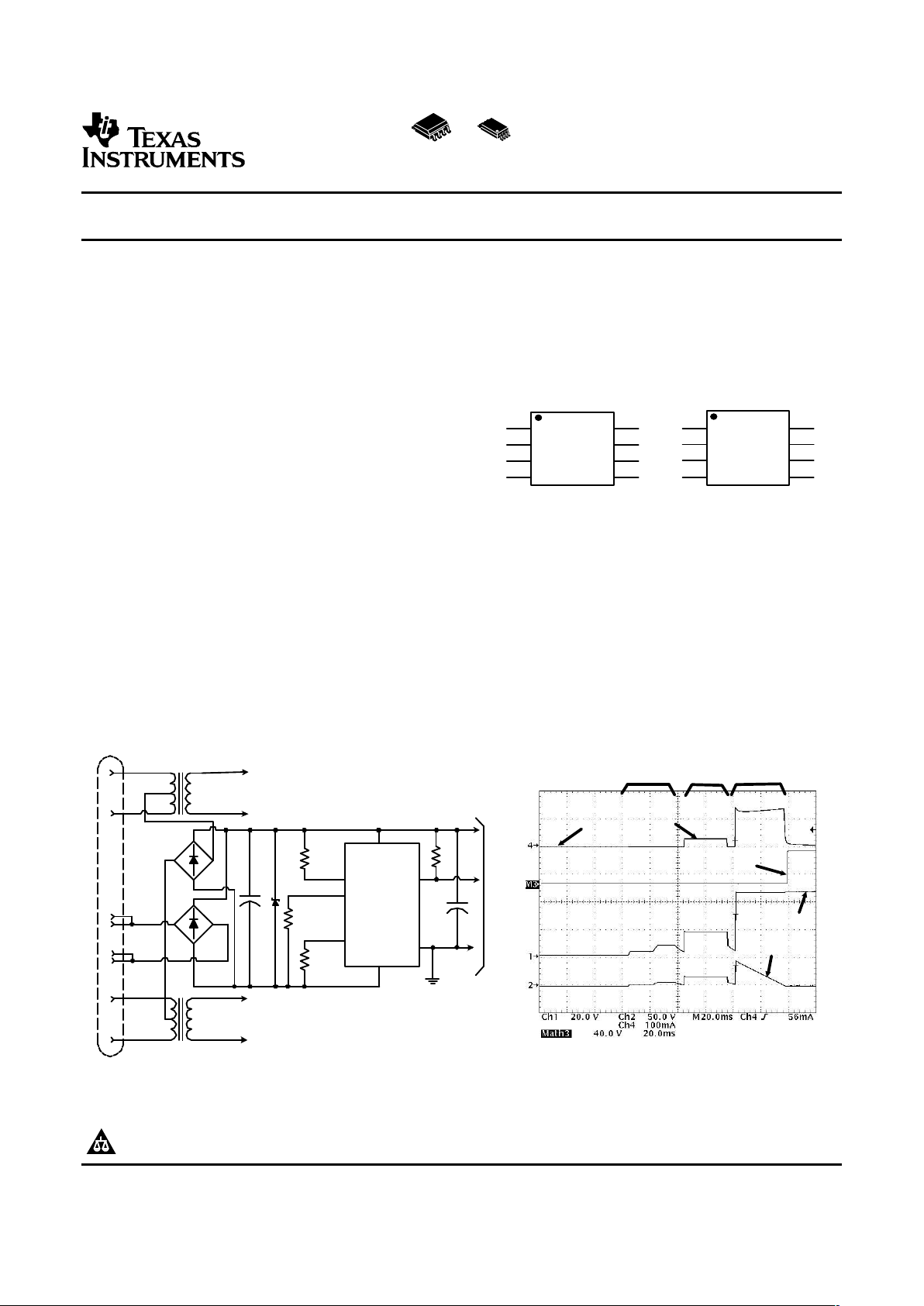
TPS2375
SMAJ58A
Data to
Ethernet PHY
VDD
VSS
CLASS
DET
RTN
PG
Data to
Ethernet
PHY
1
3
6
4
5
7
8
TO DC/DC
CONVERTER
ILIM
2
RJ−45
DF01S
2 Places
Note: Class 3 PD Depicted.
PG Pullup Resistor Is Optional.
TX
Pair
RX
Pair
Spare
Pair
Spare
Pair
V
DD
Input
Current
V
RTN
V
Detect Classify
Power Up & Inrush
Class 3
(PG-RTN)
100
k
100 V
100 F,
R
(DET)
24.9 k
1 %
R
(ILIM)
178 k
1 %
R
(ICLASS)
357
1 %
100 V
0.1F,
10 %
Note: All Voltages With Respect to VSS.
Current
TPS2375
TPS2376
TPS2377
SLVS525A – APRIL 2004 – REVISED SEPTEMBER 2004
IEEE 802.3af PoE POWERED DEVICE CONTROLLERS
• VoIP Phones
• Fully Supports IEEE 802.3af Specification
• WLAN Access Points
• Integrated 0.58- Ω , 100-V, Low-Side Switch
• Security Cameras
• 15-kV System Level ESD Capable
• Internet Appliances
• Supports Use of Low-Cost Silicon Rectifiers
• POS Terminals
• Programmable Inrush Current Control
• Fixed 450-mA Current Limit
• Fixed and Adjustable UVLO Options
• Open-Drain, Power-Good Reporting
• Overtemperature Protection
• Industrial Temperature Range: -40 ° C to 85 ° C
• 8-Pin SOIC and TSSOP Packages
These easy-to-use 8-pin integrated circuits contain all of the features needed to develop an IEEE 802.3af
compliant powered device (PD). The TPS2375 family is a second generation PDC (PD Controller) featuring
100-V ratings and a true open-drain, power-good function.
In addition to the basic functions of detection, classification and undervoltage lockout (UVLO), these controllers
include an adjustable inrush limiting feature. The TPS2375 has 802.3af compliant UVLO limits, the TPS2377 has
legacy UVLO limits, and the TPS2376 has a programmable UVLO with a dedicated input pin.
The TPS2375 family specifications incorporate a voltage offset of 1.5 V between its limits and the IEEE 802.3af
specifications to accommodate the required input diode bridges used to make the PD polarity insensitive.
Additional resources can be found on the TI Web site www.ti.com.
Figure 1. Typical Application Circuit and Startup Waveforms
Please be aware that an important notice concerning availability, standard warranty, and use in critical applications of Texas
Instruments semiconductor products and disclaimers thereto appears at the end of this data sheet.
PRODUCTION DATA information is current as of publication date.
Copyright © 2004, Texas Instruments Incorporated
Products conform to specifications per the terms of the Texas
Instruments standard warranty. Production processing does not
necessarily include testing of all parameters.
www.ti.com
AVAILABLE OPTIONS
ABSOLUTE MAXIMUM RATINGS
DISSIPATION RATING TABLE
(1)
TPS2375
TPS2376
TPS2377
SLVS525A – APRIL 2004 – REVISED SEPTEMBER 2004
This integrated circuit can be damaged by ESD. Texas Instruments recommends that all integrated
circuits be handled with appropriate precautions. Failure to observe proper handling and installation
procedures can cause damage.
ESD damage can range from subtle performance degradation to complete device failure. Precision
integrated circuits may be more susceptible to damage because very small parametric changes could
cause the device not to meet its published specifications.
UVLO THRESHOLDS (NOMINAL) PACKAGE
(1)
T
A
MARKING
TYPE LOW HIGH SO-8 TSSOP-8
802.3af 30.5 V 39.3 V TPS2375D TPS2375PW 2375
-40 ° C to 85 ° C Adjustable 1.93 V 2.49 V TPS2376D TPS2376PW 2376
Legacy 30.5 V 35.1 V TPS2377D TPS2377PW 2377
(1) Add an R suffix to the device type for tape and reel.
over operating free-air temperature range (unless otherwise noted)
(1)
, voltages are referenced to V
(VSS)
TPS237x
VDD, RTN, DET, PG
(2)
-0.3 V to 100 V
Voltage ILIM, UVLO -0.3 V to 10 V
CLASS -0.3 V to 12 V
RTN
(3)
0 to 515 mA
Current, sinking PG 0 to 5 mA
DET 0 to 1 mA
CLASS 0 to 50 mA
Current, sourcing
ILIM 0 to 1 mA
Human body model 2 kV
ESD Charged device model 500 V
System level (contact/air) at RJ-45
(4)
8/15 kV
T
J
Maximum junction temperature range Internally limited
T
stg
Storage temperature range -65 ° C to 150 ° C
Lead temperature 1,6 mm (1/16 inch) from case for 10 seconds - Green Packages 260 ° C
Lead temperature 1,6 mm (1/16 inch) from case for 10 seconds - Nongreen Packages 235 ° C
(1) Stresses beyond those listed under “absolute maximum ratings” may cause permanent damage to the device. These are stress ratings
only, and functional operation of the device at these or any other conditions beyond those indicated under “recommended operating
conditions” is not implied. Exposure to absolute–maximum–rated conditions for extended periods may affect device reliability.
(2) I
(RTN)
= 0
(3) SOA limited to V
(RTN)
= 80 V and I
(RTN)
= 515 mA.
(4) Surges applied to RJ-45 of Figure 1 between pins of RJ-45, and between pins and output voltage rails per EN61000-4-2, 1999.
POWER RATING
θJA(LOW-K) θJA(HIGH-K) (HIGH-K)
PACKAGE
° C/W ° C/W TA= 85 ° C
mW
D (SO-8) 238 150 266
PW (TSSOP-8) 258.5 159 251
(1) Tested per JEDEC JESD51. High-K is a (2 signal – 2 plane) test board and low-K is a double sided
board with minimum pad area and natural convection.
2
www.ti.com
RECOMMENDED OPERATING CONDITIONS
ELECTRICAL CHARACTERISTICS
TPS2375
TPS2376
TPS2377
SLVS525A – APRIL 2004 – REVISED SEPTEMBER 2004
MIN MAX UNIT
VDD, PG, RTN 0 57 V
Input voltage range
UVLO 0 5 V
Operating current range (sinking) RTN 0 350 mA
Classification resistor
(1)
CLASS 255 4420 Ω
R
(ILIM)
Inrush limit program resistor
(1)
62.5 500 k Ω
Sinking current PG 0 2 mA
T
J
Operating junction temperature -40 125 ° C
T
A
Operating free–air temperature -40 85 ° C
(1) Voltage should not be eternally applied to CLASS and ILIM.
V
(VDD)
= 48 V, R
(DET)
= 24.9 k Ω , R
(CLASS)
= 255 Ω , R
(ILIM)
= 178 k Ω , and –40 ° C ≤ TJ≤ 125 ° C, unless otherwise noted. Positive
currents are into pins. V
(UVLO)
= 0 V for classification and V
(UVLO)
= 5 V otherwise for the TPS2376. Typical values are at 25 ° C.
All voltages are with respect to VSS unless otherwise noted.
PARAMETER TEST CONDITIONS MIN TYP MAX UNIT
DETECTION
DET open, V
(VDD)
= V
(RTN)
= 1.9 V, measure
Offset current 0.3 3 µA
I
(VDD)
+ I
(RTN)
DET open, V
(VDD)
= V
(RTN)
= 10.1 V, measure
Sleep current 4 12 µA
I
(VDD)
+ I
(RTN)
DET leakage current V
(DET)
= V
(VDD)
= 57 V, measure I
(DET)
0.1 5 µA
V
(RTN)
= V
(VDD)
, V
(VDD)
= 1.4 V 53.7 56 58.3 µA
R
(DET)
= 24.9 k Ω ,
Detection current
measure I
(VDD)
+ I
(RTN)
+
V
(VDD)
= 10.1 V 395 410 417 µA
I
(DET)
CLASSIFICATION
R
(CLASS)
= 4420 Ω , 13 ≤ V
(VDD)
≤ 21 V 2.2 2.4 2.8
R
(CLASS)
= 953 Ω , 13 ≤ V
(VDD)
≤ 21 V 10.3 10.6 11.3
I
(CLASS)
Classification current
(1)
R
(CLASS)
= 549 Ω , 13 ≤ V
(VDD)
≤ 21 V 17.7 18.3 19.5 mA
R
(CLASS)
= 357 Ω , 13 ≤ V
(VDD)
≤ 21 V 27.1 28.0 29.5
R
(CLASS)
= 255 Ω , 13 ≤ V
(VDD)
≤ 21 V 38.0 39.4 41.2
V
(CL_ON)
Classification lower threshold Regulator turns on, V
(VDD)
rising 10.2 11.3 13.0 V
V
(CU_OFF)
Regulator turns off, V
(VDD)
rising 21 21.9 23 V
Classification upper threshold
V
(CU_H)
Hysteresis 0.5 0.78 1 V
Leakage current V
(CLASS)
= 0 V, V
(VDD)
= 57 V 1 µA
PASS DEVICE
r
DS(on)
On resistance I
(RTN)
= 300 mA 0.58 1.0 Ω
V
(VDD)
= V
(RTN)
= 30 V, 15
Leakage current µA
V
(UVLO)
= 0 V (TPS2376)
Current limit V
(RTN)
= 1 V 405 461 515 mA
I
(LIM)
Inrush limit V
(RTN)
= 2 V, R
(ILIM)
= 178 k Ω 100 130 180 mA
V
(RTN)
falling, R
(ILIM)
= 178 k Ω , inrush 85% 91% 100%
Inrush current termination
(2)
state → normal operation
R
(ILIM)
= 69.8 k Ω , V
(RTN-VSS)
= 5 V, 15 25
Current rise time into inrush I
(RTN)
= 30 mA → 300 mA, V
(VDD)
increasing µs
past upper UVLO
Apply load ∞ Ω → 20 Ω , time measured to 2 2.5
Current limit response time µs
I
(RTN)
= 45 mA
Leakage current, ILIM V
(VDD)
= 15 V, V
(UVLO)
= 0 V 1 µA
(1) Classification is tested with exact resistor values. A 1% tolerance classification resistor assures compliance with IEEE 802.3af limits.
(2) This parameter specifies the RTN current value, as a percentage of the steady state inrush current, below which it must fall to make PG
assert (open-drain).
3
www.ti.com
TPS2375
TPS2376
TPS2377
SLVS525A – APRIL 2004 – REVISED SEPTEMBER 2004
ELECTRICAL CHARACTERISTICS (continued)
V
(VDD)
= 48 V, R
(DET)
= 24.9 k Ω , R
(CLASS)
= 255 Ω , R
(ILIM)
= 178 k Ω , and –40 ° C ≤ TJ≤ 125 ° C, unless otherwise noted. Positive
currents are into pins. V
(UVLO)
= 0 V for classification and V
(UVLO)
= 5 V otherwise for the TPS2376. Typical values are at 25 ° C.
All voltages are with respect to VSS unless otherwise noted.
PARAMETER TEST CONDITIONS MIN TYP MAX UNIT
PG
Latchoff voltage threshold rising V
(RTN)
rising 9.5 10.0 10.5 V
PG deglitch Delay rising and falling PG 75 150 225 µs
I
(PG)
= 2 mA, V
(RTN)
= 34 V, 0.12 0.4
V
V
(VDD)
= 38 V, V
(RTN)
falling
Output low voltage
I
(PG)
= 2 mA, V
(RTN)
= 0 V, V
(VDD)
= 25 V, for 0.12 0.4
V
TPS2376 V
(UVLO)
= 0 V
Leakage current V
(PG)
= 57 V, V
(RTN)
= 0 V 0.1 1 µA
UVLO
V
(UVLO_R)
V
(VDD)
rising 38.4 39.3 40.4
V
(UVLO_F)
TPS2375 Voltage at VDD V
(VDD)
falling 29.6 30.5 31.5 V
Hysteresis 8.3 8.8 9.1
V
(VDD)
rising 2.43 2.49 2.57
TPS2376 Voltage at UVLO V
(VDD)
falling 1.87 1.93 1.98 V
Hysteresis 0.53 0.56 0.58
V
(VDD)
rising 34.1 35.1 36.0
TPS2377 Voltage at VDD V
(VDD)
falling 29.7 30.5 31.4 V
Hysteresis 4.3 4.5 4.8
TPS2376 Input leakage, UVLO V
(UVLO)
= 0 V to 5 V -1 1 µA
THERMAL SHUTDOWN
Shutdown temperature Temperature rising 135 ° C
Hysteresis 20 ° C
BIAS CURRENT
Operating current I
(VDD)
240 450 µA
4
www.ti.com
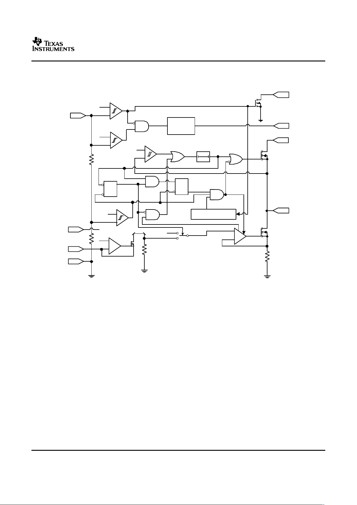
DEVICE INFORMATION
−
+
10 V
Regulator
Thermal Shutdown,
Counter, and Latch
QS
R
−
+
−
+
3
2
12 V
22 V
1.5 V
& 10 V
2.5 V
−
+
VDD
RTN
45 mV
CLASS
DET
Current
Limit Amp.
UVLO
Comp.
EN
Delay
QS
R
5
8
6
PG
−
+
0 = Inrush
0 = Fault
1 = Limiting
PG Comparator
Detection
Comparator
Classification
Comparator
0
1
7
UVLO
’76 Only
−
+
2.5 V
1
ILIM
1:1
4
VSS
See
Note
Note: For The TPS2376, The UVLO Comparator
Connects To The UVLO Pin And Not The UVLO
Divider.
Current
Mirror
1 kOhms
0.08
Ohms
150 uS
TPS2375
TPS2376
TPS2377
SLVS525A – APRIL 2004 – REVISED SEPTEMBER 2004
FUNCTIONAL BLOCK DIAGRAM
5
www.ti.com
Detailed Pin Description
I
(LIM)
25000
R
(ILIM)
(1)
TPS2375
TPS2376
TPS2377
SLVS525A – APRIL 2004 – REVISED SEPTEMBER 2004
DEVICE INFORMATION (continued)
TERMINAL FUNCTIONS
PIN NUMBER
PIN NAME I/O DESCRIPTION
TPS2375/77 TPS2376
Connect a resistor from ILIM to VSS to set the start-up inrush current limit.
ILIM 1 1 O The equation for calculating the resistor is shown in the detailed pin
description section for ILIM.
Connect a resistor from CLASS to VSS to set the classification of the
CLASS 2 2 O powered device (PD). The IEEE classification levels and corresponding
resistor values are shown in Table 1 .
Connect a 24.9-k Ω detection resistor from DET to VDD for a valid PD
DET 3 3 O
detection.
VSS 4 4 I Return line on the source side of the TPS2375 from the PSE.
Switched output side return line used as the low-side reference for the
RTN 5 5 O
TPS2375 load.
PG 6 6 O Open-drain, power-good output; active high.
Used only on the TPS2376. Connect a resistor divider from VDD to VSS to
UVLO - 7 I
implement the adjustable UVLO feature of the TPS2376.
NC 7 - No connection
VDD 8 8 I Positive line from the rectified PSE provided input.
The following descriptions refer to the schematic of Figure 1 and the functional block diagram.
ILIM: A resistor from this pin to VSS sets the inrush current limit per Equation 1 :
where ILIM is the desired inrush current value, in amperes, and R
(ILIM)
is the value of the programming resistor
from ILIM to VSS, in ohms. The practical limits on R
(ILIM)
are 62.5 k Ω to 500 k Ω . A value of 178 k Ω is
recommended for compatibility with legacy PSEs.
Inrush current limiting prevents current drawn by the bulk capacitor from causing the line voltage to sag below
the lower UVLO threshold. Adjustable inrush current limiting allows the use of arbitrarily large capacitors and also
accommodates legacy systems that require low inrush currents.
The ILIM pin must not be left open or shorted to VSS.
CLASS: Classification is implemented by means of an external resistor, R
(CLASS)
, connected between CLASS
and VSS. The controller draws current from the input line through R
(CLASS)
when the input voltage lies between
13 V and 21 V. The classification currents specified in the electrical characteristics table include the bias current
flowing into VDD and any RTN leakage current.
Table 1. CLASSIFICATION
CLASS PD POWER (W) R
(CLASS)
( Ω ) 802.3af LIMITS (mA) NOTE
0 0.44 – 12.95 4420 ± 1% 0 - 4 Default class
1 0.44 – 3.84 953 ± 1% 9 - 12
2 3.84 – 6.49 549 ± 1% 17 - 20
3 6.49 – 12.95 357 ± 1% 26 - 30
4 - 255 ± 1% 36 - 44 Reserved for future use
The CLASS pin must not be shorted to ground.
DET: Connect a resistor, R
(DET)
, between DET and VDD. This resistor should equal 24.9 k Ω , ± 1% for most
applications. R
(DET)
is connected across the input line when V
(VDD)
lies between 1.4 V and 11.3 V, and is
disconnected when the line voltage exceeds this range to conserve power. This voltage range has been chosen
to allow detection with two silicon rectifiers between the controller and the RJ-45 connector.
6
www.ti.com
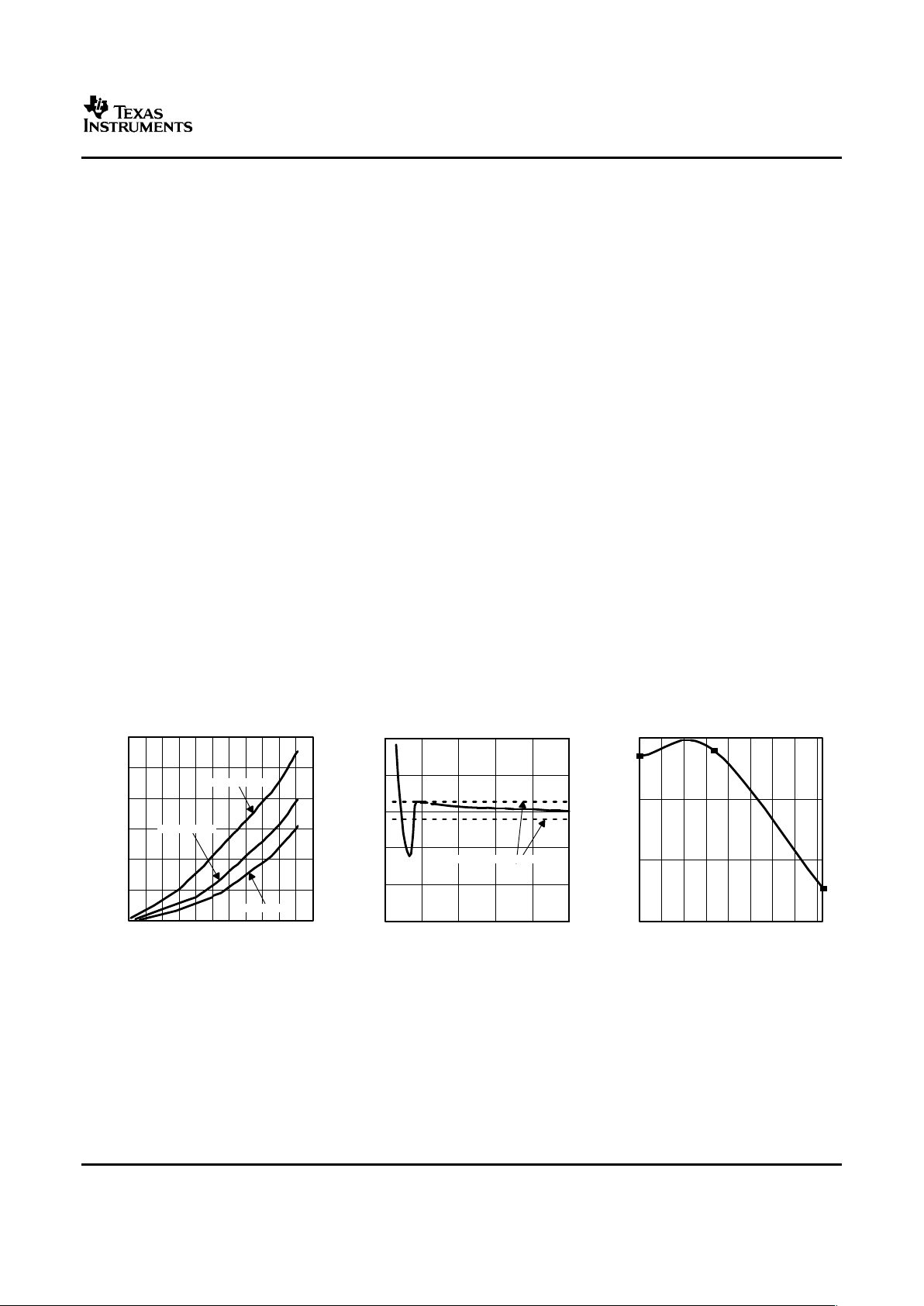
TYPICAL CHARACTERISTICS
11.0
11.1
11.2
11.3
−40 −20 0 20 40 60 80 100 120
Classification Turnon Voltage − V
TA − Free-Air Temperature − °C
0
1
2
3
4
5
6
0 1 2 3 4 5 6 7 8 9 10 11
TA = 125°C
TA = 25°C
TA = −40°C
V
(VDD)
− V
Current − Aµ
10
15
20
25
30
35
1 3 5 7 9 11
Specification Limits
V
(PI)
− V
Resistance − kΩ
TPS2375
TPS2376
TPS2377
SLVS525A – APRIL 2004 – REVISED SEPTEMBER 2004
VSS: This is the input supply negative rail that serves as a local ground to the TPS2375.
RTN: This pin provides the switched negative power rail used by the downstream circuits. The operational and
inrush current limit control current into the pin. The PG circuit monitors the RTN voltage and also uses it as the
return for the PG pin pulldown transistor. The internal MOSFET body diode clamps VSS to RTN when voltage is
present between VDD and RTN and the PoE input is not present.
PG: This pin goes to a high resistance state when the internal MOSFET that feeds the RTN pin is enabled, and
the device is not in inrush current limiting. In all other states except detection, the PG output is pulled to RTN by
the internal open-drain transistor. Performance is assured with at least 4 V between VDD and RTN.
PG is an open-drain output; therefore, it may require a pullup resistor or other interface.
UVLO: This pin is specific to the TPS2376; it is not internally connected on the TPS2375 and TPS2377. The
UVLO pin is used with an external resistor divider between VDD and VSS to set the upper and lower UVLO
thresholds. The hysteresis, as measured as a percentage of the upper UVLO, is the same as the TPS2375.
The TPS2376 enables the output when V
(UVLO)
exceeds the upper UVLO threshold. When current begins to flow,
VDD sags due to cable resistance and the dynamic resistance of the input diodes. The lower UVLO threshold
must be below the lowest voltage that the input reaches.
The TPS2376 implements adjustable UVLO thresholds, but is otherwise functionally equivalent to the TPS2375.
The TPS2375 offers fixed UVLO thresholds designed to maximize hysteresis while maintaining compatibility with
the IEEE 802.3af standard. The TPS2377 offers fixed UVLO thresholds optimized for use with legacy PoE
systems.
VDD: This is the positive input supply to the TPS2375, which is also common to downstream load circuits. This
pin provides operating power and allows the controller to monitor the line voltage to determine the mode of
operation.
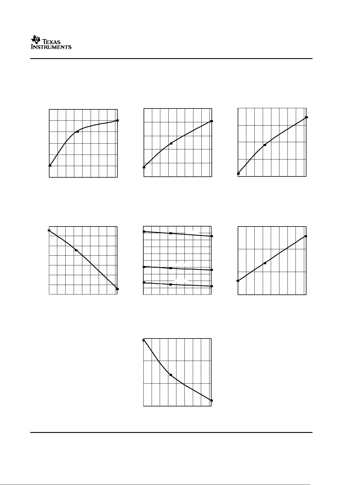
Graphs over temperature are interpolations between the marked data points.
I
(VDD)
+ I
(RTN)
IN DETECTION PD DETECTION RESISTANCE CLASSIFICATION TURNON
vs VOLTAGE
V
(PI)
vs
TEMPERATURE
Figure 2. Figure 3. Figure 4.
7
www.ti.com
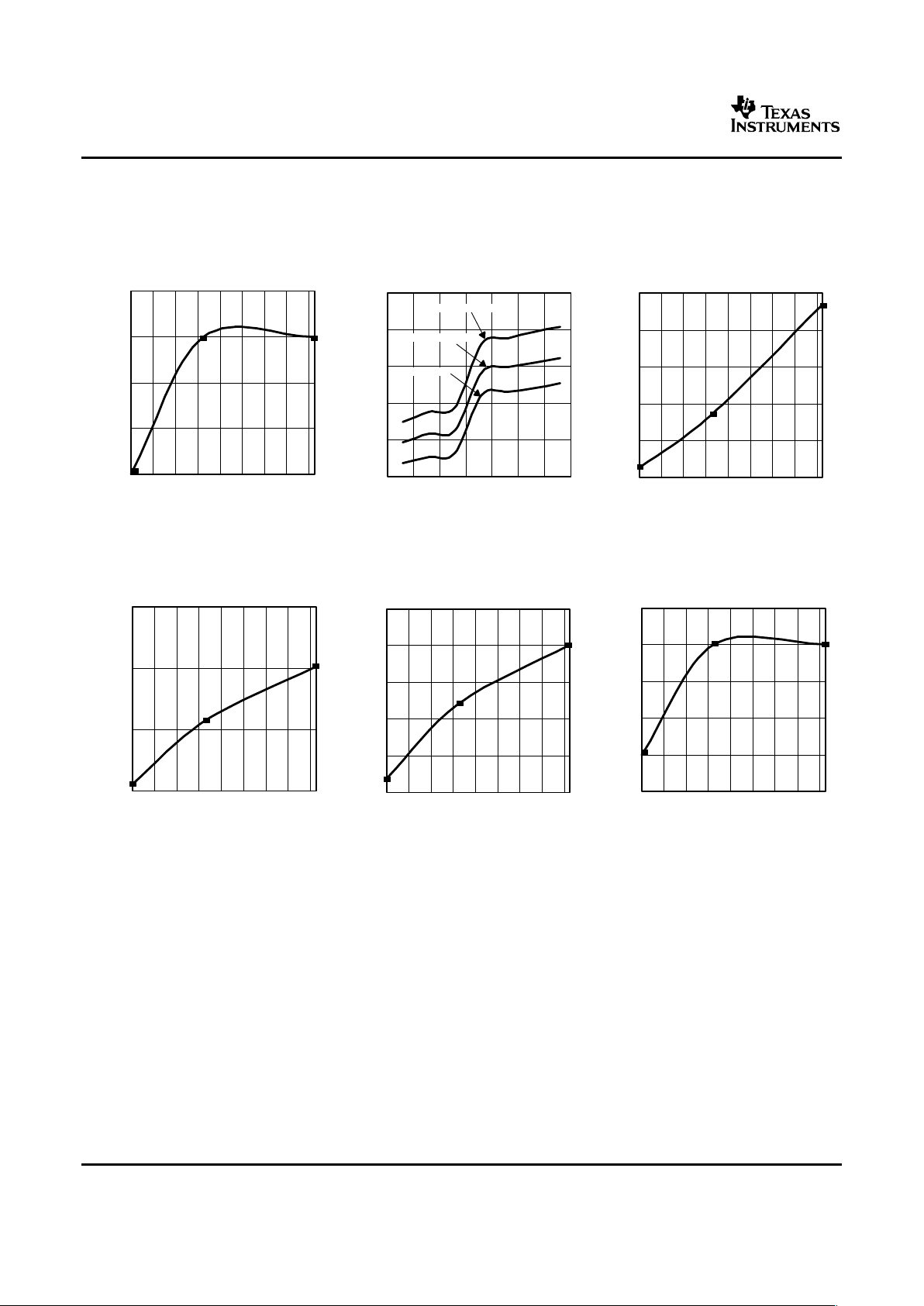
21.90
21.91
21.92
21.93
21.94
−40 −20 0 20 40 60 80 100 120
Classification Turnoff Voltage − V
TA − Free-Air Temperature − °C
0.100
0.150
0.200
0.250
0.300
0.350
22 27 32 37 42 47 52 57
VDD − V
I
(VDD)
− mA
TA = 125°C
TA = 25°C
TA = −40°C
0.4
0.5
0.6
0.7
0.8
0.9
−40 −20 0 20 40 60 80 100 120
Pass Device Resistance − Ω
TA − Free-Air Temperature − °C
39.2
39.3
39.4
39.5
−40 −20 0 20 40 60 80 100 120
T
A
− Free-Air Temperature − °C
VDD − V
2.484
2.485
2.486
2.487
2.488
2.489
−40 −20 0 20 40 60 80 100 120
(UVLO)
TA − Free-Air Temperature − °C
V − V
30.40
30.44
30.48
30.52
30.56
30.60
−40 −20 0 20 40 60 80 100 120
T
A
− Free-Air Temperature − °C
VDD − V
TPS2375
TPS2376
TPS2377
SLVS525A – APRIL 2004 – REVISED SEPTEMBER 2004
TYPICAL CHARACTERISTICS (continued)
Graphs over temperature are interpolations between the marked data points.
CLASSIFICATION TURNOFF I
(VDD)
CURRENT PASS DEVICE
VOLTAGE vs RESISTANCE
vs VDD vs
TEMPERATURE TEMPERATURE
Figure 5. Figure 6. Figure 7.
TPS2375 TPS2375 TPS2376
UVLO RISING UVLO FALLING UVLO RISING
vs vs vs
TEMPERATURE TEMPERATURE TEMPERATURE
Figure 8. Figure 9. Figure 10.
8
www.ti.com
30.45
30.50
30.55
30.60
30.65
−40 −20 0 20 40 60 80 100 120
T
A
− Free-Air Temperature − °C
VDD − V
34.95
35.00
35.05
35.10
35.15
35.20
−40 −20 0 20 40 60 80 100 120
T
A
− Free-Air Temperature − °C
VDD − V
1.923
1.924
1.925
1.926
1.927
1.928
1.929
−40 −20 0 20 40 60 80 100 120
T
A
− Free-Air Temperature − °C
(UVLO)
V − V
425
430
435
440
−40 −20 0 20 40 60 80 100 120
T
A
− Free-Air Temperature − °C
I
(RTN)
− mA
90.5
91.0
91.5
92.0
92.5
93.0
93.5
94.0
−40 −20 0 20 40 60 80 100 120
Percent of Inrush Limit Current
TA − Free-Air Temperature − °C
100
125
150
175
200
225
250
275
300
325
350
−40 −20 0 20 40 60 80 100 120
I
(ILIM)
− mA
TA − Free-Air Temperature − °C
75 kΩ
125 kΩ
178 kΩ
120
140
160
180
−40 −20 0 20 40 60 80 100 120
PG Deglitch Period −
sµ
TA − Free-Air Temperature − °C
TPS2375
TPS2376
TPS2377
SLVS525A – APRIL 2004 – REVISED SEPTEMBER 2004
TYPICAL CHARACTERISTICS (continued)
Graphs over temperature are interpolations between the marked data points.
TPS2376 TPS2377 TPS2377
UVLO FALLING UVLO RISING UVLO FALLING
vs vs vs
TEMPERATURE TEMPERATURE TEMPERATURE
Figure 11. Figure 12. Figure 13.
INRUSH STATE TERMINATION INRUSH CURRENT CURRENT LIMIT
THRESHOLD vs vs
vs TEMPERATURE TEMPERATURE
TEMPERATURE
Figure 14. Figure 15. Figure 16.
PG DEGLITCH PERIOD
vs
TEMPERATURE
Figure 17.
9
 Loading...