

Texas Instruments TPS2330IPWR, TPS2330IPW, TPS2330IDR, TPS2330ID, TPS2331IPWR Datasheet
...
TPS2330, TPS2331
SINGLE HOT SWAP POWER CONTROLLER WITH
CIRCUIT BREAKER AND POWER-GOOD REPORTING
SLVS277A – MARCH 2000– REVISED APRIL 2000
1
POST OFFICE BOX 655303 • DALLAS, TEXAS 75265
features
D
Single-Channel High-Side MOSFET Driver
D
Input Voltage: 3 V to 13 V
D
Inrush Current Limiting With dv/dt Control
D
Circuit-Breaker Control With Programmable
Current Limit and Transient Timer
D
Power-Good Reporting With Transient
Filter
D
CMOS- and TTL-Compatible Enable Input
D
Low 5-µA Standby Supply Current ...Max
D
Available in 14-Pin SOIC and TSSOP
Package
D
–40°C to 85°C Ambient Temperature Range
D
Electrostatic Discharge Protection
applications
D
Hot-Swap/Plug/Dock Power Management
D
Hot-Plug PCI, Device Bay
D
Electronic Circuit Breaker
description
The TPS2330 and TPS2331 are single-channel hot-swap controllers that use external N-channel MOSFETs
as high-side switches in power applications. Features of these devices, such as overcurrent protection (OCP),
inrush-current control, output-power status reporting, and separation of load transients from actual load
increases, are critical requirements for hot-swap applications.
The TPS2330/31 devices incorporate undervoltage lockout (UVLO) and power-good (PG) reporting to ensure
the device is off at start-up and confirm the status of the output voltage rails during operation. An internal charge
pump, capable of driving multiple MOSFET s, provides enough gate-drive voltage to fully enhance the N-channel
MOSFET s. The charge pump controls both the rise times and fall times (dv/dt) of the MOSFET s, reducing power
transients during power up/down. The circuit-breaker functionality combines the ability to sense overcurrent
conditions with a timer function; this allows designs such as DSPs, that may have high peak currents during
power-state transitions, to disregard transients for a programmable period.
AVAILABLE OPTIONS
PIN
PACKAGES
TAHOT-SWAP CONTROLLER DESCRIPTION
COUNT
ENABLE ENABLE
Dual-channel with independent OCP and adjustable PG 20 TPS2300IPW TPS2301IPW
Dual-channel with interdependent OCP and adjustable PG 20 TPS2310IPW TPS2311IPW
–40°C to 85°C
Dual-channel with independent OCP 16
TPS2320ID
TPS2320IPW
TPS2321ID
TPS2321IPW
Single-channel with OCP and adjustable PG 14
TPS2330ID
TPS2330IPW
TPS2331ID
TPS2331IPW
†
The packages are available left-end taped and reeled (indicated by the R suffix on the device type; e.g., TPS2331IPWR).
Copyright 2000, Texas Instruments Incorporated
PRODUCTION DATA information is current as of publication date.
Products conform to specifications per the terms of Texas Instruments
standard warranty. Production processing does not necessarily include
testing of all parameters.
Please be aware that an important notice concerning availability, standard warranty, and use in critical applications of
Texas Instruments semiconductor products and disclaimers thereto appears at the end of this data sheet.
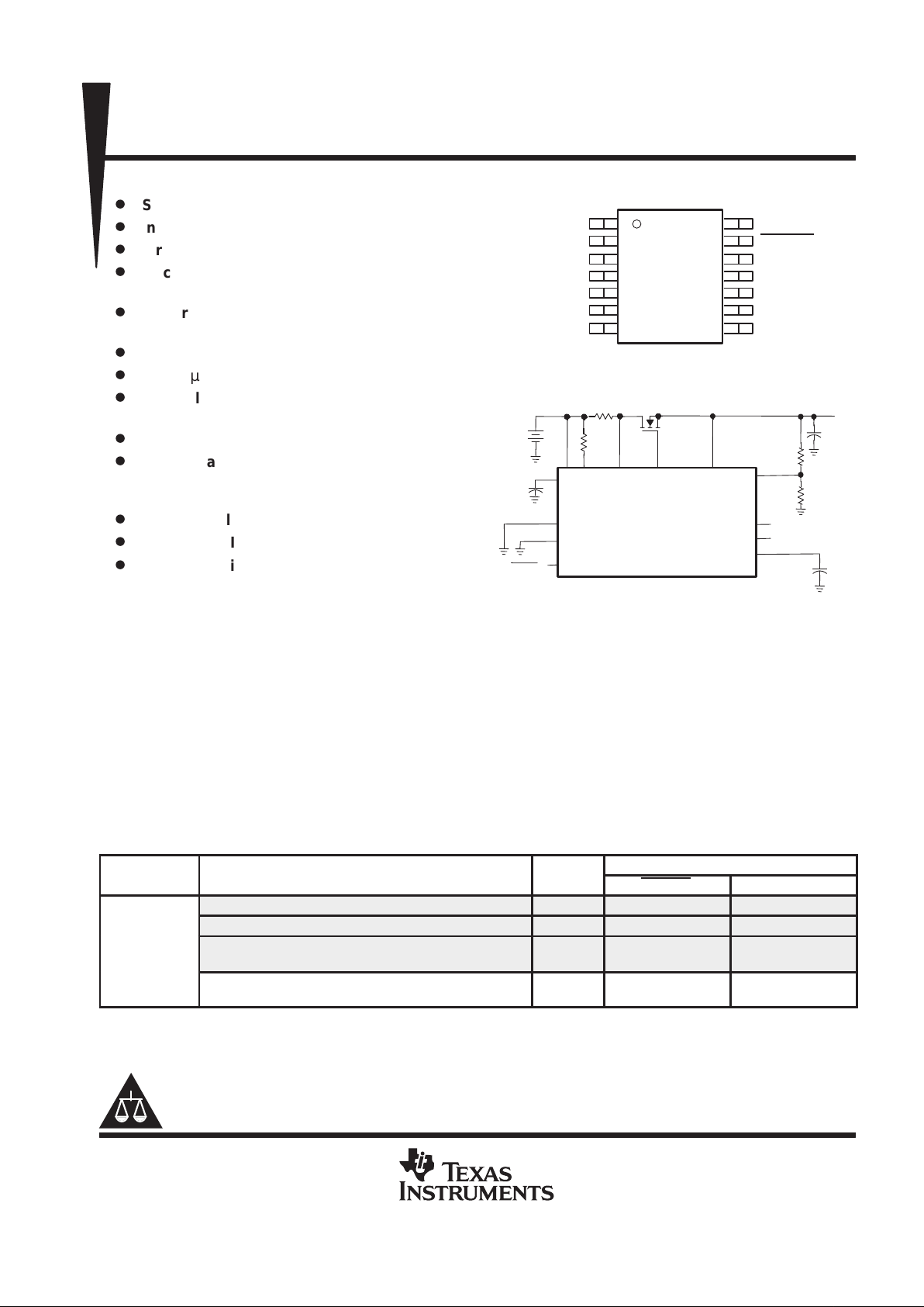
typical application
NOTE: Terminal 13 is active high on TPS2331.
VREG
IN
ISET
ISENSE
GATE
DISCH
VSENSE
PWRGD
FAULT
TIMER
ENABLE
DGND
AGND
VIN
3 V – 13 V
TPS2330
+
V
O
1
2
3
4
5
6
7
14
13
12
11
10
9
8
GATE
DGND
TIMER
VREG
VSENSE
AGND
ISENSE
DISCH
ENABLE
PWRGD
FAULT
ISET
AGND
IN
D OR PW PACKAGE
(TOP VIEW)
TPS2330, TPS2331
SINGLE HOT SWAP POWER CONTROLLER WITH
CIRCUIT BREAKER AND POWER-GOOD REPORTING
SLVS277A – MARCH 2000– REVISED APRIL 2000
2
POST OFFICE BOX 655303 • DALLAS, TEXAS 75265
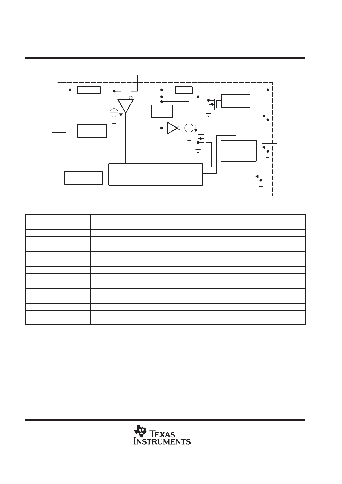
functional block diagram
PREREG
UVLO and
Power-Up
IN ISET ISENSE GATE
Clamp
Charge
Pump
75 µA
Pulldown FET
Circuit Breaker
dv/dt Rate
Protection
20-µs Deglitch
DISCH
Logic
VSENSE
PWRGD
FAULT
TIMER
Circuit
Breaker
VREG
50-µs Deglitch
AGND
DGND
ENABLE
50 µA
Terminal Functions
TERMINAL
NAME NO.
I/O
DESCRIPTION
AGND 6,9 I Analog ground, connects to DGND as close as possible
DGND 2 I Digital ground
DISCH 14 O Discharge transistor
ENABLE/ ENABLE 13 I Active low (TPS2330) or active high enable (TPS2331)
FAULT 11 O Overcurrent fault, open-drain output
GATE 1 O Connects to gate of high-side MOSFET
IN 8 I Input voltage
ISENSE 7 I Current-sense input
ISET 10 I Adjusts circuit-breaker threshold with resistor connected to IN
PWRGD 12 O Open-drain output, asserted low when VSENSE voltage is less than reference.
TIMER 3 O Adjusts circuit-breaker deglitch time
VREG 4 O Connects to bypass capacitor, for stable operation
VSENSE 5 I Power-good sense input

TPS2330, TPS2331
SINGLE HOT SWAP POWER CONTROLLER WITH
CIRCUIT BREAKER AND POWER-GOOD REPORTING
SLVS277A – MARCH 2000– REVISED APRIL 2000
3
POST OFFICE BOX 655303 • DALLAS, TEXAS 75265
detailed description
DISCH – DISCH should be connected to the source of the external N-channel MOSFET transistor connected
to GATE. This pin discharges the load when the MOSFET transistor is disabled. They also serve as
reference-voltage connection for internal gate-voltage-clamp circuitry.
ENABLE or ENABLE – ENABLE for TPS2330 is active low. ENABLE for TPS2331 is active high. When the
controller is enabled, GA TE voltage will power up to turn on the external MOSFETs. When the ENABLE
pin is
pulled high for TPS2330 or the ENABLE pin is pulled low for TPS2331 for more than 50 µs, the gate of the
MOSFET is discharged at a controlled rate by a current source, and a transistor is enabled to discharge the
output bulk capacitance. In addition, the device turns on the internal regulator PREREG (see VREG) when
enabled and shuts down PREREG when disabled so that total supply current is much less than 5 µA.
FAULT – FAULT is an open-drain overcurrent flag output. When an overcurrent condition is sustained long
enough to charge TIMER to 0.5 V, the device latches off and pulls FAULT low.
GATE – GA TE connects to the gate of the external N-channel MOSFET transistor. When the device is enabled,
internal charge-pump circuitry pulls this pin up by sourcing approximately 15 µA. The turnon slew rates depend
upon the capacitance present at the GATE terminal. If desired, the turnon slew rates can be further reduced
by connecting capacitors between this pin and ground. These capacitors also reduce inrush current and protect
the device from false overcurrent triggering during powerup. The charge-pump circuitry will generate
gate-to-source voltages of 9 V–12 V across the external MOSFET transistor.
IN – IN should be connected to the power source driving the external N-channel MOSFET transistor connected
to GA TE. The TPS2330/31 draws its operating current from IN, and will remain disabled until the IN power supply
has been established. The device has been constructed to support 3-V, 5-V, or 12-V operation.
ISENSE, ISET – ISENSE in combination with ISET implements overcurrent sensing for GATE. ISET sets the
magnitude of the current that generates an overcurrent fault, through a external resistor connected to ISET . An
internal current source draws 50 µA from ISET . With a sense resistor from IN to ISENSE, which is also connected
to the drain of the external MOSFET , the voltage on the sense resistor reflects the load current. An overcurrent
condition is assumed to exist if ISENSE is pulled below ISET.
PWRGD – PWRGD signals the presence of undervoltage conditions on VSENSE. The pin is an open-drain
output and is pulled low during an undervoltage condition. To minimize erronous PWRGD responses from
transients on the voltage rail, the voltage sense circuit incorporates a 20-µs deglitch filter. When VSENSE is
lower than the reference voltage (about 1.23 V), PWRGD will be active low to indicate an undervoltage condition
on the power-rail voltage.
TIMER – A capacitor on TIMER sets the time during which the power switch can be in overcurrent before turning
off. When the overcurrent protection circuits sense an excessive current, a current source is enabled which
charges the capacitor on TIMER. Once the voltage on TIMER reaches approximately 0.5 V , the circuit-breaker
latch is set and the power switch is latched off. Power must be recycled or the ENABLE pin must be toggled
to restart the controller. In high-power or high-temperature applications, a minimum 50-pF capacitor is strongly
recommended from TIMER to ground, to prevent any false triggering.
VREG – The VREG pin is the output of an internal low-dropout voltage regulator. This regulator draws current
from IN. A 0.1-µF ceramic capacitor should be connected between VREG and ground. VREG can be connected
to IN or to a separated power supply through a low-resistance resistor. However, the voltage on VREG must
be less than 5.5 V.
VSENSE – VSENSE can be used to detect undervoltage conditions on external circuitry. If VSENSE senses
a voltage below approximately 1.23 V, PWRGD is pulled low.
TPS2330, TPS2331
SINGLE HOT SWAP POWER CONTROLLER WITH
CIRCUIT BREAKER AND POWER-GOOD REPORTING
SLVS277A – MARCH 2000– REVISED APRIL 2000
4
POST OFFICE BOX 655303 • DALLAS, TEXAS 75265
absolute maximum ratings over operating free-air temperature (unless otherwise noted)
†
Input voltage range: V
I(IN)
, V
I(ISENSE)
, V
I(VSENSE),VI(ISET)
, V
I(ENABLE)
–0.3 V to 15 V. . . . . . . . . . . . . . .
Output voltage range: V
O(GATE)
–0.3 V to 30 V. . . . . . . . . . . . . . . . . . . . . . . . . . . . . . . . . . . . . . . . . . . . . . . . . .
V
O(DISCH)
, V
O(PWRGD)
, V
O(FAULT)
, V
O(VREG)
, V
O(TIMER)
–0.3 V to 15V. . . . . . .
Sink current range: I
GATE
, I
DISCH
0 mA to 100 mA. . . . . . . . . . . . . . . . . . . . . . . . . . . . . . . . . . . . . . . . . . . . . . . .
I
PWRGD
, I
TIMER
, I
FAULT
0 mA to 10 mA. . . . . . . . . . . . . . . . . . . . . . . . . . . . . . . . . . . . . . . .
Operating virtual junction temperature range, TJ –40°C to 100°C. . . . . . . . . . . . . . . . . . . . . . . . . . . . . . . . . . . . .
Storage temperature range, T
stg
–55°C to 150°C. . . . . . . . . . . . . . . . . . . . . . . . . . . . . . . . . . . . . . . . . . . . . . . . . . .
Lead temperature 1,6 mm (1/16 inch) from case for 10 seconds 260°C. . . . . . . . . . . . . . . . . . . . . . . . . . . . . . .
†
Stresses beyond those listed under “absolute maximum ratings” may cause permanent damage to the device. These are stress ratings only, and
functional operation of the device at these or any other conditions beyond those indicated under “recommended operating conditions” is not
implied. Exposure to absolute-maximum-rated conditions for extended periods may affect device reliability.
NOTE 1: All voltages are respect to DGND.
DISSIPATION RATING T ABLE
PACKAGE
TA ≤ 25°C
POWER RATING
DERATING FACTOR
ABOVE TA = 25°C
TA = 70°C
POWER RATING
TA = 85°C
POWER RATING
PW-14 755 mW 10.07 mW/°C 302 mW 151 mW
D-14 613 mW 8.18 mW/°C 245 mW 123 mW
recommended operating conditions
MIN NOM MAX UNIT
Input voltage, V
I
V
I(IN)
, V
I(ISENSE)
, V
I(VSENSE)
, V
I(ISET)
3 13 V
VREG voltage, V
O(VREG)
, when VREG is directly connected to IN 2.95 5.5 V
Operating virtual junction temperature, T
J
–40 100 °C
TPS2330, TPS2331
SINGLE HOT SWAP POWER CONTROLLER WITH
CIRCUIT BREAKER AND POWER-GOOD REPORTING
SLVS277A – MARCH 2000– REVISED APRIL 2000
5
POST OFFICE BOX 655303 • DALLAS, TEXAS 75265
electrical characteristics over recommended operating temperature range (–40°C < TA < 85°C),
3 V ≤ V
I(IN)
≤13 V (unless otherwise noted)
general
PARAMETER TEST CONDITIONS MIN TYP MAX UNIT
p
V
I(ENABLE)
= 5 V (TPS2331), 0.5 1 mA
I
I(IN)
Input current, IN
V
I(ENABLE)
= 0 V (TPS2330) 75 200
I
I(stby)
Standby current (sum of currents into IN ISENSE and ISET)
V
I(ENABLE)
= 0 V (TPS2331),
V
I(ENABLE
)
= 5 V (TPS2330)
5 µA
GATE
PARAMETER TEST CONDITIONS MIN TYP MAX UNIT
V
G(GATE_3V)
V
I(IN)
= 3 V 9 11.5
V
G(GATE_4.5V)
Gate voltage
I
I(GATE)
=
500 nA
,
DISCH open
V
I(IN)
= 4.5 V 10.5 14.5
V
V
G(GATE_10.8V)
DISCH oen
V
I(IN)
= 10.8 V 16.8 21
V
C(GATE)
Clamping voltage, GATE to
DISCH
9 10 12 V
I
S(GATE)
Source current, GATE
3 V ≤ V
I(IN)
≤ 13.2 V, 3 V ≤ V
O(VREG)
≤ 5.5 V,
V
I(GATE)
= V
I(IN)
+ 6 V
10 14 20 µA
Sink current, GATE
3 V ≤ V
I(IN)
≤ 13.2 V, 3 V ≤ V
O(VREG)
≤ 5.5 V,
V
I(GATE)
= V
I(IN)
50 75 100 µA
V
I(IN)
= 3 V 0.5
t
r(GATE)
Rise time, GATE Cg to GND = 1 nF (see Note 2)
V
I(IN)
= 4.5 V 0.6
ms
()
g
V
I(IN)
= 10.8 V 1
V
I(IN)
= 3 V 0.1
t
f(GATE)
Fall time, GATE Cg to GND = 1 nF (see Note 2)
V
I(IN)
= 4.5 V 0.12
ms
()
g
V
I(IN)
= 10.8 V 0.2
NOTE 2: Specified, but not production tested.
TIMER
PARAMETER TEST CONDITIONS MIN TYP MAX UNIT
V
OT(TIMER)
Threshold voltage, TIMER 0.4 0.5 0.6 V
Charge current, TIMER V
I(TIMER)
= 0 V 35 50 65 µA
Discharge current, TIMER V
I(TIMER)
= 1 V 1 2.5 mA
circuit breaker
PARAMETER TEST CONDITIONS MIN TYP MAX UNIT
V
IT(CB)
Undervoltage voltage, circuit breaker R
ISET
= 1 kΩ 40 50 60 mV
I
IB(ISENSE)
Input bias current, I
SENSE
0.1 5 µA
V
O(GATE)
= 4 V 400 800
Discharge current, GATE
V
O(GATE)
= 1 V 25 150
mA
t
pd(CB)
Propagation (delay) time, comparator inputs to
gate output
Cg = 50 pF,
(50% to 10%)
10 mV overdrive,
C
O(timer)
= 50 pF
1.3 µs
TPS2330, TPS2331
SINGLE HOT SWAP POWER CONTROLLER WITH
CIRCUIT BREAKER AND POWER-GOOD REPORTING
SLVS277A – MARCH 2000– REVISED APRIL 2000
6
POST OFFICE BOX 655303 • DALLAS, TEXAS 75265
electrical characteristics over recommended operating temperature range (–40°C < TA < 85°C),
3 V ≤ V
I(IN)
≤13 V (unless otherwise noted) (continued)
ENABLE, active low (TPS2330)
PARAMETER TEST CONDITIONS MIN TYP MAX UNIT
V
IH(ENABLE)
High-level input voltage, ENABLE 2 V
V
IL(ENABLE)
Low-level input voltage, ENABLE 0.8 V
R
I(ENABLE)
Input pullup resistance,
ENABLE
See Note 3 100 200 300 kΩ
t
d_off(ENABLE)
Turnoff delay time, ENABLE
V
I(ENABLE
)
increasing above stop threshold; 100
ns rise time, 20 mV overdrive (see Note 2)
60 µs
t
d_on(ENABLE
)
Turnon delay time, ENABLE
V
I(ENABLE)
decreasing below start threshold;
100 ns fall time, 20 mV overdrive (see Note 2)
125 µs
NOTES: 2. Specified, but not production tested.
3. Test IO of ENABLE
at V
I(ENABLE)
= 1 V and 0 V, then R
I(ENABLE)
=
1V
I
O_
0V
*
I
O_
1V
ENABLE, active high (TPS2331)
PARAMETER TEST CONDITIONS MIN TYP MAX UNIT
V
IH(ENABLE)
High-level input voltage, ENABLE 2 V
V
IL(ENABLE)
Low-level input voltage, ENABLE 0.7 V
R
I(ENABLE)
Input pulldown resistance,
ENABLE
100 150 300 kΩ
t
d_on(ENABLE)
Turnon delay time, ENABLE
V
I(ENABLE)
increasing above start threshold;
100 ns rise time, 20 mV overdrive (see Note 2)
85 µs
t
d_off(ENABLE)
Turnoff delay time, ENABLE
V
I(ENABLE)
decreasing below stop threshold;
100 ns fall time, 20 mV overdrive (see Note 2)
100 µs
NOTE 2: Specified, but not production tested.
PREREG
PARAMETER TEST CONDITIONS MIN TYP MAX UNIT
VREG PREREG output voltage 4.5 ≤ V
I(IN)
≤ 13 V 3.5 4.1 5.5 V
Vdrop_PREREG PREREG dropout voltage V
I(IN)
= 3 V 0.1 V
VREG UVLO
PARAMETER TEST CONDITIONS MIN TYP MAX UNIT
V
OT(UVLOstart)
Output threshold voltage, start 2.75 2.85 2.95 V
V
OT(UVLOstop)
Output threshold voltage, stop 2.65 2.78 V
V
hys(UVLO)
Hysteresis 50 75 mV
UVLO sink current, GATE V
I(GATE)
= 2 V 10 mA

TPS2330, TPS2331
SINGLE HOT SWAP POWER CONTROLLER WITH
CIRCUIT BREAKER AND POWER-GOOD REPORTING
SLVS277A – MARCH 2000– REVISED APRIL 2000
7
POST OFFICE BOX 655303 • DALLAS, TEXAS 75265
electrical characteristics over recommended operating temperature range (–40°C < TA < 85°C),
3 V ≤ V
I(IN1)
≤13 V, 3 V ≤ V
I(IN2)
≤ 5.5 V (unless otherwise noted) (continued)
PWRGD
PARAMETER TEST CONDITIONS MIN TYP MAX UNIT
V
IT(ISENSE)
Trip threshold, VSENSE V
I(VSENSE)
decreasing 1.2 1.225 1.25 V
V
hys
Hysteresis voltage, power-good
comparator
20 30 40 mV
V
O(sat)(PWRGD)
Output saturation voltage PWRGD IO = 2 mA 0.2 0.4 V
V
O(VREGmin)
Minimum V
O(VREG)
for valid power-good IO = 100 µA, V
O(PWRGD)
= 1 V 1 V
I
IB
Input bias current, power-good comparator V
I(VSENSE)
= 5.5 V 1 µA
I
lkg(PWRGD)
Leakage current, PWRGD V
O(PWRGD)
= 13 V 1 µA
t
dr
Delay time, rising edge, PWRGD
V
I(VSENSE)
increasing,
Overdrive = 20 mV , tr = 100 ns,
See Note 2
25 µs
t
df
Delay time, falling edge, PWRGD
V
I(VSENSE)
decreasing,
Overdrive = 20 mV , tr = 100 ns,
See Note 2
2 µs
NOTE 2: Specified, but not production tested.
FAULT output
PARAMETER TEST CONDITIONS MIN TYP MAX UNIT
V
O(sat)(FAULT)
Output saturation voltage, FAULT IO = 2 mA 0.4 V
I
lkg(FAULT)
Leakage current, FAULT V
O(FAULT)
= 13 V 1 µA
DISCH
PARAMETER TEST CONDITIONS MIN TYP MAX UNIT
I
DISCH
Discharge current, DISCH V
I(DISCH)
= 1.5 V, V
I(VIN)
= 5 V 5 10 mA
V
IH(DISCH)
Discharge on high-level input voltage 2 V
V
IL(DISCH)
Discharge on low-level input voltage 1 V

TPS2330, TPS2331
SINGLE HOT SWAP POWER CONTROLLER WITH
CIRCUIT BREAKER AND POWER-GOOD REPORTING
SLVS277A – MARCH 2000– REVISED APRIL 2000
8
POST OFFICE BOX 655303 • DALLAS, TEXAS 75265
PARAMETER MEASUREMENT INFORMATION
V
I(ENABLE)
5 V/div
Load 12 Ω
V
O(GATE)
10 V/div
V
O(DISCH)
5 V/div
t – Time – 10 ms/div
Figure 1. Turnon Voltage Transition
Load 12 Ω
t – Time – 10 ms/div
Figure 2. Turnoff Voltage Transition
V
O(GATE)
10 V/div
V
O(DISCH)
5 V/div
V
I(ENABLE
)
5 V/div
t – Time – 5 ms/div
V
O(GATE)
10 V/div
V
O(FAULT)
10 V/div
I
O(OUT)
2 A/div
Figure 3. Overcurrent Response: Enabled
Into Overcurrent Load
No Capacitor
on Timer
V
O(GATE)
10 V/div
V
O(FAULT)
10 V/div
I
O(OUT)
2 A/div
t – Time – 1 ms/div
Figure 4. Overcurrent Response: an Overcurrent
Load Plugged Into the Enabled Board
No Capacitor
on Timer
V
I(ENABLE
)
5 V/div
V
I(ENABLE)
5 V/div

TPS2330, TPS2331
SINGLE HOT SWAP POWER CONTROLLER WITH
CIRCUIT BREAKER AND POWER-GOOD REPORTING
SLVS277A – MARCH 2000– REVISED APRIL 2000
9
POST OFFICE BOX 655303 • DALLAS, TEXAS 75265
PARAMETER MEASUREMENT INFORMATION
t – Time – 1 ms/div
V
O(GATE)
10 V/div
V
O(FAULT)
10 V/div
I
O(IN)
2 A/div
Figure 5. Enabled Into Short Circuit
No Capacitor
on Timer
V
I(ENABLE
)
5 V/div
Figure 6. Hot Plug
t – Time – 5 ms/div
V
I(IN)
10 V/div
V
O(GATE)
10 V/div
V
O(OUT)
10 V/div
I
O(OUT)
1 A/div
No Capacitor
on Timer
t – Time – 1 ms/div
V
I(IN)
10 V/div
V
O(GATE)
10 V/div
V
O(OUT)
10 V/div
I
O(OUT)
1 A/div
Figure 7. Hot Removal
No Capacitor
on Timer
TPS2330, TPS2331
SINGLE HOT SWAP POWER CONTROLLER WITH
CIRCUIT BREAKER AND POWER-GOOD REPORTING
SLVS277A – MARCH 2000– REVISED APRIL 2000
10
POST OFFICE BOX 655303 • DALLAS, TEXAS 75265
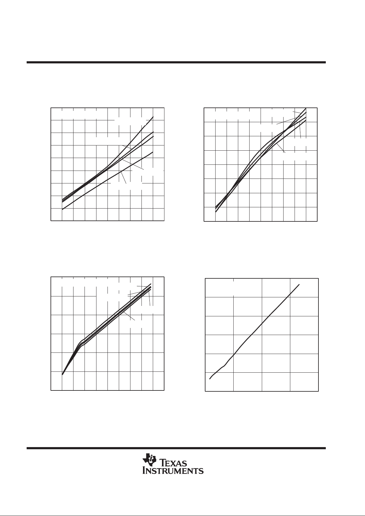
TYPICAL CHARACTERISTICS
Figure 8
49
46
45
43
45678910
– Input Current –
50
51
SUPPLY CURRENT (ENABLED)
vs
VOLTAGE
52
11 12 13 14
48
47
44
I
I
Aµ
VI– Input Voltage – V
IN = 5 V to 13 V
TA = 85°C
TA = 25°C
TA = 0°C
TA = –40°C
Figure 9
12
10
9
7
45678910
13
14
15
11 12 13 14
11
8
SUPPLY CURRENT (DISABLED)
vs
VOLTAGE
VI – Input Voltage – V
TA = 85°C
TA = 25°C
TA = 0°C
TA = –40°C
IN = 5 V to 13 V
– Input Current – nA
I
I
Figure 10
16
14
12
10
2345678
– GATE Output Voltage – V
18
20
GATE VOLTAGE
vs
INPUT VOLTAGE
22
9101112
V
O
VI – Input Voltage – V
TA = 85°C
TA = 25°C
TA = 0°C
TA = –40°C
C
L(GATE)
= 1000 pF
Figure 11
C
L(GATE)
– GATE Load Capacitance – nF
9
6
3
0
03 6
– GATE Voltage Rise Time – ms
12
15
GATE VOLTAGE RISE TIME
vs
GATE LOAD CAPACITANCE
18
912
t
r
IN = 12 V
TA = 25°C
TPS2330, TPS2331
SINGLE HOT SWAP POWER CONTROLLER WITH
CIRCUIT BREAKER AND POWER-GOOD REPORTING
SLVS277A – MARCH 2000– REVISED APRIL 2000
11
POST OFFICE BOX 655303 • DALLAS, TEXAS 75265
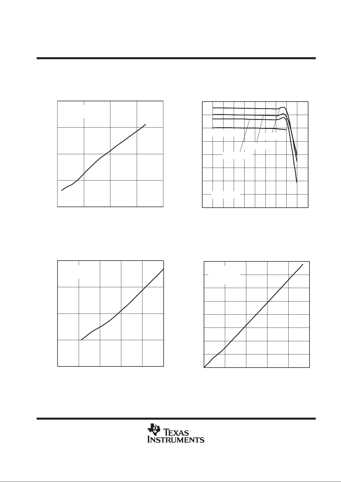
TYPICAL CHARACTERISTICS
Figure 12
1
0
036
– GATE Voltage Fall Time
2
3
GATE VOLTAGE FALL TIME
vs
GATE LOAD CAPACITANCE
4
912
t
f
C
L(GATE)
– GATE Load Capacitance – nF
IN = 12 V
TA = 25°C
Figure 13
V – GATE Voltage
13.5
13
12
11
14 15 16 17 18 19 20
I – GATE Current –
14
14.5
GATE OUTPUT CURRENT
vs
GATE VOLTAGE
15
21 22 23 24
12.5
11.5
Aµ
TA = 85°C
TA = 25°C
TA = 0°C
TA = –40°C
IN = 13 V
Figure 14
C
(timer)
– TIMER Capacitance – nF
6
3
0
0 0.2 0.4 0.6
– Circuit Braker Response Time –
9
CIRCUIT-BREAKER RESPONSE
vs
TIMER CAPACITANCE
12
0.8 1
t
res
sµ
IN = 12 V
TA = 25°C
Figure 15
CL – Load Capacitance – µF
200
160
120
0
0 100 200 300
t – Discharge Time – ms
240
280
LOAD VOLTAGE DISCHARGE TIME
vs
LOAD CAPACITANCE
320
400 500
80
40
IN = 12 V
IO = 0 A
TA = 25°C
TPS2330, TPS2331
SINGLE HOT SWAP POWER CONTROLLER WITH
CIRCUIT BREAKER AND POWER-GOOD REPORTING
SLVS277A – MARCH 2000– REVISED APRIL 2000
12
POST OFFICE BOX 655303 • DALLAS, TEXAS 75265
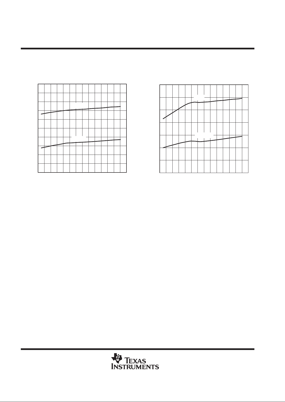
TYPICAL CHARACTERISTICS
Figure 16
TA – Temperature – °C
2.8
2.78
2.74
2.7
–45–35–25–15 –5 5 15
– Reference Voltage UVLO Threshold – V
2.84
2.88
UVLO START AND STOP THRESHOLDS
vs
TEMPERATURE
2.9
45 65 75 95
2.86
2.82
2.76
2.72
25 35 55 85
V
ref
Start
Stop
Figure 17
1.24
1.23
1.22
1.20
–45–35–25–15 –5 5 15
– Input Threshold Voltage PWRGD – V
1.25
1.26
PWRGD THRESHOLD
vs
TEMPERATURE
1.27
25 35 75 95
1.21
45 55 65 85
TA – Temperature – °C
V
IT
Up
Down

TPS2330, TPS2331
SINGLE HOT SWAP POWER CONTROLLER WITH
CIRCUIT BREAKER AND POWER-GOOD REPORTING
SLVS277A – MARCH 2000– REVISED APRIL 2000
13
POST OFFICE BOX 655303 • DALLAS, TEXAS 75265
APPLICATION INFORMATION
typical application diagram
This diagram shows a typical dual hot-swap application. The pullup resistors at PWRGD and Fault should be
relatively large (e.g. 100 kΩ) to reduce power loss unless they are required to drive a large load.
VREG
0.1 µF
IN ISET
R
ISET
ISENSE
R
SENSE
GATE
DISCH VSENSE
R
VSENSE_TOP
R
VSENSE_BOTTOM
+
FAULT
PWRGD
FAULT
PWRGD
TIMER
ENABLE
DGND
AGND
V
O
ENABLE
1 µF ∼ 10 µF
3 V ∼ 13 V IN
TPS2331
System Board
Figure 18. Typical Hot-Swap Application
input capacitor
A 0.1-µF ceramic capacitor in parallel with a 1-µF ceramic capacitor should be placed on the input power
terminals near the connector on the hot-plug board to help stabilize the voltage rails on the cards. The
TPS2330/31 does not need to be mounted near the connector or these input capacitors. For applications with
more severe power environments, a 2.2-µF or higher ceramic capacitor is recommended near the input
terminals of the hot-plug board. A bypass capacitor for IN should be placed close to the device.
output capacitor
A 0.1-µF ceramic capacitor is recommended per load on the TPS2330/31; these capacitors should be placed
close to the external FETs and to TPS2330/31. A larger bulk capacitor on the load is also recommended. The
value of the bulk capacitor should be selected based on the power requirements and the transients generated
by the application.
external FET
To deliver power from the input sources to the loads, the controller needs an external N-channel MOSFET. A
few widely used MOSFETs are shown in Table 1. But many other MOSFETs on the market can also be used
with TPS23xx in hot-swap systems.
TPS2330, TPS2331
SINGLE HOT SWAP POWER CONTROLLER WITH
CIRCUIT BREAKER AND POWER-GOOD REPORTING
SLVS277A – MARCH 2000– REVISED APRIL 2000
14
POST OFFICE BOX 655303 • DALLAS, TEXAS 75265
APPLICATION INFORMATION
Table 1. Some Available N-Channel MOSFETs
CURRENT RANGE
(A)
PART NUMBER DESCRIPTION MANUFACTURER
IRF7601 N-channel, r
DS(on)
= 0.035 Ω, 4.6 A, Micro-8 International Rectifier
MTSF3N03HDR2 N-channel, r
DS(on)
= 0.040 Ω, 4.6 A, Micro-8 ON Semiconductor
0 to 2
IRF7101 Dual N-channel, r
DS(on)
= 0.1 Ω, 2.3 A, SO-8 International Rectifier
MMSF5N02HDR2 Dual N-channel, r
DS(on)
= 0.04 Ω, 5 A, SO-8 ON Semiconductor
IRF7401 N-channel, r
DS(on)
= 0.022 Ω, 7 A, SO-8 International Rectifier
MMSF5N02HDR2 N-channel, r
DS(on)
= 0.025 Ω, 5 A, SO-8 ON Semiconductor
2 to 5
IRF7313 Dual N-channel, r
DS(on)
= 0.029 Ω, 5.2 A, SO-8 International Rectifier
SI4410 N-channel, r
DS(on)
= 0.020 Ω, 8 A, SO-8 Vishay Dale
IRLR3103 N-channel, r
DS(on)
= 0.019 Ω, 29 A, d-Pak International Rectifier
5 to 10
IRLR2703 N-channel, r
DS(on)
= 0.045 Ω, 14 A, d-Pak International Rectifier
timer
For most applications, a minimum capacitance of 50 pF is recommended to prevent false triggering. This
capacitor should be connected between TIMER and ground. The presence of an overcurrent condition on of
the TPS2330/31 causes a 50-µA current source to begin charging this capacitor. If the overcurrent condition
persists until the capacitor has been charged to approximately 0.5 V , the TPS2330/31 will latch off the transistor
and will pull the FAULT pin low. The timer capacitor can be made as large as desired to provide additional time
delay before registering a fault condition.
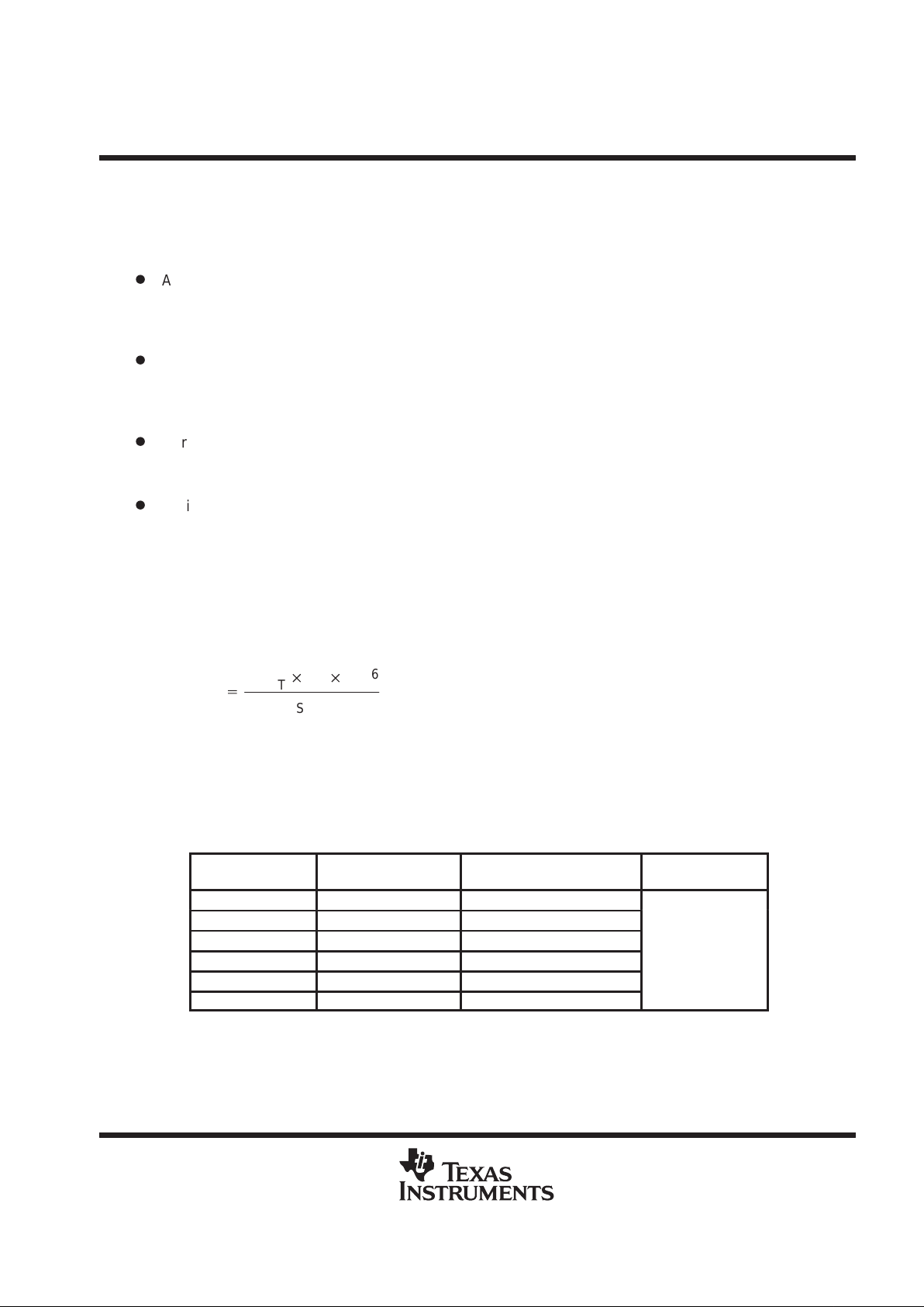
output-voltage slew-rate control
When enabled, the TPS2330/TPS2331 controllers supply the gate of an external MOSFET transistor with a
current of approximately 15 µA. The slew rate of the MOSFET source voltage is thus limited by the gate-to-drain
capacitance Cgd of the external MOSFET capacitor to a value approximating:
dvs
dt
+
15mA
C
gd
If a slower slew rate is desired, an additional capacitance can be connected between the gate of the external
MOSFET and ground.
VREG capacitor
The internal voltage regulator connected to VREG requires an external capacitor to ensure stability . A 0.1-µF
or 0.22-µF ceramic capacitor is recommended.
TPS2330, TPS2331
SINGLE HOT SWAP POWER CONTROLLER WITH
CIRCUIT BREAKER AND POWER-GOOD REPORTING
SLVS277A – MARCH 2000– REVISED APRIL 2000
15
POST OFFICE BOX 655303 • DALLAS, TEXAS 75265
APPLICATION INFORMATION
gate drive circuitry
The TPS2330/TPS2331 includes four separate features associated with each gate-drive terminal:
D
A charging current of approximately 15 µA is applied to enable the external MOSFET transistor. This current
is generated by an internal charge pump that can develop a gate-to-source potential (referenced to DISCH)
of 9 V–12 V . DISCH must be connected to the external MOSFET source terminal to ensure proper operation
of this circuitry.
D
A discharge current of approximately 75 µA is applied to disable the external MOSFET transistor. Once the
transistor gate voltage has dropped below approximately 1.5 V, this current is disabled and the UVLO
discharge driver is enabled instead. This feature allows the part to enter a low-current shutdown mode while
ensuring that the gate of the external MOSFET transistor remain at a low voltage.
D
During a UVLO condition, the gate of the MOSFET transistor is pulled down by an internal PMOS transistor.
This transistor continues to operate even if the voltage at IN is 0 V . This circuitry also helps hold the external
MOSFET transistor off when power is suddenly applied to the system.
D
During an overcurrent fault condition, the external MOSFET transistor that exhibited an over-current
condition will be rapidly turned off by an internal pulldown circuit capable of pulling in excess of 400 mA (at
4 V) from the pin. Once the gate has been pulled below approximately 1.5 V , this driver is disengaged and
the UVLO driver is enabled instead.
setting the current-limit circuit-breaker threshold
The current sensing resistor R
ISENSE
and the current limit setting resistor R
ISET
determine the current limit of
the channel, and can be calculated by the following equation:
I
LMT
+
R
ISET
50
10
–6
R
ISENSE
Typically R
ISENSE
is usually very small (0.001 Ω to 0.1 Ω). If the trace and solder-junction resistances between
the junction of R
ISENSE
and ISENSE and the junction of R
ISENSE
and R
ISET
are greater than 10% of the R
ISENSE
value, then these resistance values should be added to the R
ISENSE
value used in the calculation above.
Table 2 shows some of the current sense resistors available in the market.
T able 2. Some Current Sense Resistors
CURRENT RANGE
(A)
PART NUMBER DESCRIPTION MANUFACTURER
0 to 1 WSL-1206, 0.05 1% 0.05 Ω, 0.25 W, 1% resistor
1 to 2 WSL-1206, 0.025 1% 0.025 Ω, 0.25 W, 1% resistor
2 to 4 WSL-1206, 0.015 1% 0.015 Ω, 0.25 W, 1% resistor
4 to 6 WSL-2010, 0.010 1% 0.010 Ω, 0.5 W, 1% resistor
Vishay Dale
6 to 8 WSL-2010, 0.007 1% 0.007 Ω, 0.5 W, 1% resistor
8 to 10 WSR-2, 0.005 1% 0.005 Ω, 0.5 W, 1% resistor

TPS2330, TPS2331
SINGLE HOT SWAP POWER CONTROLLER WITH
CIRCUIT BREAKER AND POWER-GOOD REPORTING
SLVS277A – MARCH 2000– REVISED APRIL 2000
16
POST OFFICE BOX 655303 • DALLAS, TEXAS 75265
APPLICATION INFORMATION
setting the power-good threshold voltage
The two feedback resistors R
VSENSE_TOP
and R
VSENSE_BOT
connected between VO and ground form a
resistor divider setting the voltage at the VSENSE pins. VSENSE voltage equals to
V
I(SENSE)
= VO × R
VSENSE_BOT
/(R
VSENSE_TOP
+ R
VSENSE_BOT
)
This voltage is compared to an internal voltage reference (1.225 V ±2%) to determine whether the output voltage
level is within a specified tolerance. For example, given a nominal output voltage at V
O
, and defining V
O_min
as the minimum required output voltage, then the feedback resistors are defined by:
R
VSENSE_TOP
+
V
O_min
*
1.225
1.225
R
VSENSE_BOT
Start the process by selecting a large standard resistor value for R
VSENSE_BOT
to reduce power loss. Then
R
VSENSE_TOP
can be calculated by inserting all of the known values into the equation above. When VO is lower
than V
O_min
, PWRGD will be low as long as the controller is enabled.
undervoltage lockout (UVLO)
The TPS2330/TPS2331 includes an undervoltage lockout (UVLO) feature that monitors the voltage present on
the VREG pin. This feature will disable the external MOSFET if the voltage on VREG drops below 2.78 V
(nominal) and will re-enable normal operation when it rises above 2.85 V (nominal). Since VREG is fed from
IN through a low-dropout voltage regulator, the voltage on VREG will track the voltage on IN within 50 mV . While
the undervoltage lockout is engaged, GA TE is held low by an internal PMOS pulldown transistor , ensuring that
the external MOSFET transistor remain off at the times, even if the power supply has fallen to 0 V.
power-up control
The TPS2330/TPS2331 includes a 500 µs (nominal) startup delay that ensures that internal circuitry has
sufficient time to start before the device begins turning on the external MOSFETs. This delay is triggered only
upon the rapid application of power to the circuit. If the power supply ramps up slowly , the undervoltage lockout
circuitry will provide adequate protection against undervoltage operation.
3-channel hot-swap application
Some applications require hot-swap control of up to three voltage rails, but may not explicitly require the sensing
of the status of the output power on all three of the voltage rails. One such application is device bay , where dv/dt
control of 3.3 V , 5 V , and 12 V is required. By using TPS2330/TPS2331 to drive all three power rails, as is shown
below, TPS2330/31 can deliver three dif ferent voltages to three loads while monitoring the status of one of the
loads.

TPS2330, TPS2331
SINGLE HOT SWAP POWER CONTROLLER WITH
CIRCUIT BREAKER AND POWER-GOOD REPORTING
SLVS277A – MARCH 2000– REVISED APRIL 2000
17
POST OFFICE BOX 655303 • DALLAS, TEXAS 75265
APPLICATION INFORMATION
V
reg
0.1 µF
IN ISET
R
ISET
ISENSE
R
SENSE
GATE
DISCH VSENSE
R
VSENSE_TOP
R
VSENSE_BOTTOM
+
FAULT
PWRGD
FAULT
PWRGD
TIMER
ENABLE
DGND
AGND
R
g1
+
V
O1
V
O2
ENABLE
1 µF ∼ 10 µF
1 µF ∼ 10 µF
12 V IN1
3.3 V IN2
TPS2331
+
V
O3
1 µF ∼ 10 µF
5 V IN3
System Board
R
g3
R
g2
Figure 19. Three-Channel Application
Figure 29 shows ramp-up waveforms of the three output voltages.
V
O1
V
O3
V
O2
– Output Voltage – 2 V/div
V
O
t – Time – 2.5 ms/div
Figure 20

TPS2330, TPS2331
SINGLE HOT SWAP POWER CONTROLLER WITH
CIRCUIT BREAKER AND POWER-GOOD REPORTING
SLVS277A – MARCH 2000– REVISED APRIL 2000
18
POST OFFICE BOX 655303 • DALLAS, TEXAS 75265
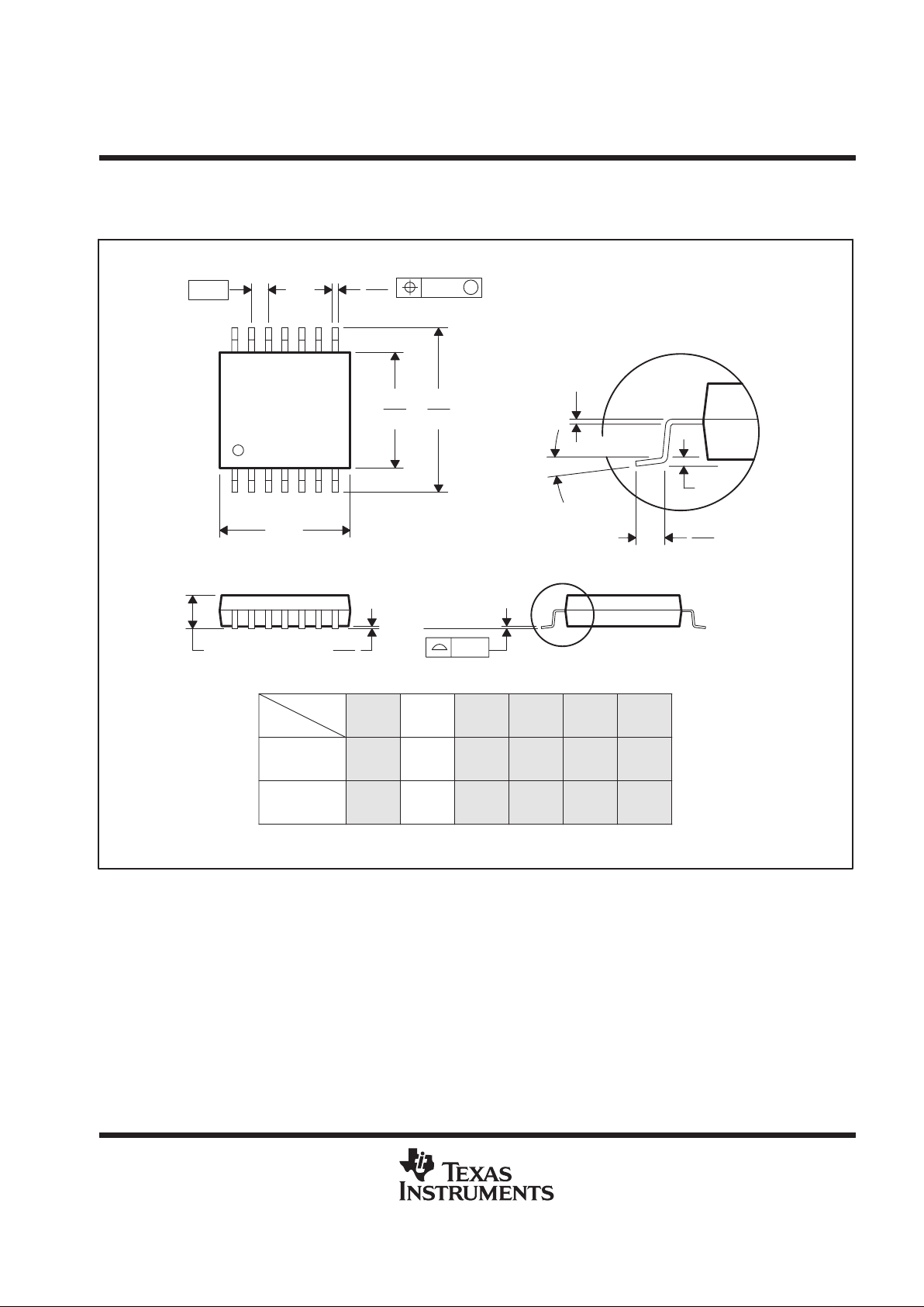
MECHANICAL DATA
D (R-PDSO-G**) PLASTIC SMALL-OUTLINE PACKAGE
14 PINS SHOWN
4040047/D 10/96
0.228 (5,80)
0.244 (6,20)
0.069 (1,75) MAX
0.010 (0,25)
0.004 (0,10)
1
14
0.014 (0,35)
0.020 (0,51)
A
0.157 (4,00)
0.150 (3,81)
7
8
0.044 (1,12)
0.016 (0,40)
Seating Plane
0.010 (0,25)
PINS **
0.008 (0,20) NOM
A MIN
A MAX
DIM
Gage Plane
0.189
(4,80)
(5,00)
0.197
8
(8,55)
(8,75)
0.337
14
0.344
(9,80)
16
0.394
(10,00)
0.386
0.004 (0,10)
M
0.010 (0,25)
0.050 (1,27)
0°–8°
NOTES: A. All linear dimensions are in inches (millimeters).
B. This drawing is subject to change without notice.
C. Body dimensions do not include mold flash or protrusion, not to exceed 0.006 (0,15).
D. Falls within JEDEC MS-012
TPS2330, TPS2331
SINGLE HOT SWAP POWER CONTROLLER WITH
CIRCUIT BREAKER AND POWER-GOOD REPORTING
SLVS277A – MARCH 2000– REVISED APRIL 2000
19
POST OFFICE BOX 655303 • DALLAS, TEXAS 75265
MECHANICAL DATA
PW (R-PDSO-G**) PLASTIC SMALL-OUTLINE PACKAGE
14 PINS SHOWN
0,65
M
0,10
0,10
0,25
0,50
0,75
0,15 NOM
Gage Plane
28
9,80
9,60
24
7,90
7,70
2016
6,60
6,40
4040064/F 01/97
0,30
6,60
6,20
8
0,19
4,30
4,50
7
0,15
14
A
1
1,20 MAX
14
5,10
4,90
8
3,10
2,90
A MAX
A MIN
DIM
PINS **
0,05
4,90
5,10
Seating Plane
0°–8°
NOTES: A. All linear dimensions are in millimeters.
B. This drawing is subject to change without notice.
C. Body dimensions do not include mold flash or protrusion not to exceed 0,15.
D. Falls within JEDEC MO-153

IMPORTANT NOTICE
T exas Instruments and its subsidiaries (TI) reserve the right to make changes to their products or to discontinue
any product or service without notice, and advise customers to obtain the latest version of relevant information
to verify, before placing orders, that information being relied on is current and complete. All products are sold
subject to the terms and conditions of sale supplied at the time of order acknowledgment, including those
pertaining to warranty, patent infringement, and limitation of liability.
TI warrants performance of its semiconductor products to the specifications applicable at the time of sale in
accordance with TI’s standard warranty. Testing and other quality control techniques are utilized to the extent
TI deems necessary to support this warranty. Specific testing of all parameters of each device is not necessarily
performed, except those mandated by government requirements.
Customers are responsible for their applications using TI components.
In order to minimize risks associated with the customer’s applications, adequate design and operating
safeguards must be provided by the customer to minimize inherent or procedural hazards.
TI assumes no liability for applications assistance or customer product design. TI does not warrant or represent
that any license, either express or implied, is granted under any patent right, copyright, mask work right, or other
intellectual property right of TI covering or relating to any combination, machine, or process in which such
semiconductor products or services might be or are used. TI’s publication of information regarding any third
party’s products or services does not constitute TI’s approval, warranty or endorsement thereof.
Copyright 2000, Texas Instruments Incorporated
 Loading...