Texas Instruments TPS2321IPWR, TPS2321IPW, TPS2321IDR, TPS2321ID, TPS2320IPWR Datasheet
...
TPS2320, TPS2321
DUAL HOT SWAP POWER CONTROLLER
WITH INDEPENDENT CIRCUIT BREAKER
SLVS276A – MARCH 200 – REVISED APRIL 2000
1
POST OFFICE BOX 655303 • DALLAS, TEXAS 75265
features
D
Dual-Channel High-Side MOSFET Drivers
D
IN1: 3 V to 13 V; IN2: 3 V to 5.5 V
D
Inrush Current Limiting With dv/dt Control
D
Independent Circuit-Breaker Control With
Programmable Current Limit and Transient
Timer
D
CMOS- and TTL-Compatible Enable Input
D
Low, 5-µA Standby Supply Current ...Max
D
Available in 16-Pin SOIC and TSSOP
Package
D
–40°C to 85°C Ambient Temperature Range
D
Electrostatic Discharge Protection
applications
D
Hot-Swap/Plug/Dock Power Management
D
Hot-Plug PCI, Device Bay
D
Electronic Circuit Breaker
description
The TPS2320 and TPS2321 are dual-channel
hot-swap controllers that use external N-channel
MOSFETs as high-side switches in power
applications. Features of these devices, such as
overcurrent protection (OCP), inrush-current
control, and separation of load transients from
actual load increases, are critical requirements for
hot-swap applications.
The TPS2320/21 devices incorporate undervoltage lockout (UVLO) to ensure the device is off at startup. Each
internal charge pump, capable of driving multiple MOSFETs, provides enough gate-drive voltage to fully
enhance the N-channel MOSFETs. The charge pumps control both the rise times and fall times (dv/dt) of the
MOSFETs, reducing power transients during power up/down. The circuit-breaker functionality combines the
ability to sense overcurrent conditions with a timer function; this allows designs such as DSPs, that may have
high peak currents during power-state transitions, to disregard transients for a programmable period.
AVAILABLE OPTIONS
PIN
PACKAGES
TAHOT-SWAP CONTROLLER DESCRIPTION
COUNT
ENABLE ENABLE
Dual-channel with independent OCP and adjustable PG 20 TPS2300IPW TPS2301IPW
Dual-channel with interdependent OCP and adjustable PG 20 TPS2310IPW TPS2311IPW
–40°C to 85°C
Dual-channel with independent OCP 16
TPS2320ID
TPS2320IPW
TPS2321ID
TPS2321IPW
Single-channel with OCP and adjustable PG 14
TPS2330ID
TPS2330IPW
TPS2331ID
TPS2331IPW
†
The packages are available left-end taped and reeled (indicated by the R suffix on the device type; e.g., TPS2321IPWR).
Copyright 2000, Texas Instruments Incorporated
PRODUCTION DATA information is current as of publication date.
Products conform to specifications per the terms of Texas Instruments
standard warranty. Production processing does not necessarily include
testing of all parameters.
Please be aware that an important notice concerning availability, standard warranty, and use in critical applications of
Texas Instruments semiconductor products and disclaimers thereto appears at the end of this data sheet.
typical application
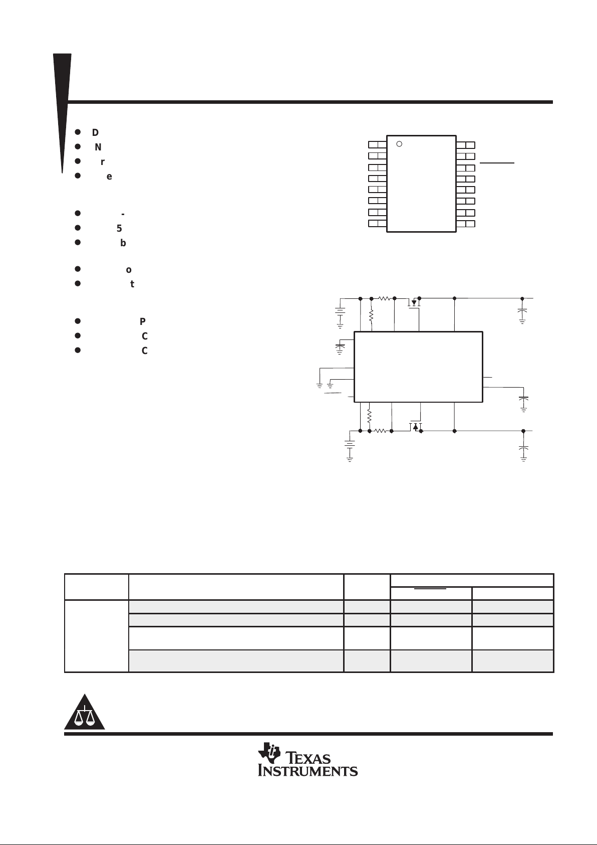
NOTE: Terminal 14 is active high on TPS2321.
VREG
IN1
ISET1
ISENSE1
GATE1
DISCH1
FAULT
TIMER
DISCH2
GATE2
ISENSE2ISET2IN2
ENABLE
DGND
AGND
V2
V1
3 V – 5.5 V
3 V – 13 V
TPS2320
+
V
O1
V
O2
+
1
2
3
4
5
6
7
8
16
15
14
13
12
11
10
9
GATE1
GATE2
DGND
TIMER
VREG
AGND
ISENSE2
ISENSE1
DISCH1
DISCH2
ENABLE
FAULT
ISET1
ISET2
IN2
IN1
D OR PW PACKAGE
(TOP VIEW)
TPS2320, TPS2321
DUAL HOT SWAP POWER CONTROLLER
WITH INDEPENDENT CIRCUIT BREAKER
SLVS276A – MARCH 200 – REVISED APRIL 2000
2
POST OFFICE BOX 655303 • DALLAS, TEXAS 75265
functional block diagram
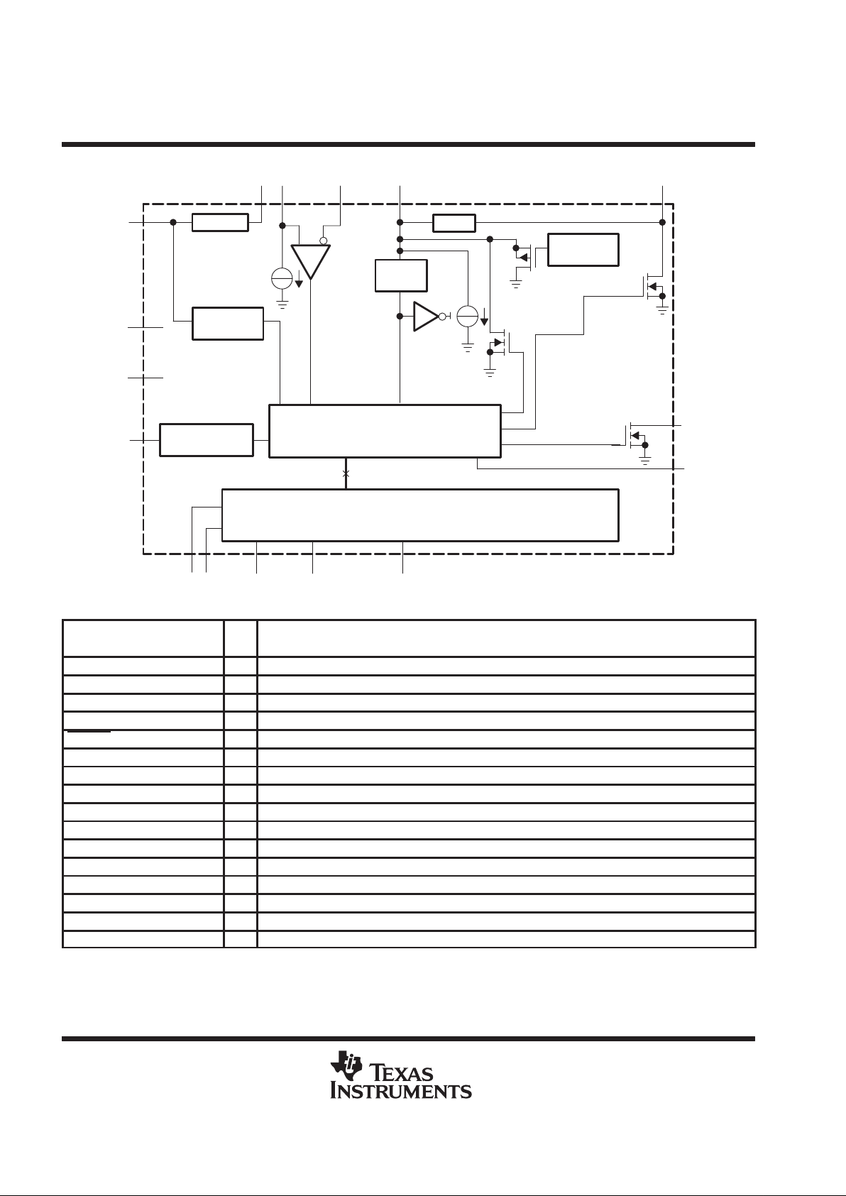
PREREG
UVLO and
Power-Up
IN1 ISET1 ISENSE1 GATE1
Clamp
Charge
Pump
75 µA
Pulldown FET
Circuit Breaker
dv/dt Rate
Protection
DISCH1
Logic
FAULT
TIMER
Second Channel
GATE2ISENSE2ISET2IN2
DISCH2
Circuit
Breaker
VREG
50-µs Deglitch
AGND
DGND
ENABLE
50 µA
Terminal Functions
TERMINAL
NAME NO.
I/O
DESCRIPTION
AGND 6 I Analog ground, connects to DGND as close as possible
DGND 3 I Digital ground
DISCH1 16 O Discharge transistor 1
DISCH2 15 O Discharge transistor 2
ENABLE/ ENABLE 14 I Active low (TPS2320) or active high enable (TPS2321)
FAULT 13 O Overcurrent fault, open-drain output
GATE1 1 O Connects to gate of channel 1 high-side MOSFET
GATE2 2 O Connects to gate of channel 2 high-side MOSFET
IN1 9 I Input voltage for channel 1
IN2 10 I Input voltage for channel 2
ISENSE1 8 I Current-sense input channel 1
ISENSE2 7 I Current-sense input channel 2
ISET1 12 I Adjusts circuit-breaker threshold with resistor connected to IN1
ISET2 11 I Adjusts circuit-breaker threshold with resistor connected to IN2
TIMER 4 O Adjusts circuit-breaker deglitch time
VREG 5 O Connects to bypass capacitor, for stable operation

TPS2320, TPS2321
DUAL HOT SWAP POWER CONTROLLER
WITH INDEPENDENT CIRCUIT BREAKER
SLVS276A – MARCH 200 – REVISED APRIL 2000
3
POST OFFICE BOX 655303 • DALLAS, TEXAS 75265
detailed description
DISCH1, DISCH2 – DISCH1 and DISCH2 should be connected to the sources of the external N-channel
MOSFET transistors connected to GA TE1 and GA TE2, respectively. These pins discharge the loads when the
MOSFET transistors are disabled. They also serve as reference-voltage connections for internal gate
voltage-clamp circuitry.
ENABLE
or ENABLE – ENABLE for TPS2320 is active low. ENABLE for TPS2321 is active high. When the
controller is enabled, both GA TE1 and GATE2 voltages will power up to turn on the external MOSFETs. When
the ENABLE pin is pulled high for TPS2320 or the ENABLE pin is pulled low for TPS2321 for more than 50 µs,
the gate of the MOSFET is discharged at a controlled rate by a current source, and a transistor is enabled to
discharge the output bulk capacitance. In addition, the device turns on the internal regulator PREREG (see
VREG) when enabled and shuts down PREREG when disabled so that total supply current is much less than
5 µA.
FAULT – FAULT is an open-drain overcurrent flag output. When an overcurrent condition in either channel is
sustained long enough to charge TIMER to 0.5 V , the overcurrent channel latches off and pulls F AUL T low . The
other channel will run normally if not in overcurrent.
GA TE1, GA TE2 – GATE1 and GATE2 connect to the gates of external N-channel MOSFET transistors. When
the device is enabled, internal charge-pump circuitry pulls these pins up by sourcing approximately 15 µA to
each. The turnon slew rates depend upon the capacitance present at the GATE1 and GATE2 terminals. If
desired, the turnon slew rates can be further reduced by connecting capacitors between these pins and ground.
These capacitors also reduce inrush current and protect the device from false overcurrent triggering during
powerup. The charge-pump circuitry will generate gate-to-source voltages of 9 V–12 V across the external
MOSFET transistors.
IN1, IN2 – IN1 and IN2 should be connected to the power sources driving the external N-channel MOSFET
transistors connected to GA TE1 and GA TE2, respectively . The TPS2320/TPS2321 draws its operating current
from IN1, and both channels will remain disabled until the IN1 power supply has been established. The IN1
channel has been constructed to support 3-V, 5-V, or 12-V operation, while the IN2 channel has been
constructed to support 3-V or 5-V operation
ISENSE1, ISENSE2, ISET1, ISET2 – ISENSE1 and ISENSE2, in combination with ISET1 and ISET2,
implement overcurrent sensing for GA TE1 and GA TE2. ISET1 and ISET2 set the magnitude of the current that
generates an overcurrent fault, through external resistors connected to ISET1 and ISET2. An internal current
source draws 50 µA from ISET1 and ISET2. With a sense resistor from IN1 to ISENSE1 or from IN2 to ISENSE2,
which is also connected to the drains of external MOSFETs, the voltage on the sense resistor reflects the load
current. An overcurrent condition is assumed to exist if ISENSE1 is pulled below ISET1 or if ISENSE2 is pulled
below ISET2.
TIMER – A capacitor on TIMER sets the time during which the power switch can be in overcurrent before turning
off. When the overcurrent protection circuits sense an excessive current, a current source is enabled which
charges the capacitor on TIMER. Once the voltage on TIMER reaches approximately 0.5 V , the circuit-breaker
latch is set and the power switch is latched off. Power must be recycled or the ENABLE pin must be toggled
to restart the controller. In high-power or high-temperature applications, a minimum 50-pF capacitor is strongly
recommended from TIMER to ground, to prevent any false triggering.
VREG – The VREG pin is the output of an internal low-dropout voltage regulator. This regulator draws current
from IN1. A 0.1-µF ceramic capacitor should be connected between VREG and ground. VREG can be
connected to IN1, IN2, or to a separated power supply through a low-resistance resistor. However , the voltage
on VREG must be less than 5.5 V.
TPS2320, TPS2321
DUAL HOT SWAP POWER CONTROLLER
WITH INDEPENDENT CIRCUIT BREAKER
SLVS276A – MARCH 200 – REVISED APRIL 2000
4
POST OFFICE BOX 655303 • DALLAS, TEXAS 75265
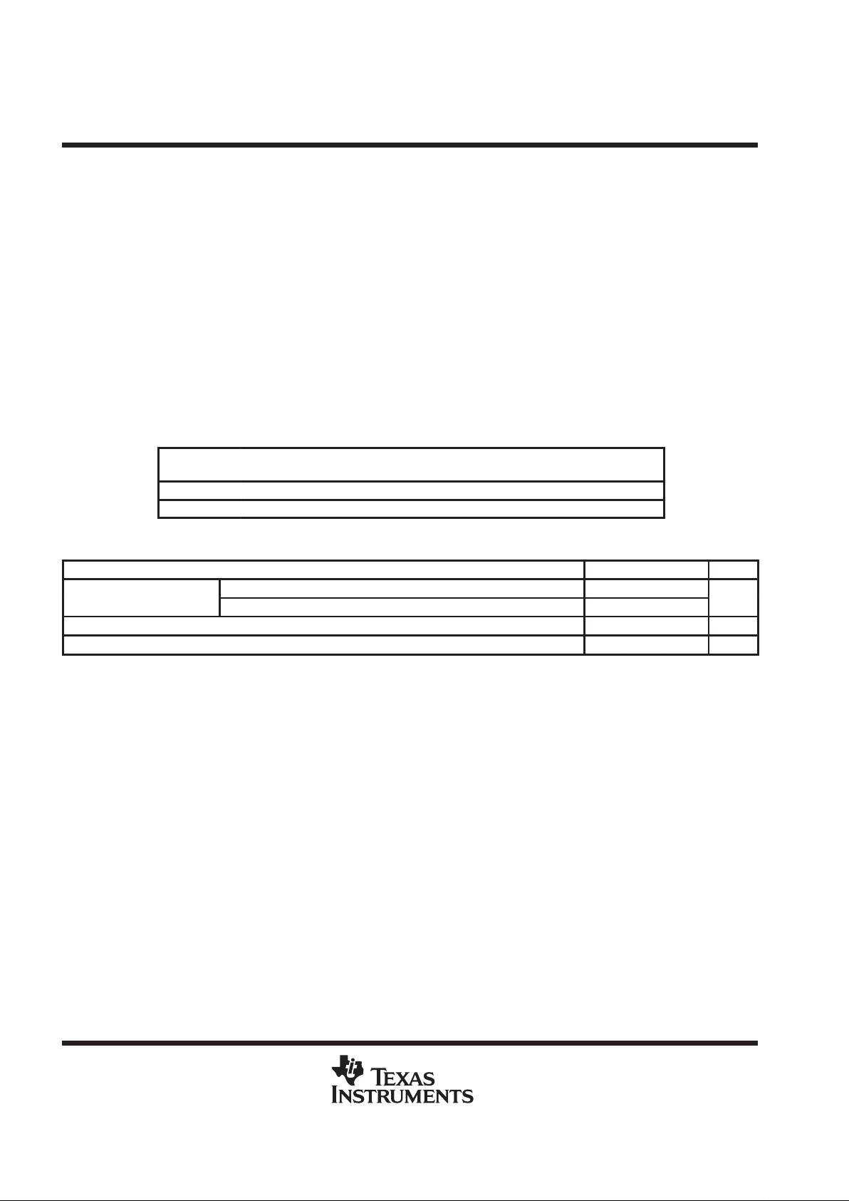
absolute maximum ratings over operating free-air temperature (unless otherwise noted)
†
Input voltage range: V
I(IN1)
, V
I(ISENSE1)
, V
I(ISET1)
, V
I(ENABLE)
–0.3 V to 15 V. . . . . . . . . . . . . . . . . . . . . . .
V
I(IN2)
, V
I(ISENSE2)
, V
I(ISET2)
–0.3 V to 7 V. . . . . . . . . . . . . . . . . . . . . . . . . . . . . . . . . . . .
Output voltage range: V
O(GATE1)
–0.3 V to 30 V. . . . . . . . . . . . . . . . . . . . . . . . . . . . . . . . . . . . . . . . . . . . . . . . .
V
O(GATE2)
–0.3 V to 22V. . . . . . . . . . . . . . . . . . . . . . . . . . . . . . . . . . . . . . . . . . . . . . . . . .
V
O(DISCH1)
, V
O(FAULT)
, V
O(VREG)
, V
O(DISCH2)
, V
O(TIMER)
, –0.3 V to 15V. . . . .
Sink current range: I
GATE1
, I
GATE2
, I
DISCH1
, I
DISCH2
0 mA to 100 mA. . . . . . . . . . . . . . . . . . . . . . . . . . . . . .
I
TIMER
, I
FAUL T
0 mA to 10 mA. . . . . . . . . . . . . . . . . . . . . . . . . . . . . . . . . . . . . . . . . . . . . . . .
Operating virtual junction temperature range, TJ –40°C to 100°C. . . . . . . . . . . . . . . . . . . . . . . . . . . . . . . . . . . . .
Storage temperature range, T
stg
–55°C to 150°C. . . . . . . . . . . . . . . . . . . . . . . . . . . . . . . . . . . . . . . . . . . . . . . . . . .
Lead temperature 1,6 mm (1/16 inch) from case for 10 seconds 260°C. . . . . . . . . . . . . . . . . . . . . . . . . . . . . . .
†
Stresses beyond those listed under “absolute maximum ratings” may cause permanent damage to the device. These are stress ratings only, and
functional operation of the device at these or any other conditions beyond those indicated under “recommended operating conditions” is not
implied. Exposure to absolute-maximum-rated conditions for extended periods may affect device reliability.
NOTE 1: All voltages are respect to DGND.
DISSIPATION RATING TABLE
PACKAGE
TA ≤ 25°C
POWER RATING
DERATING FACTOR
ABOVE TA = 25°C
TA = 70°C
POWER RATING
TA = 85°C
POWER RATING
PW-16 823 mW 10.98 mW/°C 329 mW 165 mW
D-16 674 mW 8.98 mW/°C 270 mW 135 mW
recommended operating conditions
MIN NOM MAX UNIT
p
V
I(IN1)
, V
I(ISENSE1)
, V
I(ISET1)
3 13
Input voltage, V
I
V
I(IN2)
, V
I(ISENSE2)
, V
I(ISET2)
3 5.5
V
VREG voltage, V
O(VREG)
, when VREG is directly connected to IN1 2.95 5.5 V
Operating virtual junction temperature, T
J
–40 100 °C
TPS2320, TPS2321
DUAL HOT SWAP POWER CONTROLLER
WITH INDEPENDENT CIRCUIT BREAKER
SLVS276A – MARCH 200 – REVISED APRIL 2000
5
POST OFFICE BOX 655303 • DALLAS, TEXAS 75265
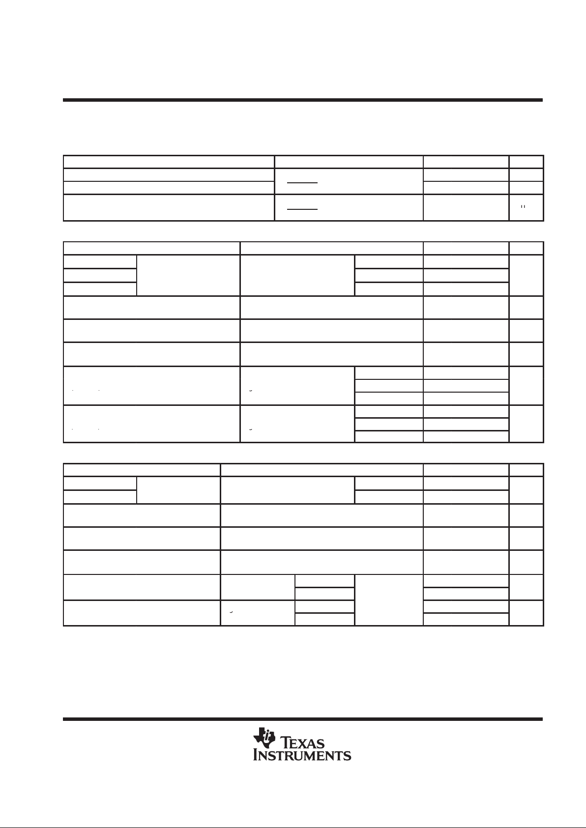
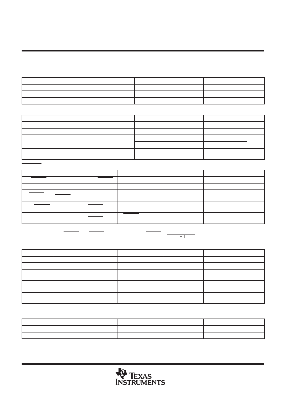
electrical characteristics over recommended operating temperature range (–40°C < TA < 85°C),
3 V ≤ V
I(IN1)
≤13 V, 3 V ≤ V
I(IN2)
≤ 5.5 V (unless otherwise noted)
general
PARAMETER TEST CONDITIONS MIN TYP MAX UNIT
I
I(IN1)
Input current, IN1 V
I(ENABLE)
= 5 V (TPS2321), 0.5 1 mA
I
I(IN2)
Input current, IN2 V
I(ENABLE)
= 0 V (TPS2320) 75 200 µA
Standby current (sum of currents into IN1, IN2,
V
I(ENABLE)
= 0 V (TPS2321),
I
I(stby)
y(
ISENSE1, ISENSE2, ISET1, and ISET2)
V
I(ENABLE)
= 5 V (TPS2320)
5
µA
GATE1
PARAMETER TEST CONDITIONS MIN TYP MAX UNIT
V
G(GATE1_3V)
V
I(IN1)
= 3 V 9 11.5
V
G(GATE1_4.5V)
Gate voltage
I
I(GATE1)
=
500 nA
,
DISCH1 open
V
I(IN1)
= 4.5 V 10.5 14.5
V
V
G(GATE1_10.8V)
DISCH1 oen
V
I(IN1)
= 10.8 V 16.8 21
V
C(GATE1)
Clamping voltage, GATE1
to DISCH1
9 10 12 V
I
S(GATE1)
Source current, GATE1
3 V ≤ V
I(IN1)
≤ 13.2 V, 3 V ≤ V
O(VREG)
≤ 5.5 V,
V
I(GATE1)
= V
I(IN1)
+ 6 V
10 14 20 µA
Sink current, GATE1
3 V ≤ V
I(IN1)
≤ 13.2 V, 3 V ≤ V
O(VREG)
≤ 5.5 V,
V
I(GATE1)
= V
I(IN1)
50 75 100 µA
V
I(IN1)
= 3 V 0.5
t
r(GATE1)
Rise time, GATE1 Cg to GND = 1 nF (see Note 2)
V
I(IN1)
= 4.5 V 0.6
ms
()
g
V
I(IN1)
= 10.8 V 1
V
I(IN1)
= 3 V 0.1
t
f(GATE1)
Fall time, GATE1 Cg to GND = 1 nF (see Note 2)
V
I(IN1)
= 4.5 V 0.12
ms
()
g
V
I(IN1)
= 10.8 V 0.2
GATE2
PARAMETER TEST CONDITIONS MIN TYP MAX UNIT
V
G(GATE2_3V)
p
V
I(IN2)
= 3 V 9 11.7
V
G(GATE2_4.5V)
Gate voltage
I
I(GATE2)
=
500 nA, DISCH2 oen
V
I(IN2)
= 4.5 V 10.5 14.7
V
V
C(GATE2)
Clamping voltage,
GATE2 to DISCH2
9 10 12 V
I
S(GATE2)
Source current,
GATE2
3 V ≤ V
I(IN2)
≤ 5.5 V, 3 V ≤ V
O(VREG)
≤ 5.5 V,
V
I(GATE2)
= V
I(IN2)
+ 6 V
10 14 20 µA
Sink current, GATE2
3 V ≤ V
I(IN2)
≤ 5.5 V, 3 V ≤ V
O(VREG)
≤ 5.5 V,
V
I(GATE2)
= V
I(IN2)
50 75 100 µA
C
to GND = 1 nF
V
I(IN2)
= 3 V 0.5
t
r(GATE2)
Rise time, GATE2
g
(see Note 2)
V
I(IN2)
= 4.5 V
0.6
ms
Cg to GND = 1 nF
V
I(IN2)
= 3 V
V
O(VREG)
= 3
V
0.1
t
f(GATE2)
Fall time, GATE2
g
(see Note 2)
V
I(IN2)
= 4.5 V 0.12
ms
NOTE 2: Specified, but not production tested.
TPS2320, TPS2321
DUAL HOT SWAP POWER CONTROLLER
WITH INDEPENDENT CIRCUIT BREAKER
SLVS276A – MARCH 200 – REVISED APRIL 2000
6
POST OFFICE BOX 655303 • DALLAS, TEXAS 75265
electrical characteristics over recommended operating temperature range (–40°C < TA < 85°C),
3 V ≤ V
I(IN1)
≤13 V, 3 V ≤ V
I(IN2)
≤ 5.5 V ( unless otherwise noted) (continued)
TIMER
PARAMETER TEST CONDITIONS MIN TYP MAX UNIT
V
OT(TIMER)
Threshold voltage, TIMER 0.4 0.5 0.6 V
Charge current, TIMER V
I(TIMER)
= 0 V 35 50 65 µA
Discharge current, TIMER V
I(TIMER)
= 1 V 1 2.5 mA
circuit breaker
PARAMETER TEST CONDITIONS MIN TYP MAX UNIT
V
IT(CB)
Undervoltage voltage, circuit breaker R
ISETx
= 1 kΩ 40 50 60 mV
I
IB(ISENSEx)
Input bias current, I
SENSEx
0.1 5 µA
V
O(GATEx)
= 4 V 400 800
Discharge current, GATE
x
V
O(GATEx)
= 1 V
25 150
mA
t
pd(CB)
Propagation (delay) time, comparator inputs to
gate output
Cg = 50 pF,
(50% to 10%)
10 mV overdrive,
C
O(timer)
= 50 pF
1.3 µs
ENABLE, active low (TPS2320)
PARAMETER TEST CONDITIONS MIN TYP MAX UNIT
V
IH(ENABLE)
High-level input voltage, ENABLE 2 V
V
IL(ENABLE
)
Low-level input voltage, ENABLE 0.8 V
R
I(ENABLE
)
Input pullup resistance,
ENABLE
See Note 3 100 200 300 kΩ
t
d_off(ENABLE)
Turnoff delay time, ENABLE
V
I(ENABLE)
increasing above stop threshold; 100
ns rise time, 20 mV overdrive (see Note 2)
60 µs
t
d_on(ENABLE)
Turnon delay time, ENABLE
V
I(ENABLE
)
decreasing below start threshold;
100 ns fall time, 20 mV overdrive (see Note 2)
125 µs
NOTES: 2. Specified, but not production tested.
3. Test IO of ENABLE
at V
I(ENABLE
)
= 1 V and 0 V, then R
I(ENABLE)
=
1V
I
O_
0V
*
I
O_
1V
ENABLE, active high (TPS2321)
PARAMETER TEST CONDITIONS MIN TYP MAX UNIT
V
IH(ENABLE)
High-level input voltage, ENABLE 2 V
V
IL(ENABLE)
Low-level input voltage, ENABLE 0.7 V
R
I(ENABLE)
Input pulldown resistance,
ENABLE
100 150 300 kΩ
t
d_on(ENABLE)
Turnon delay time, ENABLE
V
I(ENABLE)
increasing above start threshold;
100 ns rise time, 20 mV overdrive (see Note 2)
85 µs
t
d_off(ENABLE)
Turnoff delay time, ENABLE
V
I(ENABLE)
decreasing below stop threshold;
100 ns fall time, 20 mV overdrive (see Note 2)
100 µs
NOTE 2: Specified, but not production tested.
PREREG
PARAMETER TEST CONDITIONS MIN TYP MAX UNIT
VREG PREREG output voltage 4.5 ≤ V
I(IN1)
≤ 13 V 3.5 4.1 5.5 V
Vdrop_PREREG PREREG dropout voltage V
I(IN1)
= 3 V 0.1 V
TPS2320, TPS2321
DUAL HOT SWAP POWER CONTROLLER
WITH INDEPENDENT CIRCUIT BREAKER
SLVS276A – MARCH 200 – REVISED APRIL 2000
7
POST OFFICE BOX 655303 • DALLAS, TEXAS 75265
electrical characteristics over recommended operating temperature range (–40°C < TA < 85°C),
3 V ≤ V
I(IN1)
≤13 V, 3 V ≤ V
I(IN2)
≤ 5.5 V (unless otherwise noted) (continued)
VREG UVLO
PARAMETER TEST CONDITIONS MIN TYP MAX UNIT
V
OT(UVLOstart)
Output threshold voltage, start 2.75 2.85 2.95 V
V
OT(UVLOstop)
Output threshold voltage, stop 2.65 2.78 V
V
hys(UVLO)
Hysteresis 50 75 mV
UVLO sink current, GATEx V
I(GATEx)
= 2 V 10 mA
FAULT output
PARAMETER TEST CONDITIONS MIN TYP MAX UNIT
V
O(sat)(FAULT)
Output saturation voltage, FAULT IO = 2 mA 0.4 V
I
lkg(FAULT)
Leakage current, FAULT V
O(FAULT)
= 13 V 1 µA
DISCH1 and DISCH2
PARAMETER TEST CONDITIONS MIN TYP MAX UNIT
I
DISCH
Discharge current, DISCHx V
I(DISCHx)
= 1.5 V, V
I(VIN1)
= 5 V 5 10 mA
V
IH(DISCH)
Discharge on high-level input voltage 2 V
V
IL(DISCH)
Discharge on low-level input voltage 1 V
 Loading...