

Page 1

TMS320DM646x DMSoC
Asynchronous External Memory Interface
(EMIF)
User's Guide
Literature Number: SPRUEQ7C
February 2010
Page 2

2
SPRUEQ7C–February 2010
Submit Documentation Feedback
Copyright © 2010, Texas Instruments Incorporated
Page 3

Preface ....................................................................................................................................... 6
1 Introduction ........................................................................................................................ 8
1.1 Purpose of the Peripheral .............................................................................................. 8
1.2 Features .................................................................................................................. 8
1.3 Functional Block Diagram .............................................................................................. 9
2 Architecture ........................................................................................................................ 9
2.1 Clock Control ............................................................................................................. 9
2.2 EMIF Requests .......................................................................................................... 9
2.3 Signal Descriptions .................................................................................................... 10
2.4 Pin Multiplexing ........................................................................................................ 10
2.5 Asynchronous Controller and Interface ............................................................................. 10
3 Use Cases ........................................................................................................................ 30
3.1 Interfacing to Asynchronous SRAM (ASRAM) ..................................................................... 30
3.2 Interfacing to NAND Flash ............................................................................................ 39
4 Registers .......................................................................................................................... 48
4.1 Revision Code and Status Register (RCSR) ....................................................................... 49
4.2 Asynchronous Wait Cycle Configuration Register (AWCCR) .................................................... 50
4.3 Asynchronous n Configuration Registers (A1CR-A4CR) ......................................................... 52
4.4 EMIF Interrupt Raw Register (EIRR) ................................................................................ 53
4.5 EMIF Interrupt Mask Register (EIMR) ............................................................................... 54
4.6 EMIF Interrupt Mask Set Register (EIMSR) ........................................................................ 56
4.7 EMIF Interrupt Mask Clear Register (EIMCR) ..................................................................... 58
4.8 NAND Flash Control Register (NANDFCR) ........................................................................ 60
4.9 NAND Flash Status Register (NANDFSR) ......................................................................... 61
4.10 NAND Flash n ECC Registers (NANDF1ECC-NANDF4ECC) ................................................... 61
Appendix A Revision History ...................................................................................................... 63
SPRUEQ7C–February 2010 Table of Contents
Submit Documentation Feedback
Copyright © 2010, Texas Instruments Incorporated
3
Page 4

www.ti.com
List of Figures
1 EMIF Functional Block Diagram .......................................................................................... 9
2 EMIF Asynchronous Interface ........................................................................................... 11
3 EMIF to 8-bit and 16-bit Memory Interfaces ........................................................................... 11
4 Timing Waveform of an Asynchronous Read Cycle in Normal Mode .............................................. 15
5 Timing Waveform of an Asynchronous Write Cycle in Normal Mode .............................................. 17
6 Timing Waveform of an Asynchronous Read Cycle in Select Strobe Mode....................................... 19
7 Timing Waveform of an Asynchronous Write Cycle in Select Strobe Mode....................................... 21
8 EMIF to NAND Flash Interface .......................................................................................... 23
9 ECC Value for 8-Bit NAND Flash ....................................................................................... 25
10 EMIF to 16-Bit Multiplexed HPI16 Interface............................................................................ 26
11 Connecting the EMIF to the TC55V16100FT-12...................................................................... 30
12 Timing Waveform of an ASRAM Read ................................................................................ 32
13 Timing Waveform of an ASRAM Write ................................................................................. 33
14 Timing Waveform of an ASRAM Read with PCB Delays ............................................................ 35
15 Timing Waveform of an ASRAM Write with PCB Delays ............................................................ 36
16 Timing Waveform of a NAND Flash Read ............................................................................ 41
17 Timing Waveform of a NAND Flash Command Write ............................................................... 43
18 Timing Waveform of a NAND Flash Address Write .................................................................. 43
19 Timing Waveform of a NAND Flash Data Write ...................................................................... 44
20 Revision Code and Status Register (RCSR) .......................................................................... 49
21 Asynchronous Wait Cycle Configuration Register (AWCCR)........................................................ 50
22 Asynchronous n Configuration Register (ACFGn) .................................................................... 52
23 EMIF Interrupt Raw Register (EIRR).................................................................................... 53
24 EMIF Interrupt Mask Register (EIMR) .................................................................................. 54
25 EMIF Interrupt Mask Set Register (EIMSR)............................................................................ 56
26 EMIF Interrupt Mask Clear Register (EIMCR) ......................................................................... 58
27 NAND Flash Control Register (NANDFCR)............................................................................ 60
28 NAND Flash Status Register (NANDFSR)............................................................................. 61
29 NAND Flash n ECC Register (NANDECCn)........................................................................... 62
4
List of Figures SPRUEQ7C–February 2010
Copyright © 2010, Texas Instruments Incorporated
Submit Documentation Feedback
Page 5

www.ti.com
1 EMIF Pins .................................................................................................................. 10
2 Behavior of EM_CS Signal Between Normal Mode and Select Strobe Mode..................................... 10
3 Description of the Asynchronous Configuration Register (ACFGn)................................................. 12
4 Description of the Asynchronous Wait Cycle Configuration Register (AWCCR).................................. 13
5 Description of the EMIF Interrupt Mask Set Register (EIMSR)...................................................... 13
6 Description of the EMIF Interrupt Mast Clear Register (EIMCR).................................................... 13
7 Asynchronous Read Operation in Normal Mode...................................................................... 14
8 Asynchronous Write Operation in Normal Mode...................................................................... 16
9 Asynchronous Read Operation in Select Strobe Mode .............................................................. 18
10 Asynchronous Write Operation in Select Strobe Mode............................................................... 20
11 Description of the NAND Flash Control Register (NANDFCR)...................................................... 22
12 Configuration For NAND Flash ......................................................................................... 22
13 EMIF Interrupt.............................................................................................................. 28
14 Interrupt Monitor and Control Bit Fields ................................................................................ 28
15 EMIF Input Timing Requirements ....................................................................................... 31
16 ASRAM Output Timing Characteristics................................................................................. 31
17 ASRAM Input Timing Requirement for a Read........................................................................ 31
18 ASRAM Input Timing Requirements for a Write ...................................................................... 32
19 ASRAM Timing Requirements With PCB Delays ..................................................................... 34
20 EMIF Timing Requirements for TC5516100FT-12 Example ........................................................ 37
21 ASRAM Timing Requirements for TC5516100FT-12 Example ..................................................... 37
22 Measured PCB Delays for TC5516100FT-12 Example .............................................................. 37
23 Configuring A2CR for TC5516100FT-12 Example.................................................................... 39
24 Recommended Margins .................................................................................................. 39
25 EMIF Read Timing Requirements....................................................................................... 40
26 NAND Flash Read Timing Requirements .............................................................................. 40
27 NAND Flash Write Timing Requirements ............................................................................. 42
28 EMIF Timing Requirements for HY27UA081G1M Example ......................................................... 45
29 NAND Flash Timing Requirements for HY27UA081G1M Example ................................................ 45
30 Configuring A1CR for HY27UA081G1M Example .................................................................... 47
31 Configuring NANDFCR for HY27UA081G1M Example .............................................................. 47
32 External Memory Interface (EMIF) Registers.......................................................................... 48
33 Revision Code and Status Register (RCSR) Field Descriptions .................................................... 49
34 Asynchronous Wait Cycle Configuration Register (AWCCR) Field Descriptions ................................. 50
35 Asynchronous n Configuration Register (ACFGn) Field Descriptions .............................................. 52
36 EMIF Interrupt Raw Register (EIRR) Field Descriptions ............................................................. 53
37 EMIF Interrupt Mask Register (EIMR) Field Descriptions............................................................ 54
38 EMIF Interrupt Mask Set Register (EIMSR) Field Descriptions ..................................................... 56
39 EMIF Interrupt Mask Clear Register (EIMCR) Field Descriptions................................................... 58
40 NAND Flash Control Register (NANDFCR) Field Descriptions ..................................................... 60
41 NAND Flash Status Register (NANDFSR) Field Descriptions....................................................... 61
42 NAND Flash n ECC Register (NANDECCn) Field Descriptions .................................................... 62
43 Document Revision History .............................................................................................. 63
List of Tables
SPRUEQ7C–February 2010 List of Tables
Submit Documentation Feedback
Copyright © 2010, Texas Instruments Incorporated
5
Page 6

About This Manual
This document describes the asynchronous external memory interface (EMIF) in the TMS320DM646x
Digital Media System-on-Chip (DMSoC). The EMIF supports a glueless interface to a variety of external
devices.
Notational Conventions
This document uses the following conventions.
• Hexadecimal numbers are shown with the suffix h. For example, the following number is 40
hexadecimal (decimal 64): 40h.
• Registers in this document are shown in figures and described in tables.
– Each register figure shows a rectangle divided into fields that represent the fields of the register.
Each field is labeled with its bit name, its beginning and ending bit numbers above, and its
read/write properties below. A legend explains the notation used for the properties.
– Reserved bits in a register figure designate a bit that is used for future device expansion.
Related Documentation From Texas Instruments
Preface
SPRUEQ7C–February 2010
Read This First
The following documents describe the TMS320DM646x Digital Media System-on-Chip (DMSoC). Copies
of these documents are available on the Internet at www.ti.com. Tip: Enter the literature number in the
search box provided at www.ti.com.
The current documentation that describes the DM646x DMSoC, related peripherals, and other technical
collateral, is available in the C6000 DSP product folder at: www.ti.com/c6000.
SPRUEP8 — TMS320DM646x DMSoC DSP Subsystem Reference Guide. Describes the digital signal
processor (DSP) subsystem in the TMS320DM646x Digital Media System-on-Chip (DMSoC).
SPRUEP9 — TMS320DM646x DMSoC ARM Subsystem Reference Guide. Describes the ARM
subsystem in the TMS320DM646x Digital Media System-on-Chip (DMSoC). The ARM subsystem is
designed to give the ARM926EJ-S (ARM9) master control of the device. In general, the ARM is
responsible for configuration and control of the device; including the DSP subsystem and a majority
of the peripherals and external memories.
SPRUEQ0 — TMS320DM646x DMSoC Peripherals Overview Reference Guide. Provides an overview
and briefly describes the peripherals available on the TMS320DM646x Digital Media
System-on-Chip (DMSoC).
SPRAA84 — TMS320C64x to TMS320C64x+ CPU Migration Guide. Describes migrating from the
Texas Instruments TMS320C64x digital signal processor (DSP) to the TMS320C64x+ DSP. The
objective of this document is to indicate differences between the two cores. Functionality in the
devices that is identical is not included.
SPRU732 — TMS320C64x/C64x+ DSP CPU and Instruction Set Reference Guide. Describes the CPU
architecture, pipeline, instruction set, and interrupts for the TMS320C64x and TMS320C64x+ digital
signal processors (DSPs) of the TMS320C6000 DSP family. The C64x/C64x+ DSP generation
comprises fixed-point devices in the C6000 DSP platform. The C64x+ DSP is an enhancement of
the C64x DSP with added functionality and an expanded instruction set.
6
Preface SPRUEQ7C–February 2010
Copyright © 2010, Texas Instruments Incorporated
Submit Documentation Feedback
Page 7

www.ti.com
SPRU871 — TMS320C64x+ DSP Megamodule Reference Guide. Describes the TMS320C64x+ digital
Related Documentation From Texas Instruments
signal processor (DSP) megamodule. Included is a discussion on the internal direct memory access
(IDMA) controller, the interrupt controller, the power-down controller, memory protection, bandwidth
management, and the memory and cache.
SPRUEQ7C–February 2010 Read This First
Submit Documentation Feedback
Copyright © 2010, Texas Instruments Incorporated
7
Page 8

Asynchronous External Memory Interface (EMIF)
1 Introduction
This document describes the operation of the asynchronous external memory interface (EMIF) in the
TMS320DM646x Digital Media System-on-Chip (DMSoC).
1.1 Purpose of the Peripheral
The purpose of this EMIF is to provide a means to connect to a variety of external devices including:
• NAND Flash
• Asynchronous devices including Flash and SRAM
• Host processor interfaces such as the host port interface (HPI) on a Texas Instruments Digital Signal
Processor (DSP)
The most common use for the EMIF is to interface with both flash devices and SRAM devices. The
Example Configuration section contains examples of operating the EMIF in this configuration.
User's Guide
SPRUEQ7C–February 2010
1.2 Features
The EMIF includes many features to enhance the ease and flexibility of connecting to external
asynchronous devices. The EMIF features includes support for:
• 4 addressable chip select spaces of up to 32MB each
• 8-bit and 16-bit data bus widths
• Programmable cycle timings such as setup, strobe, and hold times as well as turnaround time
• Select strobe mode
• Extended Wait mode
• NAND Flash ECC generation
• Connecting as a host to a TI DSP HPI interface
• Data bus parking
8
Asynchronous External Memory Interface (EMIF) SPRUEQ7C–February 2010
Copyright © 2010, Texas Instruments Incorporated
Submit Documentation Feedback
Page 9
EM_CS[5:2]
EM_OE
EM_RW
EM_WAIT[5:2]
EM_WE
EM_BA[1:0]
EM_D[15:0]
EM_A[22:0]
EMIF
SCR
VICP
DSP
ARM
EDMA3
Master peripherals
www.ti.com
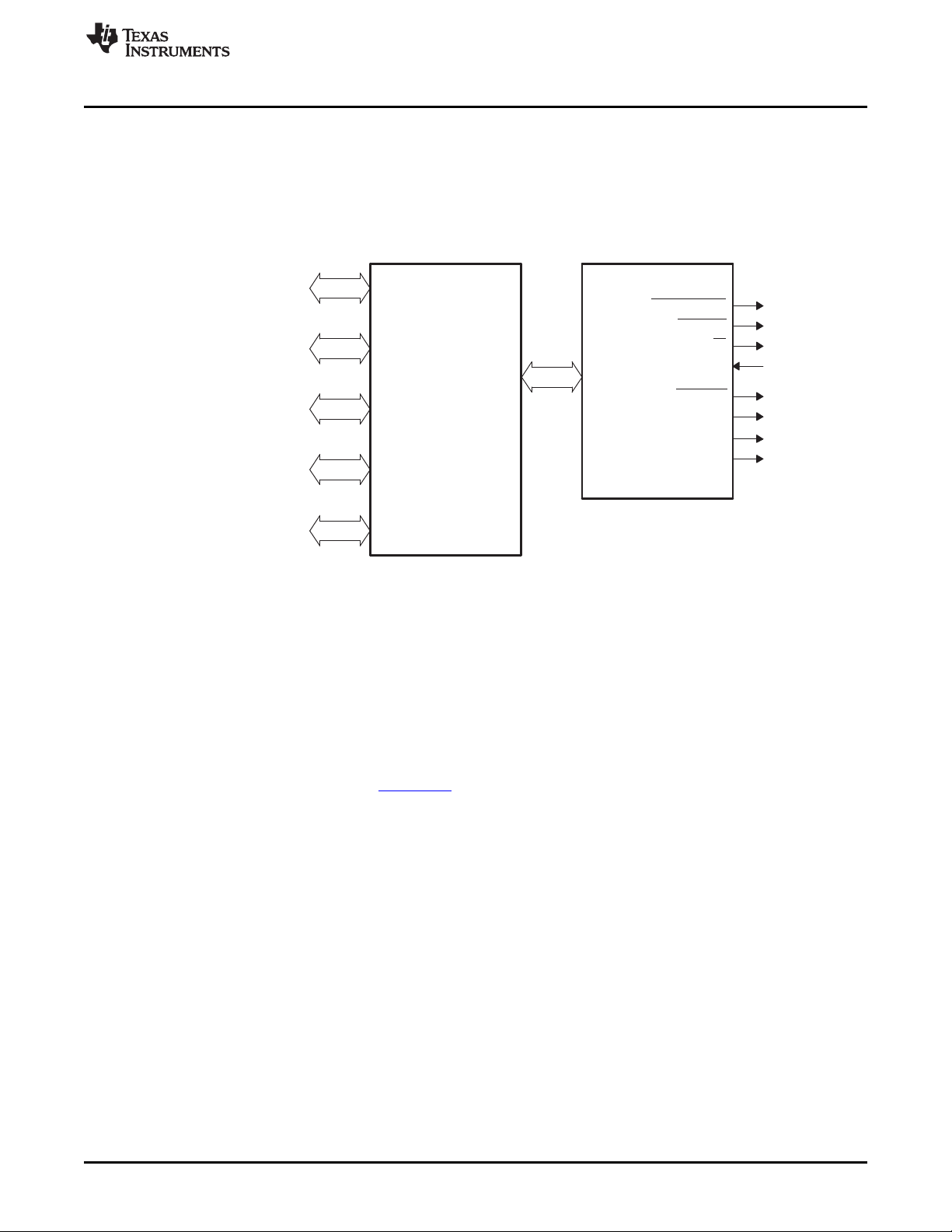
1.3 Functional Block Diagram
Figure 1 illustrates the connections between the EMIF and its internal requesters, along with the external
EMIF pins. Section 2.2 contains a description of the entities internal to the device that can send requests
to the EMIF, along with their prioritization. Section 2.3 describes the EMIF's external pins and summarizes
their purpose when interfacing with SDRAM and asynchronous devices.
Figure 1. EMIF Functional Block Diagram
Architecture
2 Architecture
This section provides details about the architecture and operation of the EMIF.
2.1 Clock Control
The EMIF's internal clock is sourced from the SYSCLK3 clock domain of PLL controller 0 and cannot be
sourced directly from an external input clock. The frequency of the SYSCLK3 clock domain is the PLL0
frequency divided by 4. Changes to the frequency of the input clock to PLL controller 0 and to the PLL
controller 0 multiplier values alters the operating frequency of the EMIF. See the TMS320DM646x DMSoC
ARM Subsystem Reference Guide (SPRUEP9) for more information on how to program the PLL
controller.
2.2 EMIF Requests
Four different sources within the device can make requests to the EMIF. These requests consist of
accesses to asynchronous memory and EMIF memory-mapped registers. Because the EMIF can process
only one request at a time, a high performance switched central resource (SCR) exists to provide
prioritized requests from the different sources to the EMIF. Each requester has a programmable priority
value that may be configured in the System Module MSTPRI0 register or in the EDMACC QUEPRI
register. See the device-specific data manual for more information.
If a request is submitted from two or more sources simultaneously, the SCR will forward the highest
priority request to the EMIF first. Upon completion of a request, the SCR again evaluates the pending
requests and forwards the highest priority pending request to the EMIF.
SPRUEQ7C–February 2010 Asynchronous External Memory Interface (EMIF)
Submit Documentation Feedback
9
Copyright © 2010, Texas Instruments Incorporated
Page 10

Architecture
2.3 Signal Descriptions
Table 1 describes the function of each of the EMIF pins.
Pins(s) I/O Description
EM_ A[22:0] O EMIF address bus. These pins are used in conjunction with the EM_BA pins to form the address that is
EM_BA[1:0] O EMIF bank address. These pins are used in conjunction with the EM_A pins to form the address that is
EM_CS[5:2] O Active-low chip enable pin for asynchronous devices. These pins are meant to be connected to the
EM_D[15:0] I/O EMIF data bus.
EM_RW O Read/Write select pin. This pin is high for the duration of an asynchronous read access cycle and low
EM_OE O Active-low pin enable for asynchronous devices. This pin provides a signal which is active-low during
EM_WE O Active-low write enable. This pin provides a signal which is active-low during the strobe period of an
EM_WAIT[5:2] I Wait input with programmable polarity. A connected asynchronous device can extend the strobe period
www.ti.com
Table 1. EMIF Pins
sent to the device.
sent to the device.
chip-select pin of the attached asynchronous device.
for the duration of an asynchronous write cycle.
the strobe period of an asynchronous read access cycle.
asynchronous write access cycle.
of an access cycle by asserting the WAIT input to the EMIF as described in Section 2.5.8. To enable
this functionality, the EW bit in the asynchronous configuration register (ACFGn) must be set to 1. In
addition, the WPn bit in the asynchronous wait cycle configuration register (AWCCR) must be
configured to define the polarity of the EM_WAITn pin.
2.4 Pin Multiplexing
The EMIF pins are multiplexed with other peripherals such as PCI, HPI, GPIO, and ATA. See the
device-specific data manual for instructions on how to select the EMIF pins for proper operation.
2.5 Asynchronous Controller and Interface
The EMIF easily interfaces to a variety of asynchronous devices including Flash and ASRAM. It can be
operated in three major modes:
• Normal mode
• Select Strobe (SS) mode
• NAND Flash mode
The behavior of the EM_CS signal is the single difference between Normal mode and Select Strobe mode
(see Table 2). In Normal mode, the EM_CS signal becomes active at the beginning of the setup period
and remains active for the duration of the transfer. In Select Strobe mode, the EM_CS signal functions as
a strobe signal, active only during the strobe period of an access.
In NAND Flash mode, the EMIF hardware is able to calculate the error correction code (ECC) for each
512 byte data transfer. In addition to the three modes of operation, the EMIF also provides configurable
cycle timing parameters and an Extended Wait mode that allows the connected device to extend the
strobe period of an access cycle. The following sections describe the features related to interfacing with
external asynchronous devices.
Table 2. Behavior of EM_CS Signal Between Normal Mode and
Select Strobe Mode
Mode Operation of EM_CS[5:2]
Normal Active during the entire asynchronous access cycle
Select Strobe Active only during the strobe period of an access cycle
10
Asynchronous External Memory Interface (EMIF) SPRUEQ7C–February 2010
Submit Documentation Feedback
Copyright © 2010, Texas Instruments Incorporated
Page 11
EM_CS[5:2]
EM_WE
EM_OE
EM_RW
EM_WAIT[5:2]
EM_BA[1:0]
EM_D[15:0]
EM_A[22:0]
EMIF
EM_D[7:0]
EM_A[21:0]
EM_BA[1:0]
DQ[7:0]
A[23:2]
A[1:0]
EMIF 8−bit
asynchronous
memory
a) EMIF to 8-bit memory interface
EM_D[15:0]
EM_A[21:0]
EM_BA[1]
DQ[15:0]
A[22:1]
A[0]
EMIF 16−bit
asynchronous
memory
b) EMIF to 16-bit memory interface
www.ti.com
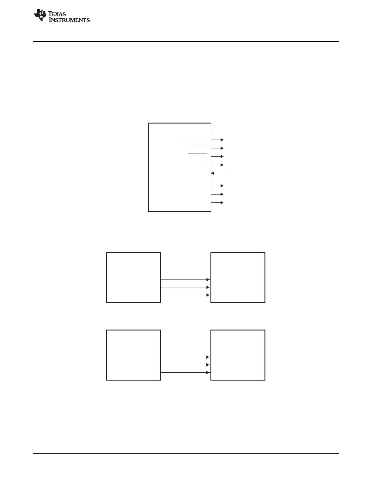
2.5.1 Interfacing to Asynchronous Memory
Figure 2 shows the EMIF's external pins used in interfacing with an asynchronous device. Of special note
is the connection between the EMIF and the external device's address bus. The EMIF address pin
EM_A[0] always provides the least significant bit of a 32-bit word address. Therefore, when interfacing to a
16-bit or 8-bit asynchronous device, the EM_BA[1] and EM_BA[0] pins provide the least-significant bits of
the halfword or byte address, respectively. Figure 2 and Figure 3 show the mapping between the EMIF
and the connected device's data and address pins for various programmed data bus widths. The data bus
width may be configured in the asynchronous configuration register (ACFGn).
Figure 2. EMIF Asynchronous Interface
Architecture
Figure 3. EMIF to 8-bit and 16-bit Memory Interfaces
SPRUEQ7C–February 2010 Asynchronous External Memory Interface (EMIF)
Submit Documentation Feedback
Copyright © 2010, Texas Instruments Incorporated
11
Page 12

Architecture
2.5.2 Programmable Asynchronous Parameters
The EMIF allows a high degree of programmability for shaping asynchronous accesses. The
programmable parameters are:
• Setup: The time between the beginning of a memory cycle (address valid) and the activation of the
output enable or write enable strobe
• Strobe: The time between the activation and deactivation of output enable or write enable strobe.
• Hold: The time between the deactivation of output enable or write enable strobe and the end of the
cycle, which may be indicated by an address change or the deactivation of the EM_CS signal.
Separate parameters are provided for read and write cycles. Each parameter is programmed in terms of
EMIF clock cycles.
2.5.3 Configuring the EMIF for Asynchronous Accesses
The operation of the EMIF's asynchronous interface can be configured by programming the appropriate
memory-mapped registers. The reset value and bit position for each register field can be found in
Section 4. The following tables list the programmable register fields and describe the purpose of each
field. These registers should not be programmed while an asynchronous access is in progress. The
transfer following a write to these registers will use the new configuration.
Table 3 describes the asynchronous configuration register (ACFGn). There are four ACFGns. Each chip
select space has a dedicated ACFGn. This allows each chip select space to be programmed
independently to interface to different asynchronous memory types.
www.ti.com
Table 3. Description of the Asynchronous Configuration Register (ACFGn)
Parameter Description
SS Select Strobe mode. This bit selects the EMIF's mode of operation in the following way:
• SS = 0 selects Normal mode. EM_CS is active for duration of access.
• SS = 1 selects Select Strobe mode. EM_CS acts as a strobe.
EW Extended Wait mode enable.
• EW = 0 disables Extended Wait mode
• EW = 1 enables Extended Wait mode
When set to 1, the EMIF enables its Extended Wait mode in which the strobe width of an access
cycle can be extended in response to the assertion of the EM_WAIT[5:2] pins. The WPn bit in the
asynchronous wait cycle configuration register (AWCCR) controls the polarity of the EM_WAITn pin.
See Section 2.5.8 for more details on this mode of operation.
W_SETUP/R_SETUP Read/Write setup widths.
W_STROBE/R_STROBE Read/Write strobe widths.
W_HOLD/R_HOLD Read/Write hold widths.
TA Minimum turnaround time.
These fields define the number of EMIF clock cycles of setup time for the address pins (EM_A and
EM_BA) and asynchronous chip enable (EM_CS) before the read strobe pin (READ_OE) or write
strobe pin (WRITE_WE) falls, minus 1 cycle. For writes, the W_SETUP field also defines the setup
time for the data pins (EM_D). Refer to the datasheet of the external asynchronous device to
determine the appropriate setting for this field.
These fields define the number of EMIF clock cycles between the falling and rising of the read strobe
pin (READ_OE) or write strobe pin (WRITE_WE), minus 1 cycle. If Extended Wait mode is enabled
by setting the EW bit in the asynchronous configuration register (ACFGn), these fields must be set to
a value greater than zero. Refer to the datasheet of the external asynchronous device to determine
the appropriate setting for this field.
These fields define the number of EMIF clock cycles of hold time for the address pins (EM_A and
EM_BA) and asynchronous chip enable (EM_CS) after the read strobe pin (READ_OE) or write
strobe pin (WRITE_WE) rises, minus 1 cycle. For writes, the W_HOLD field also defines the hold
time for the data pins (EM_D). Refer to the datasheet of the external asynchronous device to
determine the appropriate setting for this field.
This field defines the minimum number of EMIF clock cycles between the end of one asynchronous
access and the start of another, minus 1 cycle. This delay is not incurred when a read is followed by
a read, or a write is followed by a write to the same chip select space. The purpose of this feature is
to avoid contention on the bus. Refer to the datasheet of the external asynchronous device to
determine the appropriate setting for this field.
12
Asynchronous External Memory Interface (EMIF) SPRUEQ7C–February 2010
Copyright © 2010, Texas Instruments Incorporated
Submit Documentation Feedback
Page 13

www.ti.com
Architecture
Table 3. Description of the Asynchronous Configuration Register (ACFGn) (continued)
Parameter Description
ASIZE Asynchronous Device Bus Width.
This field determines the data bus width of the asynchronous interface in the following way:
• ASIZE = 0 selects an 8-bit bus
• ASIZE = 1 selects a 16-bit bus
The configuration of ASIZE determines the function of the EM_A and EM_BA pins as described in
Section 2.5.1. This field also determines the number of external accesses required to fulfill a request
generated by one of the sources mentioned in Section 2.2. For example, a request for a 32-bit word
would require four external access when ASIZE = 0h. Refer to the datasheet of the external
asynchronous device to determine the appropriate setting for this field.
Table 4. Description of the Asynchronous Wait Cycle Configuration Register (AWCCR)
Parameter Description
WPn WAIT Polarity.
• WPn = 0 selects active-low polarity
• WPn = 1 selects active-high polarity
When set to 1, the EMIF will wait if the EM_WAITn pin is high. When cleared to 0, the EMIF will wait if the
EM_WAITn pin is low. The EMIF must have the Extended Wait mode enabled (EW bit in the asynchronous
configuration register (ACFGn) is set to 1) for the EM_WAITn pin to affect the width of the strobe period.
MEWC Maximum Extended Wait Cycles.
This field configures the number of EMIF clock cycles the EMIF will wait for the EM_WAITn pin to be deactivated
during the strobe period of an access cycle. The maximum number of EMIF clock cycles the EMIF will wait is
determined by the following formula:
Maximum Extended Wait Cycles = (MEWC + 1) × 16
If the EM_WAITn pin is not deactivated within the time specified by this field, the EMIF resumes the access cycle,
registering whatever data is on the bus and preceding to the hold period of the access cycle. This situation is
referred to as an asynchronous timeout. An asynchronous timeout generates an interrupt if it has been enabled in
the EMIF interrupt mask set register (EIMSR). Refer to Section 2.5.11 for more information about the EMIF
interrupts.
Table 5. Description of the EMIF Interrupt Mask Set Register (EIMSR)
Parameter Description
WRMSETn Wait Rise Mask Set.
Writing a 1 enables an interrupt to be generated when a rising edge on EM_WAITn occurs.
ATMSET Asynchronous Timeout Mask Set.
Writing a 1 to this bit enables an interrupt to be generated when an asynchronous timeout occurs.
Table 6. Description of the EMIF Interrupt Mast Clear Register (EIMCR)
Parameter Description
WRMCLRn Wait Rise Mask Clear.
Writing a 1 to this bit disables the interrupt, clearing the WRMSETn bit in the EMIF interrupt mask set register
(EIMSR).
ATMCLR Asynchronous Timeout Mask Clear.
Writing a 1 to this bit disables the interrupt, clearing the ATMSET bit in the EMIF interrupt mask set register
(EIMSR).
SPRUEQ7C–February 2010 Asynchronous External Memory Interface (EMIF)
Submit Documentation Feedback
Copyright © 2010, Texas Instruments Incorporated
13
Page 14

Architecture
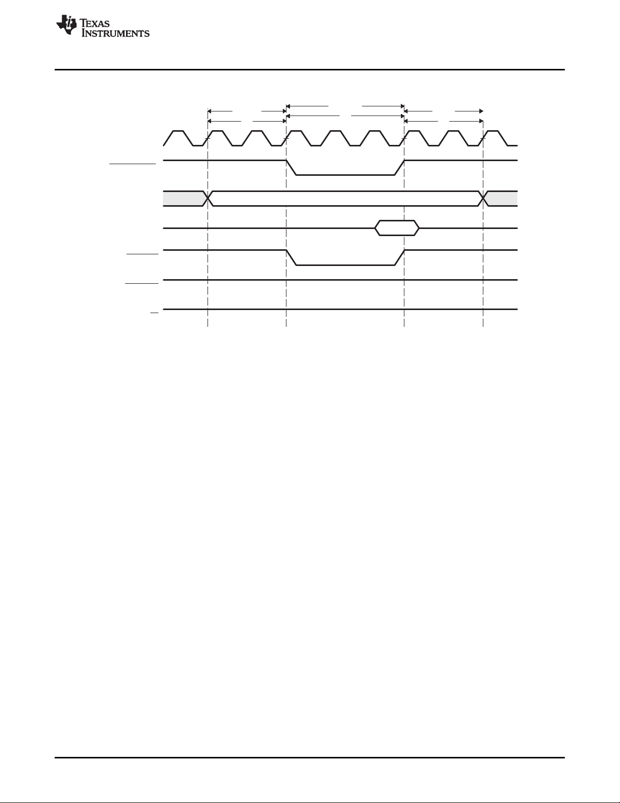
2.5.4 Read and Write Operations in Normal Mode
Normal mode is the asynchronous interface's default mode of operation. The Normal mode is selected
when the SS bit in the asynchronous configuration register (ACFGn) is cleared to 0. In this mode, the
EM_CS signal operates as a chip enable signal, active throughout the duration of the memory access.
2.5.4.1 Asynchronous Read Operations (Normal Mode)
An asynchronous read is performed when any of the requesters mentioned in Section 2.2 request a read
from the attached asynchronous memory. In the event that the read request cannot be serviced by a
single access cycle to the external device, multiple access cycles will be performed by the EMIF until the
entire request is fulfilled. The details of an asynchronous read operation in Normal mode are described in
Table 7 and an example timing diagram of a basic read operation is shown in Figure 4.
NOTE: During the entirety of an asynchronous read operation, the WRITE_WE and EM_RW pins
are driven high.
Table 7. Asynchronous Read Operation in Normal Mode
Time Interval Pin Activity in WE Strobe Mode
Turnaround Once the EMIF receives a read request, the EMIF waits for the programmed number of turn-around cycles
period before proceeding to the setup period of the operation. The number of wait cycles is taken directly from the TA
Start of setup At the beginning of the setup period:
period
Start of strobe At the beginning of the strobe period
period
Start of hold At the beginning of the hold period:
period
End of hold At the end of the hold period:
period
field of the asynchronous configuration register (ACFGn). There are two exceptions to this rule:
• If the current read operation was directly proceeded by another read operation to the same CS space, no
turnaround cycles are inserted.
• If the current read operation was not directly proceeded by a read operation to the same CS space and the
TA field has been cleared to 0, one turn-around cycle will be inserted.
After the EMIF has waited for the turnaround cycles to complete, it proceeds to the setup period of the operation.
• The setup, strobe, and hold values are set according to the R_SETUP, R_STROBE, and R_HOLD values
in ACFGn.
• The address pins EM_A and EM_BA become valid
• EM_CS falls to enable the external device (if not already low from a previous operation)
• READ_OE falls
• READ_OE rises
• The EMIF samples the data on the EM_D bus.
• The address pins EM_A and EM_BA become invalid
• EM_CS rises (if no more operations are required to complete the current request)
The EMIF will be required to issue additional read operations to a device with a small data bus width in order to
complete an entire word access. In this case, the EMIF immediately re-enters the setup period to begin another
operation without incurring the turn-round cycle delay. The setup, strobe, and hold values are not updated in this
case. If the entire word access has been completed, the EMIF returns to its previous state unless another
asynchronous request has been submitted and is currently the highest priority task. If this is the case, the EMIF
instead enters directly into the turnaround period for the pending read or write operation.
www.ti.com
14
Asynchronous External Memory Interface (EMIF) SPRUEQ7C–February 2010
Copyright © 2010, Texas Instruments Incorporated
Submit Documentation Feedback
Page 15
Internal clock
EM_CS[5:2]
EM_A/EM_BA
EM_D
EM_OE
EM_WE
EM_RW
Setup
Strobe
Hold
2
3
2
Address
Data
www.ti.com
Architecture
Figure 4. Timing Waveform of an Asynchronous Read Cycle in Normal Mode
SPRUEQ7C–February 2010 Asynchronous External Memory Interface (EMIF)
Submit Documentation Feedback
Copyright © 2010, Texas Instruments Incorporated
15
Page 16

Architecture
2.5.4.2 Asynchronous Write Operations (Normal Mode)
An asynchronous write is performed when any of the requesters mentioned in Section 2.2 request a write
to asynchronous memory. In the event that the write request cannot be serviced by a single access cycle
to the external device, multiple access cycles will be performed by the EMIF until the entire request is
fulfilled. The details of an asynchronous write operation in Normal mode are described in Table 8 and an
example timing diagram of a basic write operation is shown in Figure 5.
NOTE: During the entirety of an asynchronous write operation, the EM_OE pin is driven high.
Table 8. Asynchronous Write Operation in Normal Mode
Time Interval Pin Activity in WE Strobe Mode
Turnaround Once the EMIF receives a write request, the EMIF waits for the programmed number of turn-around cycles
period before proceeding to the setup period of the operation. The number of wait cycles is taken directly from the TA
Start of setup At the beginning of the setup period:
period
Start of strobe At the beginning of the strobe period of a write operation:
period
Start of hold At the beginning of the hold period
period
End of hold At the end of the hold period:
period
field of the asynchronous configuration register (ACFGn). There are two exceptions to this rule:
• If the current write operation was directly proceeded by another write operation to the same CS space, no
turnaround cycles are inserted.
• If the current write operation was not directly proceeded by a write operation to the same CS space and the
TA field has been cleared to 0, one turnaround cycle will be inserted.
After the EMIF has waited for the turnaround cycles to complete, it proceeds to the setup period of the operation.
• The setup, strobe, and hold values are set according to the W_SETUP, W_STROBE, and W_HOLD values
in ACFGn.
• The address pins EM_A and EM_BA and the data pins EM_D become valid.
• The EM_RW pin falls to indicate a write (if not already low from a previous operation).
• EM_CS falls to enable the external device (if not already low from a previous operation).
• EM_WE falls
• EM_WE rises
• The address pins EM_A and EM_BA become invalid
• The data pins become invalid
• The EM_RW pin rises (if no more operations are required to complete the current request)
• EM_CS rises (if no more operations are required to complete the current request)
The EMIF may be required to issue additional write operations to a device with a small data bus width in order to
complete an entire word access. In this case, the EMIF immediately re-enters the setup period to begin another
operation without incurring the turnaround cycle delay. The setup, strobe, and hold values are not updated in this
case. If the entire word access has been completed, the EMIF returns to its previous state unless another
asynchronous request has been submitted. If this is the case, the EMIF instead enters directly into the
turnaround period for the pending read or write operation.
www.ti.com
16
Asynchronous External Memory Interface (EMIF) SPRUEQ7C–February 2010
Copyright © 2010, Texas Instruments Incorporated
Submit Documentation Feedback
Page 17
Internal clock
EM_CS[5:2]
EM_A/EM_BA
EM_D
EM_OE
EM_WE
EM_RW
Setup
Strobe
Hold
2
3
2
Address
Data
www.ti.com
Architecture
Figure 5. Timing Waveform of an Asynchronous Write Cycle in Normal Mode
SPRUEQ7C–February 2010 Asynchronous External Memory Interface (EMIF)
Submit Documentation Feedback
Copyright © 2010, Texas Instruments Incorporated
17
Page 18

Architecture
2.5.5 Read and Write Operations in Select Strobe Mode
Select Strobe mode is the EMIF's second mode of operation. The SS mode is selected when the SS bit in
the asynchronous configuration register (ACFGn) is set to 1. In this mode, the EM_CS pin functions as a
strobe signal and is therefore only active during the strobe period of an access cycle.
2.5.5.1 Asynchronous Read Operations (Select Strobe Mode)
An asynchronous read is performed when any of the requesters mentioned in Section 2.2 request a read
from the attached asynchronous memory. In the event that the read request cannot be serviced by a
single access cycle to the external device, multiple access cycles will be performed by the EMIF until the
entire request is fulfilled. The details of an asynchronous read operation in Select Strobe mode are
described in Table 9 and an example timing diagram of a basic read operation is shown in Figure 6.
NOTE: During the entirety of an asynchronous read operation, the EM_WE and EM_RW pins are
driven high.
Table 9. Asynchronous Read Operation in Select Strobe Mode
Time Interval Pin Activity in Select Strobe Mode
Turnaround Once the EMIF receives a read request, the EMIF waits for the programmed number of turnaround cycles before
period proceeding to the setup period of the operation. The number of wait cycles is taken directly from the TA field of
Start of setup At the beginning of the setup period:
period
Start of strobe At the beginning of the strobe period:
period
Start of hold At the beginning of the hold period:
period
End of hold At the end of the hold period:
period
the asynchronous configuration register (ACFGn). There are two exceptions to this rule:
• If the current read operation was directly proceeded by another read operation to the same CS space, no
turnaround cycles are inserted.
• If the current read operation was not directly proceeded by a read operation to the same CS space and the
TA field has been cleared to 0, one turnaround cycle will be inserted.
After the EMIF has waited for the turnaround cycles to complete, it proceeds to the setup period of the operation.
• The setup, strobe, and hold values are set according to the R_SETUP, R_STROBE, and R_HOLD values
in ACFGn.
• The address pins EM_A and EM_BA become valid.
• EM_CS and EM_OE fall at the start of the strobe period
• EM_CS and EM_OE rise
• The EMIF samples the data on the EM_D bus
• The address pins EM_A and EM_BA become invalid
The EMIF may be required to issue additional read operations to a device with a small data bus width in order to
complete an entire word access. In this case, the EMIF immediately re-enters the setup period to begin another
operation without incurring the turnaround cycle delay. The setup, strobe, and hold values are not updated in this
case. If the entire word access has been completed, the EMIF returns to its previous state unless another
asynchronous request has been submitted. If this is the case, the EMIF instead enters directly into the
turnaround period for the pending read or write operation.
www.ti.com
18
Asynchronous External Memory Interface (EMIF) SPRUEQ7C–February 2010
Copyright © 2010, Texas Instruments Incorporated
Submit Documentation Feedback
Page 19
Internal clock
EM_CS[5:2
]
EM_A/EM_BA
EM_D
EM_OE
EM_WE
EM_RW
Setup
Strobe
Hold
2
3
2
Address
Data
www.ti.com
Architecture
Figure 6. Timing Waveform of an Asynchronous Read Cycle in Select Strobe Mode
SPRUEQ7C–February 2010 Asynchronous External Memory Interface (EMIF)
Submit Documentation Feedback
Copyright © 2010, Texas Instruments Incorporated
19
Page 20

Architecture
2.5.5.2 Asynchronous Write Operations (Select Strobe Mode)
An asynchronous write is performed when any of the requesters mentioned in Section 2.2 request a write
to memory in the asynchronous bank of the EMIF. In the event that the write request cannot be serviced
by a single access cycle to the external device, multiple access cycles will be performed by the EMIF until
the entire request is fulfilled. The details of an asynchronous write operation in Select Strobe mode are
described in Table 10 and an example timing diagram of a basic write operation is shown in Figure 7.
NOTE: During the entirety of an asynchronous write operation, the EM_OE pin is driven high.
Table 10. Asynchronous Write Operation in Select Strobe Mode
Time Interval Pin Activity in Select Strobe Mode
Turnaround Once the EMIF receives a write request, the EMIF waits for the programmed number of turnaround cycles
period before proceeding to the setup period of the operation. The number of wait cycles is taken directly from the TA
Start of setup At the beginning of the setup period:
period
Start of strobe At the beginning of the strobe period:
period
Start of hold At the beginning of the hold period:
period
End of hold At the end of the hold period:
period
field of the asynchronous configuration register (ACFGn). There are two exceptions to this rule:
• If the current write operation was directly proceeded by another write operation to the same CS space, no
turnaround cycles are inserted.
• If the current write operation was directly proceeded by a write operation to the same CS space and the TA
field has been cleared to 0, one turnaround cycle will be inserted.
After the EMIF has waited for the turnaround cycles to complete, it proceeds to the setup period of the operation.
• The setup, strobe, and hold values are set according to the W_SETUP, W_STROBE, and W_HOLD values
in ACFGn.
• The address pins EM_A and EM_BA and the data pins EM_D become valid.
• The EM_RW pin falls to indicate a write (if not already low from a previous operation).
• EM_CS and EM_WE fall
• EM_CS and EM_WE rise
• The address pins EM_A and EM_BA become invalid
• The data pins become invalid
• The EM_RW pin rises (if no more operations are required to complete the current request)
The EMIF may be required to issue additional write operations to a device with a small data bus width in order to
complete an entire word access. In this case, the EMIF immediately re-enters the setup period to begin another
operation without incurring the turnaround cycle delay. The setup, strobe, and hold values are not updated in this
case. If the entire word access has been completed, the EMIF returns to its previous state unless another
asynchronous request has been submitted. If this is the case, the EMIF instead enters directly into the
turn-around period for the pending read or write operation.
www.ti.com
20
Asynchronous External Memory Interface (EMIF) SPRUEQ7C–February 2010
Copyright © 2010, Texas Instruments Incorporated
Submit Documentation Feedback
Page 21

Internal clock
EM_CS[5:2
]
EM_A/EM_BA
EM_D
EM_OE
EM_WE
EM_RW
Setup
Strobe
Hold
2
3
2
Address
Data
www.ti.com
Architecture
Figure 7. Timing Waveform of an Asynchronous Write Cycle in Select Strobe Mode
SPRUEQ7C–February 2010 Asynchronous External Memory Interface (EMIF)
Submit Documentation Feedback
Copyright © 2010, Texas Instruments Incorporated
21
Page 22

Architecture
2.5.6 NAND Flash Mode
NAND Flash mode is the EMIF's third mode of operation. Each chip select space may be placed in NAND
Flash mode individually by setting the appropriate CSnNAND bit in the NAND Flash control register
(NANDFCR). Table 11 displays the bit fields present in NANDFCR and briefly describes their use.
When a chip select space is configured to operate in NAND Flash mode, the EMIF hardware can calculate
the error correction code (ECC) for each 512 byte data transfer to that chip select space. The EMIF
hardware will not generate the NAND access cycle, which includes the command, address, and data
phases, necessary to complete a transfer to NAND Flash. All NAND Flash operations can be divided into
single asynchronous cycles and with the help of software, the EMIF can execute a complete NAND
access cycle.
Table 11. Description of the NAND Flash Control Register (NANDFCR)
Parameter Description
CS5ECC NAND Flash ECC state for chip select 5.
• Set to 1 to start an ECC calculation.
• Cleared to 0 when NAND Flash 4 ECC register (NANDF4ECC) is read.
CS4ECC NAND Flash ECC state for chip select 4.
• Set to 1 to start an ECC calculation.
• Cleared to 0 when NAND Flash 3 ECC register (NANDF3ECC) is read.
CS3ECC NAND Flash ECC state for chip select 3.
• Set to 1 to start an ECC calculation.
• Cleared to 0 when NAND Flash 2 ECC register (NANDF2ECC) is read.
CS2ECC NAND Flash ECC state for chip select 2.
• Set to 1 to start an ECC calculation.
• Cleared to 0 when NAND Flash 1 ECC register (NANDF1ECC) is read.
CS5NAND NAND Flash mode for chip select 5.
• Set to 1 to enable NAND Flash mode.
CS4NAND NAND Flash mode for chip select 4.
• Set to 1 to enable NAND Flash mode.
CS3NAND NAND Flash mode for chip select 3.
• Set to 1 to enable NAND Flash mode.
CS2NAND NAND Flash mode for chip select 2.
• Set to 1 to enable NAND Flash mode.
www.ti.com
2.5.6.1 Configuring for NAND Flash Mode
Similar to the asynchronous accesses previously described, the EMIF's memory-mapped registers must
be programmed appropriately to interface to a NAND Flash device. Table 12 lists the bit fields that must
be programmed when operating in NAND Flash mode and the values to set each bit. NAND Flash mode
cannot be used with Extended Wait mode.
Table 12. Configuration For NAND Flash
Register Bit Field Configuration Value
Asynchronous configuration SS 0
register (ACFGn)
NAND Flash control register CS2NAND 1
(NANDFCR)
22
Asynchronous External Memory Interface (EMIF) SPRUEQ7C–February 2010
EW 0
W_SETUP/R_SETUP See Section 3.2 for information on how to program.
W_STROBE/R_STROBE See Section 3.2 for information on how to program.
W_HOLD/R_HOLD See Section 3.2 for information on how to program.
ASIZE Programmed to equal the width of the NAND Flash device
Submit Documentation Feedback
Copyright © 2010, Texas Instruments Incorporated
Page 23

CLE_EM_A[16]
ALE_EM_A[17]
EM_CS[n]
EM_WE
EM_OE
EM_D[7:0]
EM_WAIT[n]
EMIF
CLE
ALE
CE
WE
OE
IO[7:0]
R/B
NAND flash
a) Connection to 8-bit NAND device
b) Connection to 16-bit NAND device
EM_WAIT[n]
EM_D[15:0]
EM_OE
EM_WE
EM_CS[n]
ALE_EM_A[17]
CLE_EM_A[16]
EMIF
CE
IO[15:0]
R/B
OE
WE
NAND flash
CLE
ALE
www.ti.com
2.5.6.2 Connecting to NAND Flash
Figure 8 shows the EMIF external pins used to interface with a NAND Flash device. EMIF address lines
are used to drive the NAND Flash device's command latch enable (CLE) and address latch enable (ALE)
signals.
NOTE: The EMIF will not control the NAND Flash device's write protect pin. The write protect pin
must be controlled outside of the EMIF.
Figure 8. EMIF to NAND Flash Interface
Architecture
2.5.6.3 Driving CLE and ALE
As stated in Section 2.5.1, the EMIF always drives the least significant bit of a 32-bit word address on
EM_A[0]. This functionality must be considered when attempting to drive the address lines connected to
CLE and ALE to the appropriate state.
For example, if using EM_A[2] and EM_A[1] to connect to CLE and ALE, respectively, the following offsets
should be chosen:
• 00h to drive CLE and ALE low
• 10h to drive CLE high and ALE low
• 0Bh to drive CLE low and ALE high
These offsets should be added to the base address for the chip select space the NAND Flash device is
connected to. For example, if the base address of the CS space the NAND Flash device is connected to is
4200 0000h, then the above list translates to the following memory-mapped addresses: 4200 0000h, 4200
0010h, and 4200 000Bh, respectively. Therefore, when attempting to drive CLE high and ALE low, the
memory-mapped address of 4200 0010h would be written to.
SPRUEQ7C–February 2010 Asynchronous External Memory Interface (EMIF)
Submit Documentation Feedback
23
Copyright © 2010, Texas Instruments Incorporated
Page 24

Architecture
2.5.6.4 NAND Read and Program Operations
A NAND Flash access cycle is composed of a command, address, and data phase. The EMIF will not
automatically generate these three phases to complete a NAND access with one transfer request. To
complete a NAND access cycle, multiple single asynchronous access cycles (as described above) must
be completed by the EMIF. Software must be used to request the appropriate asynchronous accesses to
complete a NAND Flash access cycle. This software must be developed to the specification of the chosen
NAND Flash device.
Since NAND operations are divided into single asynchronous access cycles, the chip select signal will not
remain activated for the duration of the NAND operation. Instead, the chip select signal will deactivate
between each asynchronous access cycle. For this reason, the EMIF does not support NAND Flash
devices that require the chip select signal to remain low during the tRtime for a read. See Section 2.5.6.8
for workaround.
Care must be taken when performing a NAND read or write operation via the EDMA. See Section 2.5.6.5
for more details.
NOTE: The EMIF does not support NAND Flash devices that require the chip select signal to
remain low during the tRtime for a read. See Section 2.5.6.8 for workaround.
2.5.6.5 NAND Data Read and Write via DMA
When performing NAND accesses, the EDMA is most efficiently used for the data phase of the access.
The command and address phases of the NAND access require only a few words of data to be
transferred and therefore do not take advantage of the EDMA's ability to transfer larger quantities of data
with a single request. In this section we will focus on using the EDMA for the data phase of a NAND
access.
There are two conditions that require care to be taken when performing NAND reads and writes via the
EDMA. These are:
• CLE_EM_A[2] and ALE_EM_A[1] are lower address lines and must be driven low
• The EMIF does not support a constant address mode, but only supports linear incrementing address
modes.
Since the EMIF does not support a constant addressing mode, when programming the EDMA, a linear
incrementing address mode must be used. When using a linear incrementing address mode, since the
CLE and ALE are driven by lower address lines, care must be taken not to increase the address into a
range the drives CLE and/or ALE high. To prevent the address from incrementing into a range that drives
CLE and/or ALE high, the EDMA ACNT, BCNT, SIDX, DIDX, and synchronization type must be
programmed appropriately. The proper EDMA configurations are described below.
EDMA setup for a NAND Flash data read:
• ACNT ≤ 8 bytes (this can also be set to less than or equal to the external data bus width)
• BCNT = transfer size in bytes/ACNT
• SIDX (source index) = 0
• DIDX (destination index) = ACNT
• AB synchronized
EDMA setup for a NAND Flash data write:
• ACNT ≤ 8 bytes (this can also be set to less than or equal to the external data bus width)
• BCNT = transfer size in bytes/ACNT
• SIDX (source index) = ACNT
• DIDX (destination index) = 0
• AB synchronized
www.ti.com
24
Asynchronous External Memory Interface (EMIF) SPRUEQ7C–February 2010
Submit Documentation Feedback
Copyright © 2010, Texas Instruments Incorporated
Page 25

Bit 7
Bit 7
Bit 7
Bit 7
Bit 6 Bit 5 Bit 4 Bit 3 Bit 2 Bit 1 Bit 0
Bit 6
Bit 5 Bit 4 Bit 2Bit 3 Bit 1 Bit 0
Bit 6
Bit 6
Bit 1Bit 3 Bit 2Bit 4Bit 5
Bit 5 Bit 4 Bit 2Bit 3 Bit 1
Bit 0
Bit 0
p8o
p8o
p8e
p8e
p16e
p16o
p32e
Byte 1
Byte 2
Byte 3
Byte 4
Bit 6
Bit 6
Bit 6
Bit 6
Byte 2 Bit 7
Byte 4
Byte 3
Bit 7
Bit 7
Byte 1 Bit 7
Bit 1Bit 3 Bit 2Bit 4Bit 5
Bit 5
Bit 5 Bit 4
Bit 4 Bit 2
Bit 2Bit 3
Bit 3
Bit 1
Bit 1
Bit 5 Bit 4 Bit 2Bit 3 Bit 1
p16e
p8o
Bit 0
p16o
Bit 0
Bit 0
p8o
p8e
p32o
Bit 0
p8e
p2048e
p2048o
p1o p1e p1ep1o p1ep1o p1o p1e
p2o p2e p2o p2e
p4o p4e
www.ti.com
2.5.6.6 ECC Generation
If the CSnNAND bit in the NAND Flash control register (NANDFCR) is set to 1, the EMIF supports ECC
calculation for up to 512 bytes for the corresponding chip select care. To perform the ECC calculation, the
CS2ECC bit in NANDFCR must be set to 1. The ECC calculation for each chip select space is
independent of each other. It is the responsibility of the software to start the ECC calculation by writing to
the CS2ECC bit prior to issuing a write or read to NAND Flash. It is also the responsibility of the software
to read the calculated ECC from the NAND Flash 1 ECC register (NANDF1ECC) once the transfer to
NAND Flash has completed. If the software writes or reads more than 512 bytes, the ECC will be
incorrect. There is a NANDECCn for each chip select space and when read, the corresponding CSnECC
bit in NANDFCR is cleared. The NANDF1ECC is cleared upon writing a 1 to the CS2ECC bit. Figure 9
shows the algorithm used to calculate the ECC value for an 8-bit NAND Flash.
For an 8-bit NAND Flash p1e through p4e are column parities and p8e through p2048 are row parities.
Similarly, the algorithm can be extended to a 16-bit NAND Flash. For a 16-bit NAND Flash p1e through
p8e are column parities and p16e through p2048 are row parities. The software must ignore the unwanted
parity bits if ECC is desired for less than 512 bytes of data. For example. p2048e and p2048o are not
required for ECC on 256 bytes of data. Similarly, p1024e, p1024o, p2048e, and p2048o are not required
for ECC on 128 bytes of data.
Architecture
Figure 9. ECC Value for 8-Bit NAND Flash
SPRUEQ7C–February 2010 Asynchronous External Memory Interface (EMIF)
Submit Documentation Feedback
Copyright © 2010, Texas Instruments Incorporated
25
Page 26

EM_D[15:0]
EM_RW
EM_A[1:0]
EM_WAIT
EM_OE
EM_WE
EM_CS
EM_BA1
GPIOx
AEMIF
HD[15:0]
HR/W
HCNTL[1:0]
HRDY
HDS1
HCS
HHWIL
HINT
HDS2
HAS
HPIENA
HBED
A
HBE1
A
HPI16
VCC
VCC
VSS
VSS
Architecture
2.5.6.7 NAND Flash Status Register (NANDFSR)
The NAND Flash status register (NANDFSR) indicates the raw status of the EM_WAITn pin. The
EM_WAITn pin should be connected to the NAND Flash device's R/B signal, so that it indicates whether
or not the NAND Flash device is busy. During a read, the R/B signal will transition and remain low while
the NAND Flash retrieves the data requested. Once the R/B signal transitions high, the requested data is
ready and should be read by the EMIF. During a write/program operation, the R/B signal transitions and
remains low while the NAND Flash is programming the Flash with the data it has received from the EMIF.
Once the R/B signal transitions high, the data has been written to the Flash and the next phase of the
transaction may be performed. From this explanation, you can see that the NAND Flash status register is
useful to the software for indicating the status of the NAND Flash device and determining when to proceed
to the next phase of a NAND Flash operation.
When a rising edge occurs on the EM_WAITn pin, the EMIF sets the WR (wait rise) bit in the EMIF
interrupt raw register (EIRR). Therefore, the EMIF wait rise interrupt may be used to indicate the status of
the NAND Flash device. The WPn bit in the asynchronous wait cycle configuration register (AWCCR)
does not affect the NAND Flash status register (NANDFSR) or the WRn bit in EIRR. See Section 2.5.11.1
for more a detailed description of the wait rise interrupt.
2.5.6.8 Interfacing to a Non-CE Don't Care NAND Flash
As explained in Section 2.5.6.4, the EMIF does not support NAND Flash devices that require the chip
select signal to remain low during the tRtime for a read. One way to work around this limitation is to use a
GPIO pin to drive the CE signal of the NAND Flash device. If this work around is implemented, software
will configure the selected GPIO to be low, then begin the NAND Flash operation, starting with the
command phase. Once the NAND Flash operation has completed the software will configure the selected
GPIO to be high. See Section 3 for more details on the GPIO workaround.
www.ti.com
2.5.7 Interfacing to a TI DSP HPI
The EMIF supports connecting as a host to a TI DSP HPI interface. When connecting to a TI DSP HPI
interface, the EMIF must be configured for normal mode operation. Figure 10 shows the connection
diagram.
Figure 10. EMIF to 16-Bit Multiplexed HPI16 Interface
A HBE signals may not be present on all HPI interfaces.
26
Asynchronous External Memory Interface (EMIF) SPRUEQ7C–February 2010
Copyright © 2010, Texas Instruments Incorporated
Submit Documentation Feedback
Page 27

www.ti.com
2.5.8 Extended Wait Mode and the EM_WAIT Pin
The Extended Wait mode is a mode in which the external asynchronous device may assert control over
the length of the strobe period. The Extended Wait mode can be entered by setting the EW bit in the
asynchronous configuration register (ACFGn). When the EW bit is set, the EMIF monitors the
EM_WAIT[5:2] pins to determine if the attached device wishes to extend the strobe period of the current
access cycle beyond the programmed number of clock cycles.
When the EMIF detects that the EM_WAIT pin has been asserted, it will begin inserting extra strobe
cycles into the operation until the EM_WAIT pin is deactivated by the external device. The EMIF will then
return to the last cycle of the programmed strobe period and the operation will proceed as usual from this
point. Refer to the device-specific data manual for details on the timing requirements of the EM_WAIT
signal.
The EM_WAIT pin cannot be used to extend the strobe period indefinitely. The programmable MEWC bit
in the asynchronous wait cycle configuration register (AWCCR) determines the maximum number of EMIF
clock cycles the strobe period may be extended beyond the programmed length. When the number of
cycles programmed in the MEWC bit expires, the EMIF proceeds to the hold period of the operation
regardless of the state of the EM_WAIT pin. The EMIF can also generate an interrupt upon expiration of
this counter. See Section 2.5.11.1 for details on enabling this interrupt.
For the EMIF to function properly in the Extended Wait mode, the WPn bit in AWCCR must be
programmed to match the polarity of the attached device. When the WPn bit is in its reset state of 1, the
EMIF will insert wait cycles when the EM_WAITn pin is sampled high; when the WPn bit is cleared to 0,
the EMIF will insert wait cycles only when the EM_WAITn pin is sampled low. This programmability allows
for a glueless connection to larger variety of asynchronous devices.
Finally, a restriction is placed on the setup and strobe period timing parameters when operating in
Extended Wait mode. Specifically, the sum of the W_SETUP and W_STROBE fields must be greater than
4, and the sum of the R_SETUP and R_STROBE fields must be greater than 4 for the EMIF to recognize
the EM_WAIT pin has been asserted. The W_SETUP, W_STROBE, R_SETUP, and R_STROBE fields
are in ACFGn.
Architecture
2.5.9 Data Bus Parking
The EMIF always drives the data bus to the previous write data value when it is idle. This feature is called
data bus parking. Only when the EMIF issues a read command to the external memory does it stop
driving the data bus. After the EMIF latches the last read data, it immediately parks the data bus again.
2.5.10 Reset and Initialization Considerations
The EMIF and its registers will be reset when any of the following events occur:
1. The RESET pin on the device is asserted
2. The EMIF is placed in reset by the Power and Sleep Controller.
When a reset occurs, the EMIF will immediately abandon any access request that is in progress and reset
all registers and internal logic to their default state.
Following device power up and deassertion of the RESET pin, the internal clock to the EMIF is turned on
and the EMIF memory-mapped registers are programmed to their default values.
SPRUEQ7C–February 2010 Asynchronous External Memory Interface (EMIF)
Submit Documentation Feedback
Copyright © 2010, Texas Instruments Incorporated
27
Page 28

Architecture
2.5.11 Interrupt Support
The EMIF has a single interrupt source (Table 13) mapped to the ARM interrupt controller. For more
information on the ARM interrupt controller (AINTC), see the TMS320DM646x DMSoC ARM Subsystem
Reference Guide (SPRUEP9).
The EMIF supports a single interrupt to the CPU. Section 2.5.11.1 details the generation and internal
masking of EMIF interrupts and Section 2.5.11.2 describes how the EMIF interrupts are sent to the CPU.
2.5.11.1 Interrupt Events
There are two conditions that may cause the EMIF to generate an interrupt to the CPU. These two
conditions are:
• A rising edge on the EM_WAIT signal (wait rise interrupt)
• An asynchronous time out
The wait rise interrupt is not affected by the WPn bit in the asynchronous wait cycle configuration register
(AWCCR). The asynchronous time out interrupt condition occurs when the attached asynchronous device
fails to deassert the EM_WAIT pin within the number of cycles defined by the MEWC bit in AWCCR.
Only when the interrupt is enabled by setting the appropriate bit (WRMSETn or ATMSET) in the EMIF
interrupt mask set register (EIMSR) to 1, will the interrupt be sent to the CPU. Once enabled, the interrupt
may be disabled by writing a 1 to the corresponding bit in the EMIF interrupt mask clear register (EIMCR).
The bit fields in both the EIMSR and EIMCR may be used to indicate whether the interrupt is enabled.
When the interrupt is enabled, the corresponding bit field in both the EIMSR and EIMCR will have a value
of 1; when the interrupt is disabled, the corresponding bit field will have a value of 0.
The EMIF interrupt raw register (EIRR) and the EMIF interrupt mask register (EIMR) indicate the status of
each interrupt. The appropriate bit (WRn or AT) in EIRR is set when the interrupt condition occurs,
whether or not the interrupt has been enabled. Whereas, the appropriate bit (WRMn or ATM) in EIMR is
set only when the interrupt condition occurs and the interrupt is enabled. Writing a 1 to the bit in EIRR
clears the EIRR bit as well as the corresponding bit in EIMR.
Table 14 contains a brief summary of the interrupt status and control bit fields. See Section 4 for complete
details on the register fields.
www.ti.com
Table 13. EMIF Interrupt
ARM Event Acronym Source
60 EMIFAINT EMIF
Table 14. Interrupt Monitor and Control Bit Fields
Register Name Bit Name Description
EMIF interrupt raw register WRn This bit is always set when an rising edge on the EM_WAIT signal occurs.
(EIRR) Writing a 1 clears the WRn bit as well as the WRMn bit in EIMR.
AT This bit is always set when an asynchronous timeout occurs. Writing a 1
EMIF interrupt mask register WRMn This bit is only set when a rising edge on the EM_WAIT signal occurs and
(EIMR) the interrupt has been enabled by writing a 1 to the WRMSETn bit in
ATM This bit is only set when an asynchronous timeout occurs and the interrupt
EMIF interrupt mask set register WRMSETn Writing a 1 to this bit enables the wait rise interrupt.
(EIMSR)
EMIF interrupt mask clear register WRMCLRn Writing a 1 to this bit disables the wait rise interrupt.
(EIMCR)
28
Asynchronous External Memory Interface (EMIF) SPRUEQ7C–February 2010
ATMSET Writing a 1 to this bit enables the asynchronous timeout interrupt.
ATMCLR Writing a 1 to this bit disables the asynchronous timeout interrupt.
Copyright © 2010, Texas Instruments Incorporated
clears the AT bit as well as the ATM bit in EIMR.
EIMSR.
has been enabled by writing a 1 to the ATMSET bit in EIMSR.
Submit Documentation Feedback
Page 29

www.ti.com
2.5.11.2 Interrupt Multiplexing
The EMIF interrupt is supported by both the ARM and DSP. The interrupt is not multiplexed with another
interrupt and is therefore always available.
2.5.12 Program Execution
Since the EMIF does not have byte enable or data mask pins, byte accesses to memory are not
supported when the data bus width is equal to 16 bits. When performing data accesses on a 16-bit bus,
this may be worked around by performing a write modify read back operation. When executing code from
the EMIF, the bus width must be configured to be an 8-bit data bus.
2.5.13 Power Management
Power dissipation to the EMIF may be managed by gating the input clock to the EMIF off. The input clock
is turned off outside of the EMIF through the use of the Power and Sleep Controller (PSC). When the PSC
sends a clock stop request to the EMIF, the EMIF will complete pending transfers before issuing a clock
stop acknowledge, allowing the PSC to stop the clock. See the TMS320DM646x DMSoC ARM Subsystem
Reference Guide (SPRUEP9) for more information.
2.5.14 Emulation Considerations
The operation of the EMIF is not affected when a breakpoint is reached or an emulation halt occurs.
Architecture
SPRUEQ7C–February 2010 Asynchronous External Memory Interface (EMIF)
Submit Documentation Feedback
Copyright © 2010, Texas Instruments Incorporated
29
Page 30

EM_CS
EM_WE
EM_OE
A[18:0]
EM_BA[1]
EM_D[15:0]
CE
WE
OE
LB
UB
A[19:1]
A[0]
DQ[15:0]
V
S S
V
SS
EMIF TC5516100FT−12
Use Cases
3 Use Cases
The EMIF allows a high degree of programmability for shaping asynchronous accesses. As previously
stated, the shape and duration of the asynchronous access is determined by controlling the widths of the
SETUP, STROBE, HOLD, and turnaround periods. The widths of these periods are configured by
programming the asynchronous configuration register (ACFGn) for the corresponding chip select space.
See Section 2.5.3 and Section 4.3 for more information.
The programmability inherent to the EMIF, provides the EMIF with the flexibility to interface with a variety
of asynchronous memory types. By programming the W_SETUP/R_SETUP, W_STROBE/R_STROBE,
W_HOLD/R_HOLD, TA, and ASIZE fields in ACFGn, the EMIF can be configured to meet the data sheet
specification for most asynchronous memory devices.
This section presents examples describing how to interface the EMIF to asynchronous SRAM and NAND
Flash devices.
3.1 Interfacing to Asynchronous SRAM (ASRAM)
The following example describes how to interface the EMIF to the Toshiba TC55V16100FT-12 device.
3.1.1 Connecting to ASRAM
Figure 11 shows how to connect the EMIF to the TC55V16100FT-12 device. Since the EMIF does not
include data mask or byte enable signals, the LB and UB signals of the ASRAM must be tied high.
Figure 11. Connecting the EMIF to the TC55V16100FT-12
www.ti.com
30
Asynchronous External Memory Interface (EMIF) SPRUEQ7C–February 2010
Copyright © 2010, Texas Instruments Incorporated
Submit Documentation Feedback
Page 31

R_SETUP ) R_STROBE w
ǒ
t
ACC
(m) ) t
SU
Ǔ
t
cyc
* 1
R_SETUP ) R_STROBE ) R_HOLD w
tRC(m)
t
cyc
* 3
R_HOLD w
ǒ
tH* tOH(m)
Ǔ
t
cyc
* 1
TA w
t
COD
(m)
t
cyc
* 1
www.ti.com
3.1.2 Meeting AC Timing Requirements for ASRAM
When configuring the EMIF to interface to ASRAM, you must consider the AC timing requirements of the
ASRAM as well as the AC timing requirements of the EMIF. These can be found in the data sheet for
each respective device. The read and write asynchronous cycles are programmed separately in the
asynchronous configuration register (ACFGn).
For a read access, Table 15 to Table 17 list the AC timing specifications that must be considered.
Table 15. EMIF Input Timing Requirements
Parameter Description
t
SU
t
H
Data Setup time, data valid before EM_OE high
Data Hold time, data valid after EM_OE high
Table 16. ASRAM Output Timing Characteristics
Parameter Description
t
t
t
ACC
OH
COD
Address Access time
Output data Hold time for address change
Output Disable time from chip enable
Use Cases
Table 17. ASRAM Input Timing Requirement for a Read
Parameter Description
t
RC
Read Cycle time
Figure 12 shows an asynchronous read access and describes how the EMIF and ASRAM AC timing
requirements work together to define the values for R_SETUP, R_STROBE, and R_HOLD.
From Figure 12, the following equations may be derived. t
is the period at which the EMIF operates. The
cyc
R_SETUP, R_STROBE, and R_HOLD fields are programmed in terms of EMIF cycles where as the data
sheet specifications are typically given in nano seconds. This explains the presence of t
cyc
in the
denominator of the following equations. A minus 1 is included in the equations because each field in
ACFGn is programmed in terms of EMIF clock cycles, minus 1 cycle. For example, R_SETUP is equal to
R_SETUP width in EMIF clock cycles minus 1 cycle.
The EMIF offers an additional parameter, TA, that defines the turnaround time between read and write
cycles. This parameter protects against the situation when the output turn-off time of the memory is longer
than the time it takes to start the next write cycle. If this is the case, the EMIF will drive data at the same
time as the memory, causing contention on the bus. By examining Figure 12, the equation for TA can be
derived as:
SPRUEQ7C–February 2010 Asynchronous External Memory Interface (EMIF)
Submit Documentation Feedback
Copyright © 2010, Texas Instruments Incorporated
31
Page 32

tRC(m)
Strobe
Setup Hold
EM_CS
EM_A[21:0]
EM_BA[1:0]
EM_OE
EM_D[15:0]
t
ACC
(m)
t
SU
t
H
t
COD
(m)
tOH(m)
Use Cases
www.ti.com
Figure 12. Timing Waveform of an ASRAM Read
For a write access, Table 18 lists the AC timing specifications that must be satisfied.
Table 18. ASRAM Input Timing Requirements for a Write
Parameter Description
t
WP
t
AW
t
DS
t
WR
t
DH
t
WC
Write Pulse width
Address valid to end of Write
Data Setup time
Write Recovery time
Data Hold time
Write Cycle time
32
Asynchronous External Memory Interface (EMIF) SPRUEQ7C–February 2010
Submit Documentation Feedback
Copyright © 2010, Texas Instruments Incorporated
Page 33

W_STROBE w
tWP(m)
t
cyc
* 1
W_SETUP ) W_STROBE w max
ǒ
tAW(m)
t
cyc
,
tDS(m)
t
cyc
Ǔ
* 1
W_HOLD w max
ǒ
tWR(m)
t
cyc
,
tDH(m)
t
cyc
Ǔ
* 1
W_SETUP ) W_STROBE ) W_HOLD w
tWC(m)
t
cyc
* 3
tWC(m)
Strobe
Setup Hold
tWR(m)
tWP(m)
tAW(m)
tDS(m)
tDH(m)
EM_CS
EM_A[21:0]
EM_BA[1:0]
EM_WE
EM_D[15:0]
www.ti.com
Figure 13 shows an asynchronous write access and describes how the EMIF and ASRAM AC timing
requirements work together to define values for W_SETUP, W_STROBE, and W_HOLD.
From Figure 13, the following equations may be derived. t
W_SETUP, W_STROBE, and W_HOLD fields are programmed in terms of EMIF cycles where as the data
sheet specifications are typically given is nano seconds. This is explains the presence of t
denominator of the following equations. A minus 1 is included in the equations because each field in
ACFGn is programmed in terms of EMIF clock cycles, minus 1 cycle. For example, W_SETUP is equal to
W_SETUP width in EMIF clock cycles minus 1 cycle.
Use Cases
is the period at which the EMIF operates. The
cyc
in the
cyc
Figure 13. Timing Waveform of an ASRAM Write
SPRUEQ7C–February 2010 Asynchronous External Memory Interface (EMIF)
Submit Documentation Feedback
Copyright © 2010, Texas Instruments Incorporated
33
Page 34

R_SETUP ) R_STROBE w
ǒ
t
EM_A
) t
ACC
(m) ) tSU) t
EM_D
Ǔ
t
cyc
* 1
R_SETUP ) R_STROBE ) R_HOLD w
tRC(m)
t
cyc
* 3
R_HOLD w
ǒ
tH* t
EM_D
* tOH(m) * t
EM_A
Ǔ
t
cyc
* 1
TA w
ǒ
t
EM_CS
) t
COD
(m) ) t
EM_D
Ǔ
t
cyc
* 1
Use Cases
3.1.3 Taking Into Account PCB Delays
The equations described in Section 3.1.2 are for the ideal case, when board design does not contribute
delays. Board characteristics, such as impedance, loading, length, number of nodes, etc., affect how the
device driver behaves. Signals driven by the EMIF will be delayed when they reach the ASRAM and
conversely. Table 19 lists the delays shown in Figure 14 and Figure 15 due to PCB affects. The PCB
delays are board specific and must be estimated or determined though the use of IBIS modeling. The
signals denoted (ASRAM) are the signals seen at the ASRAM. For example, EM_CS represents the signal
at the EMIF and EM_CS (ASRAM) represents the delayed signal seen at the ASRAM.
Table 19. ASRAM Timing Requirements With PCB Delays
Parameter Description
t
EM_CS
t
EM_A
t
EM_OE
t
EM_D
t
EM_CS
t
EM_A
t
EM_WE
t
EM_D
Delay on EM_CS from EMIF to ASRAM. EM_CS is driven by EMIF.
Delay on EM_A from EMIF to ASRAM. EM_A is driven by EMIF.
Delay on EM_OE from EMIF to ASRAM. EM_OE is driven by EMIF.
Delay on EM_D from ASRAM to EMIF. EM_D is driven by ASRAM.
Delay on EM_CS from EMIF to ASRAM. EM_CS is driven by EMIF.
Delay on EM_A from EMIF to ASRAM. EM_A is driven by EMIF.
Delay on EM_WE from EMIF to ASRAM. EM_WE is driven by EMIF.
Delay on EM_D from EMIF to ASRAM. EM_D is driven by EMIF.
www.ti.com
Read Access
Write Access
From Figure 14, the following equations may be derived. t
is the period at which the EMIF operates. The
cyc
R_SETUP, R_STROBE, and R_HOLD fields are programmed in terms of EMIF cycles where as the data
sheet specifications are typically given in nano seconds. This is explains the presence of t
cyc
in the
denominator of the following equations. A minus 1 is included in the equations because each field in
ACFGn is programmed in terms of EMIF clock cycles, minus 1 cycle. For example, R_SETUP is equal to
R_SETUP width in EMIF clock cycles minus 1 cycle.
34
Asynchronous External Memory Interface (EMIF) SPRUEQ7C–February 2010
Copyright © 2010, Texas Instruments Incorporated
Submit Documentation Feedback
Page 35

1
Setup
2
Strobe
3
Hold
4
EM_CS
EM_CS (ASRAM)
EM_A[21:0]/
EM_BA[1:0]
EM_A[21:0]/
EM_BA[1:0] (ASRAM)
EM_OE
EM_OE (ASRAM)
EM_D[15:0]
EM_D[15:0]
(ASRAM)
t
CS
t
CS
tRC(m)
t
EM_A
t
EM_A
t
EM_OE
t
EM_OE
t
SU
t
EM_D
t
ACC
(m)
t
EM_D
tOH(m)
t
H
t
COD
(m)
www.ti.com
Use Cases
Figure 14. Timing Waveform of an ASRAM Read with PCB Delays
From Figure 15, the following equations may be derived. t
W_SETUP, W_STROBE, and W_HOLD fields are programmed in terms of EMIF cycles where as the data
sheet specifications are typically given is nano seconds. This is explains the presence of t
denominator of the following equations. A minus 1 is included in the equations because each field in
is the period at which the EMIF operates. The
cyc
cyc
in the
ACFGn is programmed in terms of EMIF clock cycles, minus 1 cycle. For example, W_SETUP is equal to
W_SETUP width in EMIF clock cycles minus 1 cycle.
SPRUEQ7C–February 2010 Asynchronous External Memory Interface (EMIF)
Submit Documentation Feedback
Copyright © 2010, Texas Instruments Incorporated
35
Page 36

W_STROBE w
tWP(m)
t
cyc
* 1
W_SETUP ) W_STROBE w max
ǒ
ǒ
t
EM_A
) tAW(m) * t
EM_WE
Ǔ
t
cyc
,
ǒ
t
EM_D
) tDS(m) * t
EM_WE
Ǔ
t
cyc
Ǔ
* 1
W_HOLD w max
ǒ
ǒ
t
EM_WE
) tWR(m) * t
EM_A
Ǔ
t
cyc
,
ǒ
t
EM_WE
) tDH(m) * t
EM_D
Ǔ
t
cyc
Ǔ
* 1
W_SETUP ) W_STROBE ) W_HOLD w
tWC(m)
t
cyc
* 3
1
Setup
2
Strobe
3
Hold
4
EM_CS
EM_CS (ASRAM)
EM_A[21:0]/
EM_BA[1:0]
EM_A[21:0]/
EM_BA[1:0] (ASRAM)
EM_WE
EM_WE (ASRAM)
EM_D[15:0]
EM_D[15:0]
(ASRAM)
t
EM_CS
t
EM_CS
t
EM_A
tWC(m)
tWR(m)
t
EM_A
tWP(m)
t
EM_WE
tAW(m)
t
EM_WE
t
EM_D
tDS(m)
t
EM_D
tDH(m)
Use Cases
www.ti.com
Figure 15. Timing Waveform of an ASRAM Write with PCB Delays
36
Asynchronous External Memory Interface (EMIF) SPRUEQ7C–February 2010
Copyright © 2010, Texas Instruments Incorporated
Submit Documentation Feedback
Page 37

www.ti.com
3.1.4 Example Using TC5516100FT-12
This section takes you through the configuration steps required to implement Toshiba’s TC55V1664FT-12
ASRAM with the EMIF. The following assumptions are made:
• ASRAM is connected to chip select space 3 (EM_CS[3])
• EMIF clock speed is 100 MHZ (t
Table 20 lists the data sheet specifications for the EMIF and Table 21 lists the data sheet specifications
for the ASRAM.
Table 20. EMIF Timing Requirements for TC5516100FT-12 Example
Parameter Description Min Max Units
t
SU
t
H
Data Setup time, data valid before EM_OE high 5 nS
Data Hold time, data valid after EM_OE high 0 nS
Table 21. ASRAM Timing Requirements for TC5516100FT-12 Example
Parameter Description Min Max Units
t
t
t
t
t
t
t
t
t
t
ACC
OH
RC
WP
AW
DS
WR
DH
WC
COD
Address Access time 12 nS
Output data Hold time for address change 3 nS
Read cycle time 12 nS
Write Pulse width 8 nS
Address valid to end of Write 9 nS
Data Setup time 7 nS
Write Recovery time 0 nS
Data Hold time 0 nS
Write Cycle time 12 nS
Output Disable time from chip enable 7
= 10 nS)
cyc
Use Cases
Table 22 lists the values of the PCB board delays. The delays were estimated using the rule that there is
180 pS of delay for every 1 inch of trace.
Table 22. Measured PCB Delays for TC5516100FT-12 Example
Parameter Description Delay (ns)
Read Access
t
EM_CS
t
EM_A
t
EM_OE
t
EM_D
t
EM_CS
t
EM_A
t
EM_WE
t
EM_D
SPRUEQ7C–February 2010 Asynchronous External Memory Interface (EMIF)
Submit Documentation Feedback
Delay on EM_CS from EMIF to ASRAM. EM_CS is driven by EMIF. 0.36
Delay on EM_A from EMIF to ASRAM. EM_A is driven by EMIF. 0.27
Delay on EM_OE from EMIF to ASRAM. EM_OE is driven by EMIF. 0.36
Delay on EM_D from ASRAM to EMIF. EM_D is driven by ASRAM. 0.45
Write Access
Delay on EM_CS from EMIF to ASRAM. EM_CS is driven by EMIF. 0.36
Delay on EM_A from EMIF to ASRAM. EM_A is driven by EMIF. 0.27
Delay on EM_WE from EMIF to ASRAM. EM_WE is driven by EMIF. 0.36
Delay on EM_D from EMIF to ASRAM. EM_D is driven by EMIF. 0.45
Copyright © 2010, Texas Instruments Incorporated
37
Page 38

R_SETUP ) R_STROBE w
ǒ
t
EM_A
) t
ACC
(m) ) tSU) t
EM_D
Ǔ
t
cyc
* 1 w
(
0.27 ) 12 ) 5 ) 0.45
)
10
* 1 w 0.78
R_SETUP ) R_STROBE ) R_HOLD w
tRC(m)
t
cyc
* 3 w
ǒ
12
10
Ǔ
* 3 w * 1.8
R_HOLD w
ǒ
tH* t
EM_D
* tOH(m) * t
EM_A
Ǔ
t
cyc
* 1 w
(
0 * 0.45 * 3 * 0.27
)
10
* 1 w * 1.37
TA w
ǒ
t
EM_CS
) T
COD
(m) ) t
EM_D
Ǔ
t
cyc
* 1 w
(
0.36 ) 7 ) 0.45
)
10
* 1 w *0.22
W_STROBE w
tWP(m)
t
cyc
* 1 w
ǒ
8
10
Ǔ
* 1 w * 0.2
W_SETUP ) W_STROBE w max
ǒ
ǒ
t
EM_A
) tAW(m) * t
EM_WE
Ǔ
t
cyc
,
ǒ
t
EM_D
) tDS(m) * t
EM_WE
Ǔ
t
cyc
Ǔ
* 1
w max
ǒ
(
0.36 ) 0 * 0.27
)
10
,
(
0.36 ) 0 * 0.45
)
10
Ǔ
* 1 w * 0.92
W_HOLD w max
ǒ
ǒ
t
EM_WE
) tWR(m) * t
EM_A
Ǔ
t
cyc
,
ǒ
t
EM_WE
) tDH(m) * t
EM_D
Ǔ
t
cyc
Ǔ
* 1
w max
ǒ
(
0.27 ) 9 * 0.36
)
10
,
(
0.45 ) 7 * 0.36
)
10
Ǔ
* 1 w * 0.1
W_SETUP ) W_STROBE ) W_HOLD w
tWC(m)
t
cyc
* 3 w
ǒ
12
10
Ǔ
* 3 w * 1.8
Use Cases
Inserting these values into the equations defined above allows you to determine the values for SETUP,
STROBE, HOLD, and TA. For a read:
Therefore if R_SETUP = 0, then R_STROBE = 0, R_HOLD = 0, and TA = 0.
For a write:
www.ti.com
Therefore, W_SETUP = 0, W_STROBE = 0, and W_HOLD = 0.
38
Asynchronous External Memory Interface (EMIF) SPRUEQ7C–February 2010
Copyright © 2010, Texas Instruments Incorporated
Submit Documentation Feedback
Page 39

www.ti.com
Since the value of the W_SETUP/R_SETUP, W_STROBE/R_STROBE, W_HOLD/R_HOLD, and TA fields
are equal to EMIF clock cycles minus 1 cycle, the A2CR should be configured as in Table 23. In this
example, the EM_WAIT signal is not implemented; therefore, the asynchronous wait cycle configuration
register (AWCCR) does not need to be programmed.
Use Cases
Table 23. Configuring A2CR for TC5516100FT-12 Example
Parameter Setting
SS Select Strobe mode.
• SS = 0. Places EMIF in Normal Mode.
EW Extended Wait mode enable.
• EW = 0. Disabled Extended wait mode.
W_SETUP/R_SETUP Read/Write setup widths.
• W_SETUP = 0
• R_SETUP = 0
W_STROBE/R_STROBE Read/Write strobe widths.
• W_STROBE = 0
• R_STROBE = 0
W_HOLD/R_HOLD Read/Write hold widths.
• W_HOLD = 0
• R_HOLD = 0
TA Minimum turnaround time.
• TA = 0
ASIZE Asynchronous Device Bus Width.
• ASIZE = 1, select a 16-bit data bus width
3.2 Interfacing to NAND Flash
The following example explains how to interface the EMIF to the Hynix HY27UA081G1M NAND Flash
device. Section 2.5.6.2 describes how to connect the EMIF to the HY27UA081G1M.
3.2.1 Margin Requirements
The Flash interface is typically a low-performance interface compared to synchronous memory interfaces,
high-speed asynchronous memory interfaces, and high-speed FIFO interfaces. For this reason, this
example gives little attention to minimizing the amount of margin required when programming the
asynchronous timing parameters. The approach used requires approximately 10 ns of margin on all
parameters, which is not significant for a 100-ns read or write cycle. For additional details on minimizing
the amount of margin, see the ASRAM example given in Section 3.1.
Timing Parameter Recommended Margin
Output Setup 10 nS
Output Hold 10 nS
Input Setup 10 nS
Input Hold 10 nS
Table 24. Recommended Margins
SPRUEQ7C–February 2010 Asynchronous External Memory Interface (EMIF)
Submit Documentation Feedback
Copyright © 2010, Texas Instruments Incorporated
39
Page 40

Use Cases
3.2.2 Meeting AC Timing Requirements for NAND Flash
When configuring the EMIF to interface to NAND Flash, you must consider the AC timing requirements of
the NAND Flash as well as the AC timing requirements of the EMIF. These can be found in the data sheet
for each respective device. The read and write asynchronous cycles are programmed separately in the
asynchronous configuration register (ACFGn).
As described in Section 2.5.6, a NAND Flash access cycle is composed of a command, address, and data
phases. The EMIF will not automatically generate these three phases to complete a NAND access with
one transfer request. To complete a NAND access cycle, multiple single asynchronous access cycles
must be completed by the EMIF. The command and address phases of a NAND Flash access cycle are
asynchronous writes performed by the EMIF where as the data phase can be either an asynchronous
write or a read depending on whether the NAND Flash is being programmed or read.
Therefore, to determine the required EMIF configuration to interface to the NAND Flash for a read
operation, Table 25 and Table 26 list the AC timing parameters that must be considered.
Table 25. EMIF Read Timing Requirements
Parameter Description
t
SU
t
H
Data Setup time, data valid before EM_OE high
Data Hold time, data valid after EM_OE high
Table 26. NAND Flash Read Timing Requirements
www.ti.com
Parameter Description
t
t
t
t
t
t
t
RP
REA
CEA
CHZ
RC
RHZ
CLR
Read Pulse width
Read Enable Access time
Chip Enable low to output valid
Chip Enable high to output High-impedance
Read Cycle time
Read enable high to output High-impedance
Command Latch low to Read enable low
Figure 16 shows an asynchronous read access and describes how the EMIF and NAND Flash AC timing
requirements work together to define the values for R_SETUP, R_STROBE, and R_HOLD.
40
Asynchronous External Memory Interface (EMIF) SPRUEQ7C–February 2010
Submit Documentation Feedback
Copyright © 2010, Texas Instruments Incorporated
Page 41

R_SETUP w
t
CLR
(m)
t
cyc
* 1
R_STROBE w max
ǒ
ǒ
t
REA
(m) ) t
SU
Ǔ
t
cyc
,
tRP(m)
t
cyc
Ǔ
* 1
R_SETUP ) R_STROBE w
ǒ
t
CEA
(m) ) t
SU
Ǔ
t
cyc
* 1
R_HOLD w
ǒ
tH* t
CHZ
(m)
Ǔ
t
cyc
* 1
R_SETUP ) R_STROBE ) R_HOLD w
tRC(m)
t
cyc
* 3
TA w max
ǒ
t
CHZ
(m)
t
cyc
,
t
RHZ
(m) * (R_HOLD ) 1)t
cyc
t
cyc
Ǔ
* 1
Setup
Strobe
Hold
tRC(m)
tRP(m)
t
REA
(m)
t
CEA
(m)
t
SU
t
RHZ
(m)
t
H
t
CHZ
(m)
EM_CS
ALE_EM_A[1]
CLE_EM_A[2]
EM_OE
EM_D[7:0]
t
CLR
(m)
www.ti.com
Use Cases
From Figure 16, the following equations may be derived. t
is the period at which the EMIF operates. The
cyc
R_SETUP, R_STROBE, and R_HOLD fields are programmed in terms of EMIF cycles where as the data
sheet specifications are typically given is nano seconds. This is explains the presence of t
cyc
in the
denominator of the following equations. A minus 1 is included in the equations because each field in
ACFGn is programmed in terms of EMIF clock cycles, minus 1 cycle. For example, R_SETUP is equal to
R_SETUP width in EMIF clock cycles minus 1 cycle.
The EMIF offers an additional parameter, TA, that defines the turnaround time between read and write
cycles. This parameter protects against the situation when the output turn-off time of the memory is longer
than the time it takes to start the next write cycle. If this is the case, the EMIF will drive data at the same
time as the memory, causing contention on the bus. By examining Figure 16, the equation for TA can be
derived as:
SPRUEQ7C–February 2010 Asynchronous External Memory Interface (EMIF)
Submit Documentation Feedback
Figure 16. Timing Waveform of a NAND Flash Read
Copyright © 2010, Texas Instruments Incorporated
41
Page 42

W_SETUP w max
ǒ
t
CLS
(m)
t
cyc
,
t
ALS
(m)
t
cyc
,
tCS(m)
t
cyc
Ǔ
* 1
W_STROBE w
tWP(m)
t
cyc
* 1
W_SETUP ) W_STROBE w
tDS(m)
t
cyc
* 1
W_HOLD w max
ǒ
t
CLH
(m)
t
cyc
,
t
ALH
(m)
t
cyc
,
tCH(m)
t
cyc
,
tDH(m)
t
cyc
Ǔ
* 1
W_SETUP ) W_STROBE ) W_HOLD w
tWC(m)
t
cyc
* 3
Use Cases
To determine the required EMIF configuration to interface to the NAND Flash for a write operation,
Table 27 lists the NAND AC timing parameters for a command latch, address latch, and data input latch
that must be considered.
Figure 17 to Figure 19 show the command latch, address latch, and data input latch of the NAND access.
From Figure 17 to Figure 19, the following equations may be derived. t
operates. The W_SETUP, W_STROBE, and W_HOLD fields are programmed in terms of EMIF cycles
where as the data sheet specifications are typically given is nano seconds. This is explains the presence
of t
field in ACFGn is programmed in terms of EMIF clock cycles, minus 1 cycle. For example, W_SETUP is
equal to W_SETUP width in EMIF clock cycles minus 1 cycle.
www.ti.com
Table 27. NAND Flash Write Timing Requirements
Parameter Description
t
WP
t
CLS
t
ALS
t
CS
t
DS
t
CLH
t
ALH
t
CH
t
DH
t
WC
in the denominator of the following equations. A minus 1 is included in the equations because each
cyc
Write Pulse width
CLE Setup time
ALE Setup time
CS Setup time
Data Setup time
CLE Hold time
ALE Hold time
CS Hold time
Data Hold time
Write Cycle time
is the period at which the EMIF
cyc
42
Asynchronous External Memory Interface (EMIF) SPRUEQ7C–February 2010
Copyright © 2010, Texas Instruments Incorporated
Submit Documentation Feedback
Page 43

tCH(m)
tWC(m)
t
ALH
(m)
t
CLH
(m)
tWP(m)
EM_CS
ALE_EM_A[1]
CLE_EM_A[2]
EM_WE
EM_D[7:0]
tCS(m)
t
ALS
(m)
t
CLS
(m)
tDS(m)
tDH(m)
Setup
Strobe
Hold
tCH(m)
tWC(m)
t
ALH
(m)
t
CLH
(m)
tWP(m)
EM_CS
ALE_EM_A[1]
CLE_EM_A[2]
EM_WE
EM_D[7:0]
tCS(m)
t
ALS
(m)
t
CLS
(m)
tDS(m)
tDH(m)
Setup
Strobe
Hold
www.ti.com
Use Cases
Figure 17. Timing Waveform of a NAND Flash Command Write
Figure 18. Timing Waveform of a NAND Flash Address Write
SPRUEQ7C–February 2010 Asynchronous External Memory Interface (EMIF)
Submit Documentation Feedback
Copyright © 2010, Texas Instruments Incorporated
43
Page 44

tCH(m)
tWC(m)
t
ALH
(m)
t
CLH
(m)
tWP(m)
EM_CS
ALE_EM_A[1]
CLE_EM_A[2]
EM_WE
EM_D[7:0]
tCS(m)
t
ALS
(m)
t
CLS
(m)
tDS(m)
tDH(m)
Setup
Strobe
Hold
Use Cases
www.ti.com
Figure 19. Timing Waveform of a NAND Flash Data Write
44
Asynchronous External Memory Interface (EMIF) SPRUEQ7C–February 2010
Copyright © 2010, Texas Instruments Incorporated
Submit Documentation Feedback
Page 45

www.ti.com
3.2.3 Example Using Hynix HY27UA081G1M
This section takes you through the configuration steps required to implement Hynix’s HY27UA081G1M
NAND Flash with the EMIF. The following assumptions are made:
• NAND Flash is connected to chip select space 2 (EM_CS[2])
• EMIF clock speed is 100 MHZ (t
= 10 nS)
cyc
Table 28 lists the data sheet specifications for the EMIF and Table 29 lists the data sheet specifications
for the NAND Flash.
Table 28. EMIF Timing Requirements for HY27UA081G1M Example
Parameter Description Min Max Units
t
SU
t
H
Data Setup time, data valid before EM_OE high 5 nS
Data Hold time, data valid after EM_OE high 0 nS
Table 29. NAND Flash Timing Requirements for HY27UA081G1M Example
Parameter Description Min Max Units
t
RP
t
REA
t
CEA
t
CHZ
t
RC
t
RHZ
t
CLR
t
WP
t
CLS
t
ALS
t
CS
t
DS
t
CLH
t
ALH
t
CH
t
DH
t
WC
Read Pulse width 60 nS
Read Enable Access time 60 nS
Chip Enable low to output valid 75 nS
Chip Enable high to output High-impedance 20 nS
Read Cycle time 80 nS
Read Enable high to output High-impedance 30 nS
Command Latch low to Read enable low 10 nS
Write Pulse width 60 nS
CLE Setup time 0 nS
ALE Setup time 0 nS
CS Setup time 0 nS
Data Setup time 20 nS
CLE Hold time 10 nS
ALE Hold time 10 nS
CS Hold time 10 nS
Data Hold time 10 nS
Write Cycle time 80 nS
Use Cases
SPRUEQ7C–February 2010 Asynchronous External Memory Interface (EMIF)
Submit Documentation Feedback
Copyright © 2010, Texas Instruments Incorporated
45
Page 46

R_SETUP w
t
CLR
(m)
t
cyc
* 1 w
ǒ
10
10
Ǔ
* 1 w 0
R_STROBE w max
ǒ
ǒ
t
REA
(m) ) t
SU
Ǔ
t
cyc
,
t
RP
t
cyc
Ǔ
* 1 w
ǒ
65
10
Ǔ
* 1 w 5.5
R_SETUP ) R_STROBE w
ǒ
t
CEA
) t
SU
Ǔ
t
cyc
* 1 w
(75) 5)
10
* 1 w 7
R_HOLD w
ǒ
tH* t
CHZ
(m)
Ǔ
t
cyc
* 1 w
(0 * 20)
10
* 1 w * 3
R_SETUP ) R_STROBE ) R_HOLD w
tRC(m)
t
cyc
* 3 w
ǒ
80
10
Ǔ
* 3 w 5
TA w max
ǒ
t
CHZ
(m)
t
cyc
,
t
RHZ
(m) * (R_HOLD ) 1)t
cyc
t
cyc
Ǔ
* 1 w
ǒ
20
10
Ǔ
* 1 w 1
W_STROBE w
tWP(m)
t
cyc
* 1 w
ǒ
60
10
Ǔ
* 1 w 5
W_SETUP w max
ǒ
t
CLS
(m)
t
cyc
,
t
ALS
(m)
t
cyc
,
tCS(m)
t
cyc
Ǔ
* 1 w
ǒ
0
10
Ǔ
* 1 w * 1
W_SETUP ) W_STROBE w
tDS(m)
t
cyc
* 1 w
ǒ
20
10
Ǔ
* 1 w 1
W_HOLD w max
ǒ
t
CLH
(m)
t
cyc
,
t
ALH
(m)
t
cyc
,
tCH(m)
t
cyc
,
tDH(m)
t
cyc
Ǔ
* 1 w
ǒ
10
10
Ǔ
* 1 w 0
W_SETUP ) W_STROBE ) W_HOLD w
tWC(m)
t
cyc
* 3 w
ǒ
80
10
Ǔ
* 3 w 5
Use Cases
Inserting these values into the equations defined above allows you to determine the values for SETUP,
STROBE, HOLD, and TA. For a read:
Therefore with a 10 nS margin added in, R_SETUP ≥ 1.0, R_STROBE ≥ 6.5, and R_HOLD ≥ 0.
After solving for R_HOLD, TA may be calculated:
www.ti.com
Adding a 10 ns margin, TA ≥ 2.
For a write:
Therefore with a 10 nS margin added in, W_SETUP ≥ 0, W_STROBE ≥ 6, and W_HOLD ≥ 1.
46
Asynchronous External Memory Interface (EMIF) SPRUEQ7C–February 2010
Copyright © 2010, Texas Instruments Incorporated
Submit Documentation Feedback
Page 47

www.ti.com
Since the value of the W_SETUP/R_SETUP, W_STROBE/R_STROBE, W_HOLD/R_HOLD, and TA fields
are equal to EMIF clock cycles minus 1 cycle, the A1CR should be configured as in Table 30. In this
example, although the EM_WAIT signal is connected to the R/B signal of the NAND Flash the Extended
Wait mode of the EMIF is not used, therefore the asynchronous wait cycle configuration register (AWCCR)
does not need to be programmed.
Use Cases
Table 30. Configuring A1CR for HY27UA081G1M Example
Parameter Setting
SS Select Strobe mode.
• SS = 0. Places EMIF in Normal Mode.
EW Extended Wait mode enable.
• EW = 0. Disabled Extended wait mode.
W_SETUP/R_SETUP Read/Write setup widths.
• W_SETUP = 0
• R_SETUP = 2
W_STROBE/R_STROBE Read/Write strobe widths.
• W_STROBE = 6
• R_STROBE = 7
W_HOLD/R_HOLD Read/Write hold widths.
• W_HOLD = 1
• R_HOLD = 0
TA Minimum turnaround time.
• TA = 2
ASIZE Asynchronous device bus width.
• ASIZE = 0, select an 8-bit data bus width.
Since this is a NAND Flash example, the EMIF must be configured for NAND Flash mode. This is
accomplished by configuring the NAND Flash control register (NANDFCR) as in Table 31. In NANDFCR,
chip select space 2 must be configured with NAND Flash mode enabled.
Table 31. Configuring NANDFCR for HY27UA081G1M Example
Parameter Setting
CS5ECC NAND Flash ECC start for chip select 5.
• CS5ECC = 0. Not set during configuration. Only set just prior to reading or writing data.
CS4ECC NAND Flash ECC start for chip select 4.
• CS4ECC = 0. Not set during configuration. Only set just prior to reading or writing data.
CS3ECC NAND Flash ECC start for chip select 3.
• CS3ECC = 0. Not set during configuration. Only set just prior to reading or writing data.
CS2ECC NAND Flash ECC start for chip select 2.
• CS2ECC = 0. Not set during configuration. Only set just prior to reading or writing data.
CS5NAND NAND Flash mode for chip select 5.
• CS5NAND = 0. NAND Flash mode is disabled.
CS4NAND NAND Flash mode for chip select 4.
• CS4NAND = 0. NAND Flash mode is disabled.
CS3NAND NAND Flash mode for chip select 3.
• CS3NAND = 0. NAND Flash mode is disabled.
CS2NAND NAND Flash mode for chip select 2.
• CS5NAND = 1. NAND Flash mode is enabled.
SPRUEQ7C–February 2010 Asynchronous External Memory Interface (EMIF)
Submit Documentation Feedback
Copyright © 2010, Texas Instruments Incorporated
47
Page 48

Registers
4 Registers
The external memory interface (EMIF) is controlled by programming its internal memory-mapped registers
(MMRs). Table 32 lists the memory-mapped registers for the EMIF. See the device-specific data manual
for the memory address of these registers. All other register offset addresses not listed in Table 32 should
be considered as reserved locations and the register contents should not be modified.
NOTE: The EMIF MMRs only support word (4 byte) accesses. Performing a byte (8 bit) or halfword
Offset Acronym Register Description Section
0 RCSR Revision Code and Status Register Section 4.1
4h AWCCR Asynchronous Wait Cycle Configuration Register Section 4.2
10h A1CR Asynchronous 1 Configuration Register (CS2 space) Section 4.3
14h A2CR Asynchronous 2 Configuration Register (CS3 space) Section 4.3
18h A3CR Asynchronous 3 Configuration Register (CS4 space) Section 4.3
1Ch A4CR Asynchronous 4 Configuration Register (CS5 space) Section 4.3
40h EIRR EMIF Interrupt Raw Register Section 4.4
44h EIMR EMIF Interrupt Mask Register Section 4.5
48h EIMSR EMIF Interrupt Mask Set Register Section 4.6
4Ch EIMCR EMIF Interrupt Mask Clear Register Section 4.7
60h NANDFCR NAND Flash Control Register Section 4.8
64h NANDFSR NAND Flash Status Register Section 4.9
70h NANDF1ECC NAND Flash 1 ECC Register (CS2 Space) Section 4.10
74h NANDF2ECC NAND Flash 2 ECC Register (CS3 Space) Section 4.10
78h NANDF3ECC NAND Flash 3 ECC Register (CS4 Space) Section 4.10
7Ch NANDF4ECC NAND Flash 4 ECC Register (CS5 Space) Section 4.10
www.ti.com
(16 bit) write to a register results in unknown behavior.
Table 32. External Memory Interface (EMIF) Registers
48
Asynchronous External Memory Interface (EMIF) SPRUEQ7C–February 2010
Submit Documentation Feedback
Copyright © 2010, Texas Instruments Incorporated
Page 49

www.ti.com
4.1 Revision Code and Status Register (RCSR)
The revision code and status register (RCSR) is shown in Figure 20 and described in Table 33.
Figure 20. Revision Code and Status Register (RCSR)
31 30 29 16
Reserved MODID
R-x R-Fh
15 8 7 0
REVMAJ REVMIN
R-2h R-2h
LEGEND: R = Read only; -n = value after reset; -x = value is indeterminate after reset
Table 33. Revision Code and Status Register (RCSR) Field Descriptions
Bit Field Value Description
31-30 Reserved 0 Reserved
29-16 MODID 0-3FFFh Module identification.
Fh Asynchronous memory interface.
15-8 REVMAJ 0-FFh Major Revision. EMIF code revisions are indicated by a revision code taking the format
REVMAJ.REVMIN.
2h Current major revision.
7-0 REVMIN 0-FFh Minor Revision. EMIF code revisions are indicated by a revision code taking the format
REVMAJ.REVMIN.
2h Current minor revision.
Registers
SPRUEQ7C–February 2010 Asynchronous External Memory Interface (EMIF)
Submit Documentation Feedback
Copyright © 2010, Texas Instruments Incorporated
49
Page 50

Registers
www.ti.com
4.2 Asynchronous Wait Cycle Configuration Register (AWCCR)
The asynchronous wait cycle configuration register (AWCCR) is used to configure the parameters for
extended wait cycles. Both the polarity of the EM_WAIT[5:2] pins and the maximum allowable number of
extended wait cycles can be configured. the AWCCR is shown in Figure 21 and described in Table 34.
NOTE: The EW bit in the asynchronous configuration register (ACFGn) must be set to allow for the
insertion of extended wait cycles.
Figure 21. Asynchronous Wait Cycle Configuration Register (AWCCR)
31 30 29 28 27 24 23 22 21 20 19 18 17 16
WP3 WP2 WP1 WP0 Reserved CS5_WAIT CS4_WAIT CS3_WAIT CS2_WAIT
R/W-1 R/W-1 R/W-1 R/W-1 R-0 R/W-3h R/W-2h R/W-1 R/W-0
15 8 7 0
Reserved MEWC
R-0 R/W-80h
LEGEND: R/W = Read/Write; R = Read only; -n = value after reset
Table 34. Asynchronous Wait Cycle Configuration Register (AWCCR) Field Descriptions
Bit Field Value Description
31 WP3 WAIT polarity bit. This bit defines the polarity of the EM_WAIT[5] pin.
0 Insert wait cycles if EM_WAIT[5] pin is low.
1 Insert wait cycles if EM_WAIT[5] pin is high.
30 WP2 WAIT polarity bit. This bit defines the polarity of the EM_WAIT[4] pin.
0 Insert wait cycles if EM_WAIT[4] pin is low.
1 Insert wait cycles if EM_WAIT[4] pin is high.
29 WP1 WAIT polarity bit. This bit defines the polarity of the EM_WAIT[3] pin.
0 Insert wait cycles if EM_WAIT[3] pin is low.
1 Insert wait cycles if EM_WAIT[3] pin is high.
28 WP0 WAIT polarity bit. This bit defines the polarity of the EM_WAIT[2] pin.
0 Insert wait cycles if EM_WAIT[2] pin is low.
1 Insert wait cycles if EM_WAIT[2] pin is high.
27-24 Reserved 0 Reserved
23-22 CS5_WAIT 0-3h EM_WAIT[5:2] pin map for chip select 5. By default, the EM_WAIT[5] pin is used for chip select 5.
0 EM_WAIT[2] pin is used.
1h EM_WAIT[3] pin is used.
2h EM_WAIT[4] pin is used.
3h EM_WAIT[5] pin is used.
21-20 CS4_WAIT 0-3h EM_WAIT[5:2] pin map for chip select 4. By default, the EM_WAIT[4] pin is used for chip select 4.
0 EM_WAIT[2] pin is used.
1h EM_WAIT[3] pin is used.
2h EM_WAIT[4] pin is used.
3h EM_WAIT[5] pin is used.
19-18 CS3_WAIT 0-3h EM_WAIT[5:2] pin map for chip select 3. By default, the EM_WAIT[3] pin is used for chip select 3.
0 EM_WAIT[2] pin is used.
1h EM_WAIT[3] pin is used.
2h EM_WAIT[4] pin is used.
3h EM_WAIT[5] pin is used.
50
Asynchronous External Memory Interface (EMIF) SPRUEQ7C–February 2010
Submit Documentation Feedback
Copyright © 2010, Texas Instruments Incorporated
Page 51

www.ti.com
Table 34. Asynchronous Wait Cycle Configuration Register (AWCCR) Field Descriptions (continued)
Bit Field Value Description
17-16 CS2_WAIT 0-3h EM_WAIT[5:2] pin map for chip select 2. By default, the EM_WAIT[2] pin is used for chip select 2.
0 EM_WAIT[2] pin is used.
1h EM_WAIT[3] pin is used.
2h EM_WAIT[4] pin is used.
3h EM_WAIT[5] pin is used.
15-8 Reserved 0 Reserved
7-0 MEWC 0-FFh Maximum extended wait cycles. The EMIF will wait for a maximum of (MEWC + 1) × 16 clock cycles
before it stops inserting asynchronous wait cycles and proceeds to the hold period of the access.
Registers
SPRUEQ7C–February 2010 Asynchronous External Memory Interface (EMIF)
Submit Documentation Feedback
Copyright © 2010, Texas Instruments Incorporated
51
Page 52

Registers
www.ti.com
4.3 Asynchronous n Configuration Registers (A1CR-A4CR)
The asynchronous configuration register (ACFGn) is used to configure the shaping of the address and
control signals during an access to asynchronous memory. It is also used to program the width of
asynchronous interface and to select from various modes of operation. This register can be written prior to
any transfer, and any asynchronous transfer following the write will use the new configuration. The ACFGn
is shown in Figure 22 and described in Table 35. There are four ACFGns. Each chip select space has a
dedicated ACFGn. This allows each chip select space to be programmed independently to interface to
different asynchronous memory types.
Figure 22. Asynchronous n Configuration Register (ACFGn)
31 30 29 26 25 24
SS EW
R/W-0 R/W-0 R/W-Fh R/W-3Fh
23 20 19 17 16
15 13 12 7 6 4 3 2 1 0
R_SETUP R_STROBE
R/W-Fh R/W-3Fh R/W-7h R/W-3h R/W-0
LEGEND: R/W = Read/Write; -n = value after reset
A. The EW bit must be cleared to 0 when operating in NAND Flash mode.
B. The W_STROBE and R_STROBE bits must not be cleared to 0 when operating in Extended Wait mode.
(A)
W_STROBE
R/W-3Fh R/W-7h R/W-Fh
(B)
W_SETUP W_STROBE
W_HOLD R_SETUP
(B)
R_HOLD TA ASIZE
(B)
Table 35. Asynchronous n Configuration Register (ACFGn) Field Descriptions
Bit Field Value Description
31 SS Select Strobe bit. This bit defines whether the asynchronous interface operates in Normal mode or
30 EW Extend Wait enable bit. This bit enables extended wait cycles. See Section 2.5.8 on extended wait
29-26 W_SETUP 0-Fh Write setup width in EMIF clock cycles, minus 1 cycle. See Section 2.5.3 for details.
25-20 W_STROBE 0-3Fh Write strobe width in EMIF clock cycles, minus 1 cycle. See Section 2.5.3 for details.
19-17 W_HOLD 0-7h Write hold width in EMIF clock cycles, minus 1 cycle. See Section 2.5.3 for details.
16-13 R_SETUP 0-Fh Read setup width in EMIF clock cycles, minus 1 cycle. See Section 2.5.3 for details.
12-7 R_STROBE 0-3Fh Read strobe width in EMIF clock cycles, minus 1 cycle. See Section 2.5.3 for details.
6-4 R_HOLD 0-7h Read hold width in EMIF clock cycles, minus 1 cycle. See Section 2.5.3 for details.
3-2 TA 0-3h Minimum Turn-Around time. This field defines the minimum number of EMIF clock cycles between
1-0 ASIZE 0-3h Asynchronous data bus width. This bit defines the width of the asynchronous device's data bus.
2h-3h Reserved
Select Strobe mode. See Section 2.5 for details on the two modes of operation.
0 Normal mode is enabled.
1 Select Strobe mode is enabled.
cycles for details. This bit must be cleared to 0, if the EMIF on your device does not have a
EM_WAIT pin.
0 Extended wait cycles are disabled.
1 Extended wait cycles are enabled.
the end of one asynchronous access and the start of another, minus 1 cycle. This delay is not
incurred by a read followed by a read or a write followed by a write to the same CS space. See
Section 2.5.3 for details.
0 8-bit data bus
1h 16-bit data bus
52
Asynchronous External Memory Interface (EMIF) SPRUEQ7C–February 2010
Submit Documentation Feedback
Copyright © 2010, Texas Instruments Incorporated
Page 53

www.ti.com
4.4 EMIF Interrupt Raw Register (EIRR)
The EMIF interrupt raw register (EIRR) is used to monitor and clear the EMIF’s hardware-generated
interrupts. The bits in EIRR are set when an interrupt condition occurs, regardless of the status of the
EMIF interrupt mask set register (EIMSR) and EMIF interrupt mask clear register (EIMCR). Writing a 1 to
a bit clears the bit and the corresponding bit in the EMIF interrupt mask register (EIMR). The EIRR is
shown in Figure 23 and described in Table 36.
Figure 23. EMIF Interrupt Raw Register (EIRR)
31 16
Reserved
R-0
15 8
Reserved
R-0
7 6 5 4 3 2 1 0
Reserved WR3 WR2 WR1 WR0 Reserved AT
R-0 R/W1C-0 R/W1C-0 R/W1C-0 R/W1C-0 R-0 R/W1C-0
LEGEND: R/W = Read/Write; R = Read only; W1C = Write 1 to clear (writing 0 has no effect); -n = value after reset
Registers
Table 36. EMIF Interrupt Raw Register (EIRR) Field Descriptions
Bit Field Value Description
31-6 Reserved 0 Reserved. The reserved bit location is always read as 0. If writing to this field, always write the default
5 WR3 Wait Rise. This bit is set to 1 by hardware to indicate that a rising edge on the EM_WAIT[5] pin has
4 WR2 Wait Rise. This bit is set to 1 by hardware to indicate that a rising edge on the EM_WAIT[4] pin has
3 WR1 Wait Rise. This bit is set to 1 by hardware to indicate that a rising edge on the EM_WAIT[3] pin has
2 WR0 Wait Rise. This bit is set to 1 by hardware to indicate that a rising edge on the EM_WAIT[0] pin has
1 Reserved 0 Reserved. The reserved bit location is always read as 0. If writing to this field, always write the default
0 AT Asynchronous Timeout. This bit is set to 1 by hardware to indicate that during an extended
value of 0.
occurred.
0 Indicates that a rising edge has not occurred on the EM_WAIT[5] pin. Writing a 0 has no effect.
1 Indicates that a rising edge has occurred on the EM_WAIT[5] pin. Writing a 1 will clear this bit and the
WRM3 bit in the EMIF interrupt mask register (EIMR).
occurred.
0 Indicates that a rising edge has not occurred on the EM_WAIT[4] pin. Writing a 0 has no effect.
1 Indicates that a rising edge has occurred on the EM_WAIT[4] pin. Writing a 1 will clear this bit and the
WRM2 bit in the EMIF interrupt mask register (EIMR).
occurred.
0 Indicates that a rising edge has not occurred on the EM_WAIT[3] pin. Writing a 0 has no effect.
1 Indicates that a rising edge has occurred on the EM_WAIT[3] pin. Writing a 1 will clear this bit and the
WRM1 bit in the EMIF interrupt mask register (EIMR).
occurred.
0 Indicates that a rising edge has not occurred on the EM_WAIT[0] pin. Writing a 0 has no effect.
1 Indicates that a rising edge has occurred on the EM_WAIT[0] pin. Writing a 1 will clear this bit and the
WRM0 bit in the EMIF interrupt mask register (EIMR).
value of 0.
asynchronous memory access cycle the EM_WAITn pin did not go inactive within the number of cycles
defined by the MEWC field in the asynchronous wait cycle configuration register (AWCCR).
0 Indicates that an asynchronous timeout has not occurred. Writing a 0 has no effect.
1 Indicates that an asynchronous timeout has occurred. Writing a 1 will clear this bit and the ATM bit in
the EMIF interrupt mask register (EIMR).
SPRUEQ7C–February 2010 Asynchronous External Memory Interface (EMIF)
Submit Documentation Feedback
Copyright © 2010, Texas Instruments Incorporated
53
Page 54

Registers
www.ti.com
4.5 EMIF Interrupt Mask Register (EIMR)
Similar to the EMIF interrupt raw register (EIRR), the EMIF interrupt mask register (EIMR) is used to
monitor and clear the status of the EMIF’s hardware-generated interrupts. The main difference between
the two registers is that when the bits in EIMR are set, an active-high pulse is sent to the CPU interrupt
controller. Also, the bits in EIMR are only set to 1, if the associated interrupt has been enabled in the
EMIF interrupt mask set register (EIMSR). The EIMR is shown in Figure 24 and described in Table 37.
Figure 24. EMIF Interrupt Mask Register (EIMR)
31 16
Reserved
R-0
15 8
Reserved
R-0
7 6 5 4 3 2 1 0
Reserved WRM3 WRM2 WRM1 WRM0 Reserved ATM
R-0 R/W1C-0 R/W1C-0 R/W1C-0 R/W1C-0 R-0 R/W1C-0
LEGEND: R/W = Read/Write; R = Read only; W1C = Write 1 to clear (writing 0 has no effect); -n = value after reset
Table 37. EMIF Interrupt Mask Register (EIMR) Field Descriptions
Bit Field Value Description
31-6 Reserved 0 Reserved. The reserved bit location is always read as 0. If writing to this field, always write the default
5 WRM3 Wait Rise Masked. This bit is set to 1 by hardware to indicate a rising edge has occurred on the
4 WRM2 Wait Rise Masked. This bit is set to 1 by hardware to indicate a rising edge has occurred on the
3 WRM1 Wait Rise Masked. This bit is set to 1 by hardware to indicate a rising edge has occurred on the
2 WRM0 Wait Rise Masked. This bit is set to 1 by hardware to indicate a rising edge has occurred on the
1 Reserved 0 Reserved. The reserved bit location is always read as 0. If writing to this field, always write the default
value of 0.
EM_WAIT[5] pin, provided that the WRMSET3 bit is set to 1 in the EMIF interrupt mask set register
(EIMSR).
0 Indicates that a wait rise interrupt has not been generated. Writing a 0 has no effect.
1 Indicates that a wait rise interrupt has been generated. Writing a 1 will clear this bit and the WRM3 bit in
the EMIF interrupt raw register (EIRR).
EM_WAIT[4] pin, provided that the WRMSET2 bit is set to 1 in the EMIF interrupt mask set register
(EIMSR).
0 Indicates that a wait rise interrupt has not been generated. Writing a 0 has no effect.
1 Indicates that a wait rise interrupt has been generated. Writing a 1 will clear this bit and the WRM2 bit in
the EMIF interrupt raw register (EIRR).
EM_WAIT[3] pin, provided that the WRMSET1 bit is set to 1 in the EMIF interrupt mask set register
(EIMSR).
0 Indicates that a wait rise interrupt has not been generated. Writing a 0 has no effect.
1 Indicates that a wait rise interrupt has been generated. Writing a 1 will clear this bit and the WRM1 bit in
the EMIF interrupt raw register (EIRR).
EM_WAIT[2] pin, provided that the WRMSET0 bit is set to 1 in the EMIF interrupt mask set register
(EIMSR).
0 Indicates that a wait rise interrupt has not been generated. Writing a 0 has no effect.
1 Indicates that a wait rise interrupt has been generated. Writing a 1 will clear this bit and the WRM0 bit in
the EMIF interrupt raw register (EIRR).
value of 0.
54
Asynchronous External Memory Interface (EMIF) SPRUEQ7C–February 2010
Submit Documentation Feedback
Copyright © 2010, Texas Instruments Incorporated
Page 55

www.ti.com
Table 37. EMIF Interrupt Mask Register (EIMR) Field Descriptions (continued)
Bit Field Value Description
0 ATM Asynchronous Timeout Masked. This bit is set to 1 by hardware to indicate that during an extended
asynchronous memory access cycle the EM_WAITn pin did not go inactive within the number of cycles
defined by the MEWC field in the asynchronous wait cycle configuration register (AWCCR), provided
that the ATMSET bit is set to 1 in the EMIF interrupt mask set register (EIMSR).
0 Indicates that an asynchronous timeout interrupt has not been generated. Writing a 0 has no effect.
1 Indicates that an asynchronous timeout interrupt has been generated. Writing a 1 will clear this bit and
the AT bit in the EMIF interrupt raw register (EIRR).
Registers
SPRUEQ7C–February 2010 Asynchronous External Memory Interface (EMIF)
Submit Documentation Feedback
Copyright © 2010, Texas Instruments Incorporated
55
Page 56

Registers
www.ti.com
4.6 EMIF Interrupt Mask Set Register (EIMSR)
The EMIF interrupt mask set register (EIMSR) is used to enable the interrupts. If a bit is set to 1, the
corresponding bit in the EMIF interrupt mask register (EIMR) is set and an interrupt is generated when the
associated interrupt condition occurs. If a bit is cleared to 0, the the corresponding bit in EIMR will always
read 0 and no interrupts are generated when the associated interrupt condition occurs. Writing a 1 to the
WRMSETn and ATMSET bits enables each respective interrupt. The EIMSR is shown in Figure 25 and
described in Table 38.
Figure 25. EMIF Interrupt Mask Set Register (EIMSR)
31 16
Reserved
R-0
15 8
Reserved
R-0
7 6 5 4 3 2 1 0
Reserved WRMSET3 WRMSET2 WRMSET1 WRMSET0 Reserved ATMSET
R-0 R/W1S-0 R/W1S-0 R/W1S-0 R/W1S-0 R-0 R/W1S-0
LEGEND: R/W = Read/Write; R = Read only; W1S = Write 1 to set (writing 0 has no effect); -n = value after reset
Table 38. EMIF Interrupt Mask Set Register (EIMSR) Field Descriptions
Bit Field Value Description
31-6 Reserved 0 Reserved. The reserved bit location is always read as 0. If writing to this field, always write the default
5 WRMSET3 Wait Rise Mask Set. This bit enables the wait rise interrupt. Writing a 1 to this bit sets this bit and the
4 WRMSET2 Wait Rise Mask Set. This bit enables the wait rise interrupt. Writing a 1 to this bit sets this bit and the
3 WRMSET1 Wait Rise Mask Set. This bit enables the wait rise interrupt. Writing a 1 to this bit sets this bit and the
2 WRMSET0 Wait Rise Mask Set. This bit enables the wait rise interrupt. Writing a 1 to this bit sets this bit and the
1 Reserved 0 Reserved. The reserved bit location is always read as 0. If writing to this field, always write the default
value of 0.
WRMCLR3 bit in the EMIF interrupt mask clear register (EIMCR), and enables the wait rise interrupt. To
clear this bit, a 1 must be written to the WRMCLR3 bit in EIMCR.
0 Indicates that the wait rise interrupt is disabled. Writing a 0 has no effect.
1 Indicates that the wait rise interrupt is enabled. Writing a 1 sets this bit and the WRMCLR3 bit in
EIMCR.
WRMCLR2 bit in the EMIF interrupt mask clear register (EIMCR), and enables the wait rise interrupt. To
clear this bit, a 1 must be written to the WRMCLR2 bit in EIMCR.
0 Indicates that the wait rise interrupt is disabled. Writing a 0 has no effect.
1 Indicates that the wait rise interrupt is enabled. Writing a 1 sets this bit and the WRMCLR2 bit in
EIMCR.
WRMCLR1 bit in the EMIF interrupt mask clear register (EIMCR), and enables the wait rise interrupt. To
clear this bit, a 1 must be written to the WRMCLR1 bit in EIMCR.
0 Indicates that the wait rise interrupt is disabled. Writing a 0 has no effect.
1 Indicates that the wait rise interrupt is enabled. Writing a 1 sets this bit and the WRMCLR1 bit in
EIMCR.
WRMCLR0 bit in the EMIF interrupt mask clear register (EIMCR), and enables the wait rise interrupt. To
clear this bit, a 1 must be written to the WRMCLR0 bit in EIMCR.
0 Indicates that the wait rise interrupt is disabled. Writing a 0 has no effect.
1 Indicates that the wait rise interrupt is enabled. Writing a 1 sets this bit and the WRMCLR0 bit in
EIMCR.
value of 0.
56
Asynchronous External Memory Interface (EMIF) SPRUEQ7C–February 2010
Submit Documentation Feedback
Copyright © 2010, Texas Instruments Incorporated
Page 57

www.ti.com
Table 38. EMIF Interrupt Mask Set Register (EIMSR) Field Descriptions (continued)
Bit Field Value Description
0 ATMSET Asynchronous Timeout Mask Set. This bit enables the asynchronous timeout interrupt. Writing a 1 to
this bit sets this bit and the ATMCLR bit in the EMIF interrupt mask clear register (EIMCR), and enables
the asynchronous timeout interrupt. To clear this bit, a 1 must be written to the ATMCLR bit in EIMCR.
0 Indicates that the asynchronous timeout interrupt is disabled. Writing a 0 has no effect.
1 Indicates that the asynchronous timeout interrupt is enabled. Writing a 1 sets this bit and the ATMCLR
bit in EIMCR.
Registers
SPRUEQ7C–February 2010 Asynchronous External Memory Interface (EMIF)
Submit Documentation Feedback
Copyright © 2010, Texas Instruments Incorporated
57
Page 58

Registers
www.ti.com
4.7 EMIF Interrupt Mask Clear Register (EIMCR)
The EMIF interrupt mask clear register (EIMCR) is used to disable the interrupts. If a bit is read as 1, the
corresponding bit in the EMIF interrupt mask register (EIMR) is set and an interrupt is generated when the
associated interrupt condition occurs. If a bit is read as 0, the corresponding bit in EIMR will always read 0
and no interrupts are generated when the corresponding interrupt condition occurs. Writing a 1 to the
WRMCLRn and ATMCLR bits disables each respective interrupt. The EIMCR is shown in Figure 26 and
described in Table 39.
Figure 26. EMIF Interrupt Mask Clear Register (EIMCR)
31 16
Reserved
R-0
15 8
Reserved
R-0
7 6 5 4 3 2 1 0
Reserved WRMCLR3 WRMCLR2 WRMCLR1 WRMCLR0 Reserved ATMCLR
R-0 R/W1C-0 R/W1C-0 R/W1C-0 R/W1C-0 R-0 R/W1C-0
LEGEND: R/W = Read/Write; R = Read only; W1C = Write 1 to clear (writing 0 has no effect); -n = value after reset
Table 39. EMIF Interrupt Mask Clear Register (EIMCR) Field Descriptions
Bit Field Value Description
31-6 Reserved 0 Reserved. The reserved bit location is always read as 0. If writing to this field, always write the default
5 WRMCLR3 Wait Rise Mask Clear. This bit determines whether or not the wait rise interrupt is enabled. Writing a 1
4 WRMCLR2 Wait Rise Mask Clear. This bit determines whether or not the wait rise interrupt is enabled. Writing a 1
3 WRMCLR1 Wait Rise Mask Clear. This bit determines whether or not the wait rise interrupt is enabled. Writing a 1
2 WRMCLR0 Wait Rise Mask Clear. This bit determines whether or not the wait rise interrupt is enabled. Writing a 1
1 Reserved 0 Reserved. The reserved bit location is always read as 0. If writing to this field, always write the default
value of 0.
to this bit clears this bit and the WRMSET3 bit in the EMIF interrupt mask set register (EIMSR), and
disables the wait rise interrupt. To set this bit, a 1 must be written to the WRMSET3 bit in EIMSR.
0 Indicates that the wait rise interrupt is disabled. Writing a 0 has no effect.
1 Indicates that the wait rise interrupt is enabled. Writing a 1 clears this bit and the WRMSET3 bit in
EIMSR.
to this bit clears this bit and the WRMSET2 bit in the EMIF interrupt mask set register (EIMSR), and
disables the wait rise interrupt. To set this bit, a 1 must be written to the WRMSET2 bit in EIMSR.
0 Indicates that the wait rise interrupt is disabled. Writing a 0 has no effect.
1 Indicates that the wait rise interrupt is enabled. Writing a 1 clears this bit and the WRMSET2 bit in
EIMSR.
to this bit clears this bit and the WRMSET1 bit in the EMIF interrupt mask set register (EIMSR), and
disables the wait rise interrupt. To set this bit, a 1 must be written to the WRMSET1 bit in EIMSR.
0 Indicates that the wait rise interrupt is disabled. Writing a 0 has no effect.
1 Indicates that the wait rise interrupt is enabled. Writing a 1 clears this bit and the WRMSET1 bit in
EIMSR.
to this bit clears this bit and the WRMSET0 bit in the EMIF interrupt mask set register (EIMSR), and
disables the wait rise interrupt. To set this bit, a 1 must be written to the WRMSET0 bit in EIMSR.
0 Indicates that the wait rise interrupt is disabled. Writing a 0 has no effect.
1 Indicates that the wait rise interrupt is enabled. Writing a 1 clears this bit and the WRMSET0 bit in
EIMSR.
value of 0.
58
Asynchronous External Memory Interface (EMIF) SPRUEQ7C–February 2010
Submit Documentation Feedback
Copyright © 2010, Texas Instruments Incorporated
Page 59

www.ti.com
Table 39. EMIF Interrupt Mask Clear Register (EIMCR) Field Descriptions (continued)
Bit Field Value Description
0 ATMCLR Asynchronous Timeout Mask Clear. This bit determines whether or not the asynchronous timeout
interrupt is enabled. Writing a 1 to this bit clears this bit and the ATMSET bit in the EMIF interrupt mask
set register (EIMSR), and disables the asynchronous timeout interrupt. To set this bit, a 1 must be
written to the ATMSET bit in EIMSR.
0 Indicates that the asynchronous timeout interrupt is disabled. Writing a 0 has no effect.
1 Indicates that the asynchronous timeout interrupt is enabled. Writing a 1 clears this bit and the ATMSET
bit in EIMSR.
Registers
SPRUEQ7C–February 2010 Asynchronous External Memory Interface (EMIF)
Submit Documentation Feedback
Copyright © 2010, Texas Instruments Incorporated
59
Page 60

Registers
www.ti.com
4.8 NAND Flash Control Register (NANDFCR)
The NAND Flash control register (NANDFCR) is shown in Figure 27 and described in Table 40.
Figure 27. NAND Flash Control Register (NANDFCR)
31 16
Reserved
R-0
15 12 11 10 9 8
Reserved CS5ECC CS4ECC CS3ECC CS2ECC
R-0 R/W-0 R/W-0 R/W-0 R/W-0
7 4 3 2 1 0
Reserved CS5NAND CS4NAND CS3NAND CS2NAND
R-0 R/W-0 R/W-0 R/W-0 R/W-0
LEGEND: R/W = Read/Write; R = Read only; -n = value after reset
Table 40. NAND Flash Control Register (NANDFCR) Field Descriptions
Bit Field Value Description
31-12 Reserved 0 Reserved
11 CS5ECC NAND Flash ECC start for chip select 5.
0 Do not start ECC calculation.
1 Start ECC calculation on data for NAND Flash on EM_CS5.
10 CS4ECC NAND Flash ECC start for chip select 4.
0 Do not start ECC calculation.
1 Start ECC calculation on data for NAND Flash on EM_CS4.
9 CS3ECC NAND Flash ECC start for chip select 3.
0 Do not start ECC calculation.
1 Start ECC calculation on data for NAND Flash on EM_CS3.
8 CS2ECC NAND Flash ECC start for chip select 2.
0 Do not start ECC calculation.
1 Start ECC calculation on data for NAND Flash on EM_CS2.
7-4 Reserved 0 Reserved
3 CS5NAND NAND Flash mode for chip select 5.
0 Not using NAND Flash.
1 Using NAND Flash on EM_CS5.
2 CS4NAND NAND Flash mode for chip select 4.
0 Not using NAND Flash.
1 Using NAND Flash on EM_CS4.
1 CS3NAND NAND Flash mode for chip select 3.
0 Not using NAND Flash.
1 Using NAND Flash on EM_CS3.
0 CS2NAND NAND Flash mode for chip select 2.
0 Not using NAND Flash.
1 Using NAND Flash on EM_CS2.
60
Asynchronous External Memory Interface (EMIF) SPRUEQ7C–February 2010
Submit Documentation Feedback
Copyright © 2010, Texas Instruments Incorporated
Page 61

www.ti.com
4.9 NAND Flash Status Register (NANDFSR)
The NAND Flash status register (NANDFSR) is shown in Figure 28 and described in Table 41.
Figure 28. NAND Flash Status Register (NANDFSR)
31 16
Reserved
R-0
15 4 3 0
Reserved WAITST
R-0 R-0
LEGEND: R = Read only; -n = value after reset
Table 41. NAND Flash Status Register (NANDFSR) Field Descriptions
Bit Field Value Description
31-4 Reserved 0 Reserved
3-0 WAITST 0-Fh Raw status of the EM_WAITn input pin. The WPn bit in the asynchronous wait cycle configuration
register (AWCCR) has no effect on WAITST.
Registers
4.10 NAND Flash n ECC Registers (NANDF1ECC-NANDF4ECC)
The NAND Flash n ECC register (NANDECCn) is shown in Figure 29 and described in Table 42. For 8-bit
NAND Flash, P1O, P2O, and P4O bits are column parities; P8O to P2048O bits are row parities. For
16-bit NAND Flash, P1O, P2O, P4O, and P8O bits are column parities; P16O to P2048O bits are row
parities.
SPRUEQ7C–February 2010 Asynchronous External Memory Interface (EMIF)
Submit Documentation Feedback
Copyright © 2010, Texas Instruments Incorporated
61
Page 62

Registers
Figure 29. NAND Flash n ECC Register (NANDECCn)
31 28 27 26 25 24
Reserved P2048O P1024O P512O P256O
R-0 R-0 R-0 R-0 R-0
23 22 21 20 19 18 17 16
P128O P64O P32O P16O P8O P4O P2O P1O
R-0 R-0 R-0 R-0 R-0 R-0 R-0 R-0
15 12 11 10 9 8
Reserved P2048E P1024E P512E P256E
R-0 R-0 R-0 R-0 R-0
7 6 5 4 3 2 1 0
P128E P64E P32E P16E P8E P4E P2E P1E
R-0 R-0 R-0 R-0 R-0 R-0 R-0 R-0
LEGEND: R = Read only; -n = value after reset
Table 42. NAND Flash n ECC Register (NANDECCn) Field Descriptions
Bit Field Value Description
31-28 Reserved 0 Reserved
27 P2048O 0-1 ECC code calculated while reading/writing NAND Flash.
26 P1024O 0-1 ECC code calculated while reading/writing NAND Flash.
25 P512O 0-1 ECC code calculated while reading/writing NAND Flash.
24 P256O 0-1 ECC code calculated while reading/writing NAND Flash.
23 P128O 0-1 ECC code calculated while reading/writing NAND Flash.
22 P64O 0-1 ECC code calculated while reading/writing NAND Flash.
21 P32O 0-1 ECC code calculated while reading/writing NAND Flash.
20 P16O 0-1 ECC code calculated while reading/writing NAND Flash.
19 P8O 0-1 ECC code calculated while reading/writing NAND Flash.
18 P4O 0-1 ECC code calculated while reading/writing NAND Flash.
17 P2O 0-1 ECC code calculated while reading/writing NAND Flash.
16 P1O 0-1 ECC code calculated while reading/writing NAND Flash.
15-12 Reserved 0 Reserved
11 P2048E 0-1 ECC code calculated while reading/writing NAND Flash.
10 P1024E 0-1 ECC code calculated while reading/writing NAND Flash.
9 P512E 0-1 ECC code calculated while reading/writing NAND Flash.
8 P256E 0-1 ECC code calculated while reading/writing NAND Flash.
7 P128E 0-1 ECC code calculated while reading/writing NAND Flash.
6 P64E 0-1 ECC code calculated while reading/writing NAND Flash.
5 P32E 0-1 ECC code calculated while reading/writing NAND Flash.
4 P16E 0-1 ECC code calculated while reading/writing NAND Flash.
3 P8E 0-1 ECC code calculated while reading/writing NAND Flash.
2 P4E 0-1 ECC code calculated while reading/writing NAND Flash.
1 P2E 0-1 ECC code calculated while reading/writing NAND Flash.
0 P1E 0-1 ECC code calculated while reading/writing NAND Flash.
www.ti.com
62
Asynchronous External Memory Interface (EMIF) SPRUEQ7C–February 2010
Submit Documentation Feedback
Copyright © 2010, Texas Instruments Incorporated
Page 63

www.ti.com
Appendix A Revision History
Table 43 lists the changes made since the previous version of this document.
Reference Additions/Modifications/Deletions
Figure 1 Changed figure.
Table 1 Changed table.
Figure 2 Changed figure.
Section 2.5.6.2 Changed paragraph.
Figure 8 Changed figure.
Table 43. Document Revision History
SPRUEQ7C–February 2010 Revision History
Submit Documentation Feedback
Copyright © 2010, Texas Instruments Incorporated
63
Page 64

IMPORTANT NOTICE
Texas Instruments Incorporated and its subsidiaries (TI) reserve the right to make corrections, modifications, enhancements, improvements,
and other changes to its products and services at any time and to discontinue any product or service without notice. Customers should
obtain the latest relevant information before placing orders and should verify that such information is current and complete. All products are
sold subject to TI’s terms and conditions of sale supplied at the time of order acknowledgment.
TI warrants performance of its hardware products to the specifications applicable at the time of sale in accordance with TI’s standard
warranty. Testing and other quality control techniques are used to the extent TI deems necessary to support this warranty. Except where
mandated by government requirements, testing of all parameters of each product is not necessarily performed.
TI assumes no liability for applications assistance or customer product design. Customers are responsible for their products and
applications using TI components. To minimize the risks associated with customer products and applications, customers should provide
adequate design and operating safeguards.
TI does not warrant or represent that any license, either express or implied, is granted under any TI patent right, copyright, mask work right,
or other TI intellectual property right relating to any combination, machine, or process in which TI products or services are used. Information
published by TI regarding third-party products or services does not constitute a license from TI to use such products or services or a
warranty or endorsement thereof. Use of such information may require a license from a third party under the patents or other intellectual
property of the third party, or a license from TI under the patents or other intellectual property of TI.
Reproduction of TI information in TI data books or data sheets is permissible only if reproduction is without alteration and is accompanied
by all associated warranties, conditions, limitations, and notices. Reproduction of this information with alteration is an unfair and deceptive
business practice. TI is not responsible or liable for such altered documentation. Information of third parties may be subject to additional
restrictions.
Resale of TI products or services with statements different from or beyond the parameters stated by TI for that product or service voids all
express and any implied warranties for the associated TI product or service and is an unfair and deceptive business practice. TI is not
responsible or liable for any such statements.
TI products are not authorized for use in safety-critical applications (such as life support) where a failure of the TI product would reasonably
be expected to cause severe personal injury or death, unless officers of the parties have executed an agreement specifically governing
such use. Buyers represent that they have all necessary expertise in the safety and regulatory ramifications of their applications, and
acknowledge and agree that they are solely responsible for all legal, regulatory and safety-related requirements concerning their products
and any use of TI products in such safety-critical applications, notwithstanding any applications-related information or support that may be
provided by TI. Further, Buyers must fully indemnify TI and its representatives against any damages arising out of the use of TI products in
such safety-critical applications.
TI products are neither designed nor intended for use in military/aerospace applications or environments unless the TI products are
specifically designated by TI as military-grade or "enhanced plastic." Only products designated by TI as military-grade meet military
specifications. Buyers acknowledge and agree that any such use of TI products which TI has not designated as military-grade is solely at
the Buyer's risk, and that they are solely responsible for compliance with all legal and regulatory requirements in connection with such use.
TI products are neither designed nor intended for use in automotive applications or environments unless the specific TI products are
designated by TI as compliant with ISO/TS 16949 requirements. Buyers acknowledge and agree that, if they use any non-designated
products in automotive applications, TI will not be responsible for any failure to meet such requirements.
Following are URLs where you can obtain information on other Texas Instruments products and application solutions:
Products Applications
Amplifiers amplifier.ti.com Audio www.ti.com/audio
Data Converters dataconverter.ti.com Automotive www.ti.com/automotive
DLP® Products www.dlp.com Communications and www.ti.com/communications
DSP dsp.ti.com Computers and www.ti.com/computers
Clocks and Timers www.ti.com/clocks Consumer Electronics www.ti.com/consumer-apps
Interface interface.ti.com Energy www.ti.com/energy
Logic logic.ti.com Industrial www.ti.com/industrial
Power Mgmt power.ti.com Medical www.ti.com/medical
Microcontrollers microcontroller.ti.com Security www.ti.com/security
RFID www.ti-rfid.com Space, Avionics & www.ti.com/space-avionics-defense
RF/IF and ZigBee® Solutions www.ti.com/lprf Video and Imaging www.ti.com/video
Mailing Address: Texas Instruments, Post Office Box 655303, Dallas, Texas 75265
Copyright © 2010, Texas Instruments Incorporated
Telecom
Peripherals
Defense
Wireless www.ti.com/wireless-apps
 Loading...