

www.DataSheet4U.com
www.ti.com
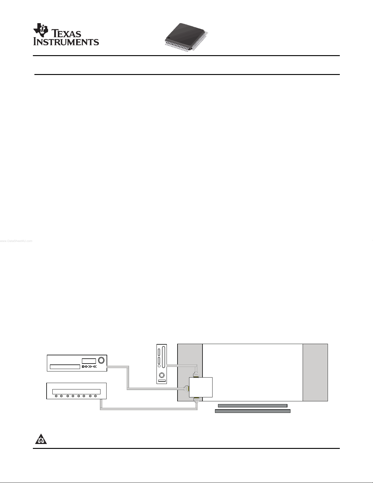
STB
DigitalTV
DVDPlayer
Game
Console
TMDS351
3-to-1
PHY SX
2.5 Gbps 3-TO-1 DVI/HDMI SWITCH
TMDS351
SLLS840 – MAY 2007
FEATURES
• Compatible with HDMI 1.3a
• Supports 2.5 Gbps Signaling Rate for 480i/p,
• HBM ESD Protection Exceeds 8 kV to TMDS
Inputs
• 3.3-V Fixed Supply to TMDS I/Os
720i/p, and 1080i/p Resolutions up to 12-Bit • 5-V Fixed Supply to HPD, DDC, and Source
Color Depth Selection Circuits
• Integrated Receiver Termination • 64-Pin TQFP Package
• Selectable Receiver Equalization to • ROHS Compatible and 260 ° C Reflow Rated
Accommodate to Different Input Cable
Lengths
• Intra-Pair Skew < 40 ps
• Inter-Pair Skew < 65 ps
APPLICATIONS
• Digital TV
• Digital Projector
DESCRIPTION
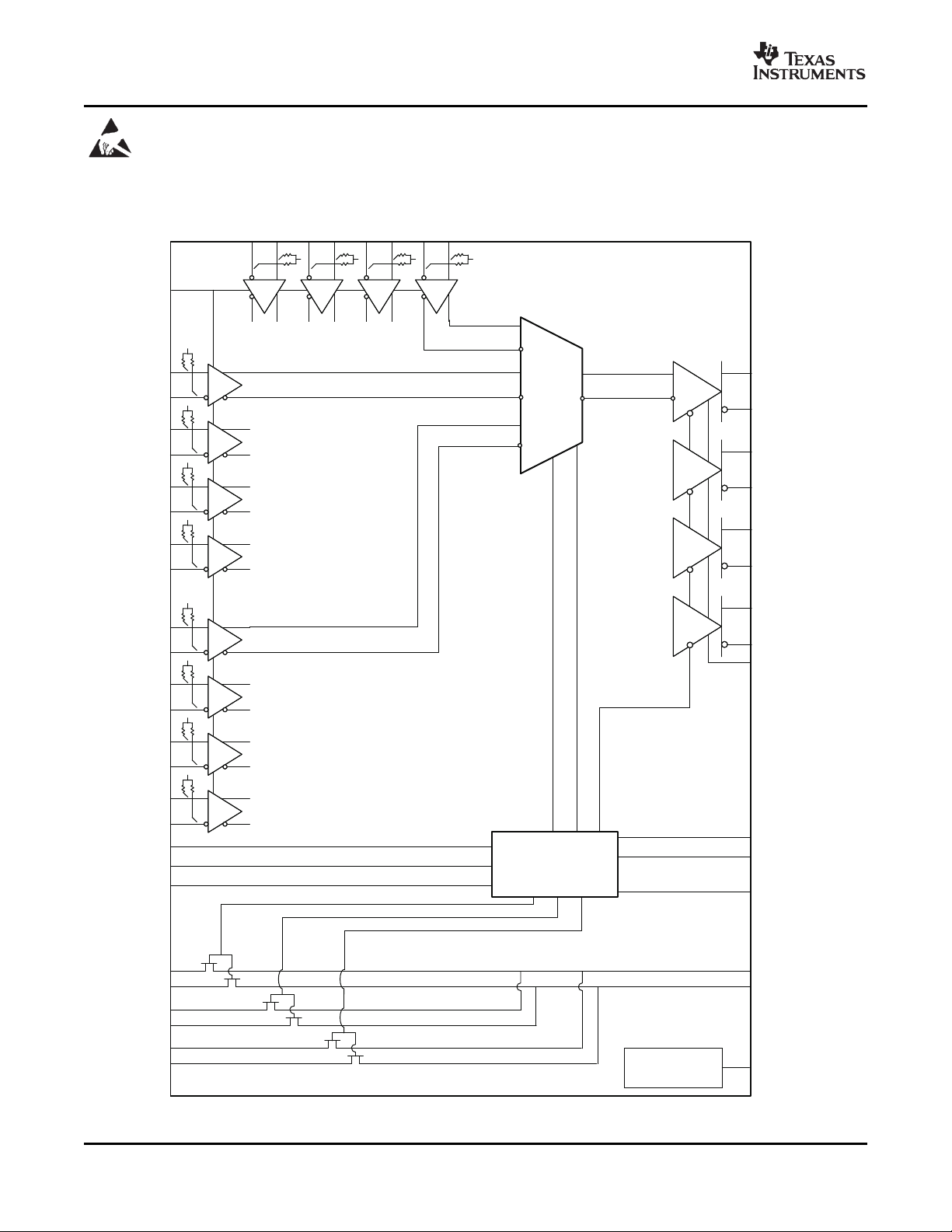
The TMDS351 is a 3-port digital video interface (DVI) or high-definition multimedia interface (HDMI) switch that
allows up to 3 DVI or HDMI ports to be switched to a single display terminal. Four TMDS channels, one hot plug
detector, and a digital display control (DDC) interface are supported on each port. Each TMDS channel supports
signaling rates up to 2.5 Gbps to allow 1080p resolution in 12-bit color depth.
When S1 is high and S2 is low, all input terminations are disconnected, TMDS inputs are high impedance with
standard TMDS terminations, all internal MOSFETs are turned off to disable the DDC links, and all HPD outputs
are connected to the HPD_SINK. This allows the initiation of the HDMI physical address discovery process.
Termination resistors (50- Ω ), pulled up to V
are not required. A precision resistor is connected externally from the VSADJ pin to ground for setting the
differential output voltage to be compliant with the TMDS standard.
The TMDS351 provides two levels of receiver input equalization for different ranges of cable lengths. Each
TMDS receiver owns frequency responsive equalization circuits. When EQ sets low, the receiver supports the
input connection in short range HDMI cables. When EQ sets high, the receiver supports the input connection in
long range HDMI cables. The TMDS351 supports power saving operation. When a system is under standby
mode and there is no digital audio/visual content from a connected source, the 3.3-V supply voltage, V
be powered off to minimize power consumption from the TMDS inputs, outputs, and internal switching circuits.
The HPD, DDC, and source selection circuits are powered up by the 5-V supply voltage, V
system hot plug detect response, the DDC link from the selected source to the sink under system standby
operation. The device is characterized for operation from 0 ° C to 70 ° C.
, are integrated at each TMDS receiver input. External terminations
CC
, to maintain the
DD
CC
, can
Please be aware that an important notice concerning availability, standard warranty, and use in critical applications of Texas
Instruments semiconductor products and disclaimers thereto appears at the end of this data sheet.
PRODUCTION DATA information is current as of publication date.
Products conform to specifications per the terms of the Texas
Instruments standard warranty. Production processing does not
necessarily include testing of all parameters.
Typical Application
Copyright © 2007, Texas Instruments Incorporated
www.ti.com
SCL_SINK
SDA_SINK
HPD_SINK
S1
S2
.
.
.
.
.
.
.
.
.
Control
Logic
Y4
Z4
VSADJ
TMDS
Driver
TMDS
Driver
TMDS
Driver
TMDS
Driver
EQ
V
DD
Vcc
R
INT
TMDS
Rx
R
INT
Vcc
R
INT
TMDS
Rx
R
INT
Vcc
R
INT
TMDS
Rx
R
INT
Vcc
R
INT
TMDS
Rx
R
INT
Vcc
R
INT
TMDS
Rx
R
INT
Vcc
R
INT
TMDS
Rx
R
INT
Vcc
R
INT
TMDS
Rx
R
INT
Vcc
R
INT
TMDS
Rx
R
INT
Vc c
R
INT
TMDS
Rx
R
INT
Vc c
R
INT
TMDS
Rx
R
INT
Vc c
R
INT
TMDS
Rx
R
INT
Vc c
R
INT
TMDS
Rx
R
INT
B11
A1
1
B12
A12
B13
A13
B14
A14
A24
B24
A23
B23
A22
B22
A21
B21
A34
B34
A33
B33
A32
B32
A31
B31
HPD1
HPD2
HPD3
SCL1
SDA1
SCL2
SDA2
SCL3
SDA3
Y3
Z3
Y1
Z1
Y2
Z2
HPD/DDC
PowerSupply
TMDS351
SLLS840 – MAY 2007
These devices have limited built-in ESD protection. The leads should be shorted together or the device placed in conductive foam
during storage or handling to prevent electrostatic damage to the MOS gates.
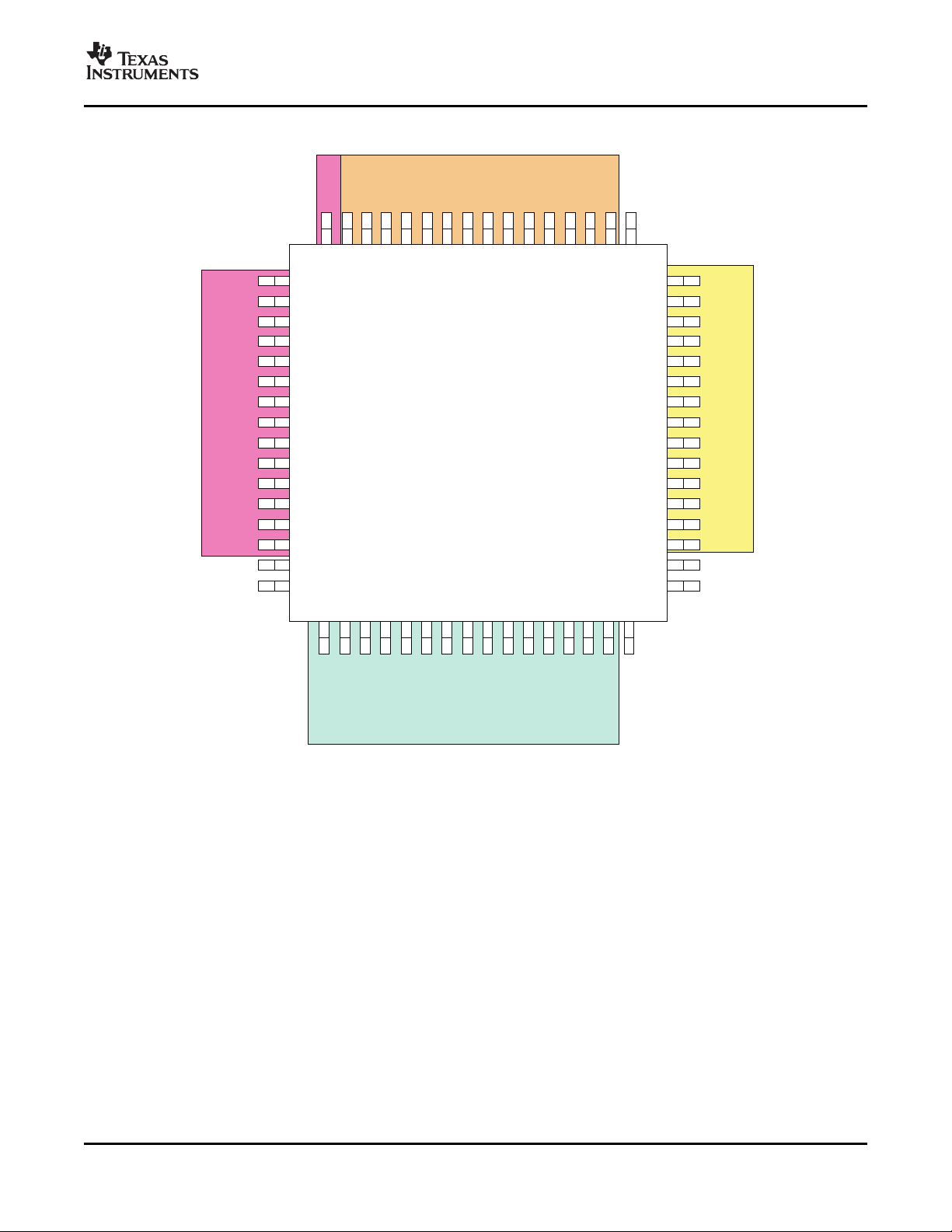
FUNCTIONAL BLOCK DIAGRAM
2
Submit Documentation Feedback
www.ti.com
1
2
3
4
5
6
7
8
9
10
11
12
13
14
15
16
TMDS351
64-pin TQFP
SDA3
SCL3
GND
B31
A31
Vcc
B32
A32
GND
B33
A33
Vcc
B34
A34
GND
VSADJ
17
18
19
20
21
22
23
24
25
26
27
28
29
30
31
32
Y4
Z4
Vcc
Y3
Z3
GND
Y2
Z2
Vcc
Y1
Z1
GND
SCL_SINK
SDA_SINK
HPD_SINK
S1
48
47
46
45
44
43
42
41
40
39
38
37
36
35
34
33
A14
B14
Vcc
A13
B13
GND
A12
B12
Vcc
A11
B11
SCL1
SDA1
HPD1
EQ
S2
64
63
62
61
60
59
58
57
56
55
54
53
52
51
50
49
HPD3
A24
B24
Vcc
A23
B23
GND
A22
B22
Vcc
A21
B21
SCL2
SDA2
HPD2
VDD
TMDS351
SLLS840 – MAY 2007
PFC PACKAGE
(TOP VIEW)
Submit Documentation Feedback
3

www.ti.com
TMDS351
SLLS840 – MAY 2007
TERMINAL FUNCTIONS
TERMINAL
NAME NO.
A11, A12, A13, A14 39, 42, 45, 48 I Source port 1 TMDS positive inputs
A21, A22, A23, A24 54, 57, 60, 63 I Source port 2 TMDS positive inputs
A31, A32, A33, A34 5, 8, 11, 14 I Source port 3 TMDS positive inputs
B11, B12, B13, B14 38, 41, 44, 47 I Source port 1 TMDS negative inputs
B21, B22, B23, B24 53, 56, 59, 62 I Source port 2 TMDS negative inputs
B31, B32, B33, B34 4, 7, 10, 13 I Source port 3 TMDS negative inputs
GND Ground
EQ 34 I EQ = Low – HDMI 1.3 compliant cable
HPD1 35 O Source port 1 hot plug detector output (status pin)
HPD2 50 O Source port 2 hot plug detector output (status pin)
HPD3 64 O Source port 3 hot plug detector output (status pin)
HPD_SINK 31 I Sink port hot plug detector input (status pin)
SCL1 37 I/O Source port 1 DDC I2C clock line
SCL2 52 I/O Source port 2 DDC I2C clock line
SCL3 2 I/O Source port 3 DDC I2C clock line
SCL_SINK 29 I/O Sink port DDC I2C clock line
SDA1 36 I/O Source port 1 DDC I2C data line
SDA2 51 I/O Source port 2 DDC I2C data line
SDA3 1 I/O Source port 3 DDC I2C data line
SDA_SINK 30 I/O Sink port DDC I2C data line
S1, S2 32. 33 I Source selector
V
CC
V
DD
VSADJ 16 I TMDS compliant voltage swing control (control pin)
Y1, Y2, Y3, Y4 26,23,20,17 O Sink port TMDS positive outputs
Z1, Z2, Z3, Z4 27,24,21,18 O Sink port TMDS negative outputs
3, 9, 15, 22, 28,
43, 58
6, 12, 19, 25, 40,
46, 55, 61
49 HPD/DDC Power supply
I/O DESCRIPTION
TMDS Input equalization selector (control pin)
EQ = High – 10m 28 AWG HDMI cable
Power supply
4
Submit Documentation Feedback

www.ti.com
Table 1. Source Selection Lookup
CONTROL PINS I/O SELECTED HOT PLUG DETECT STATUS
S1 S2 Y/Z HPD1 HPD2 HPD3
A1/B1 SCL1
H H HPD_SINK L L
H L L HPD_SINK L
L L L L HPD_SINK
L H None (Z) None (Z) HPD_SINK HPD_SINK HPD_SINK
(1) H: Logic high; L: Logic low; X: Don't care; Z: High impedance
Terminations of A2/B2 SDA1
and A3/B3 are
disconnected
A2/B2 SCL2
Terminations of A1/B1 SDA2
and A3/B3 are
disconnected
A3/B3 SCL3
Terminations of A1/B1 SDA3
and A2/B2 are
disconnected
All terminations are Are pulled HIGH by
disconnected external pull-up
SCL_SINK
SDA_SINK
termination
(1)
TMDS351
SLLS840 – MAY 2007
Submit Documentation Feedback
5
www.ti.com
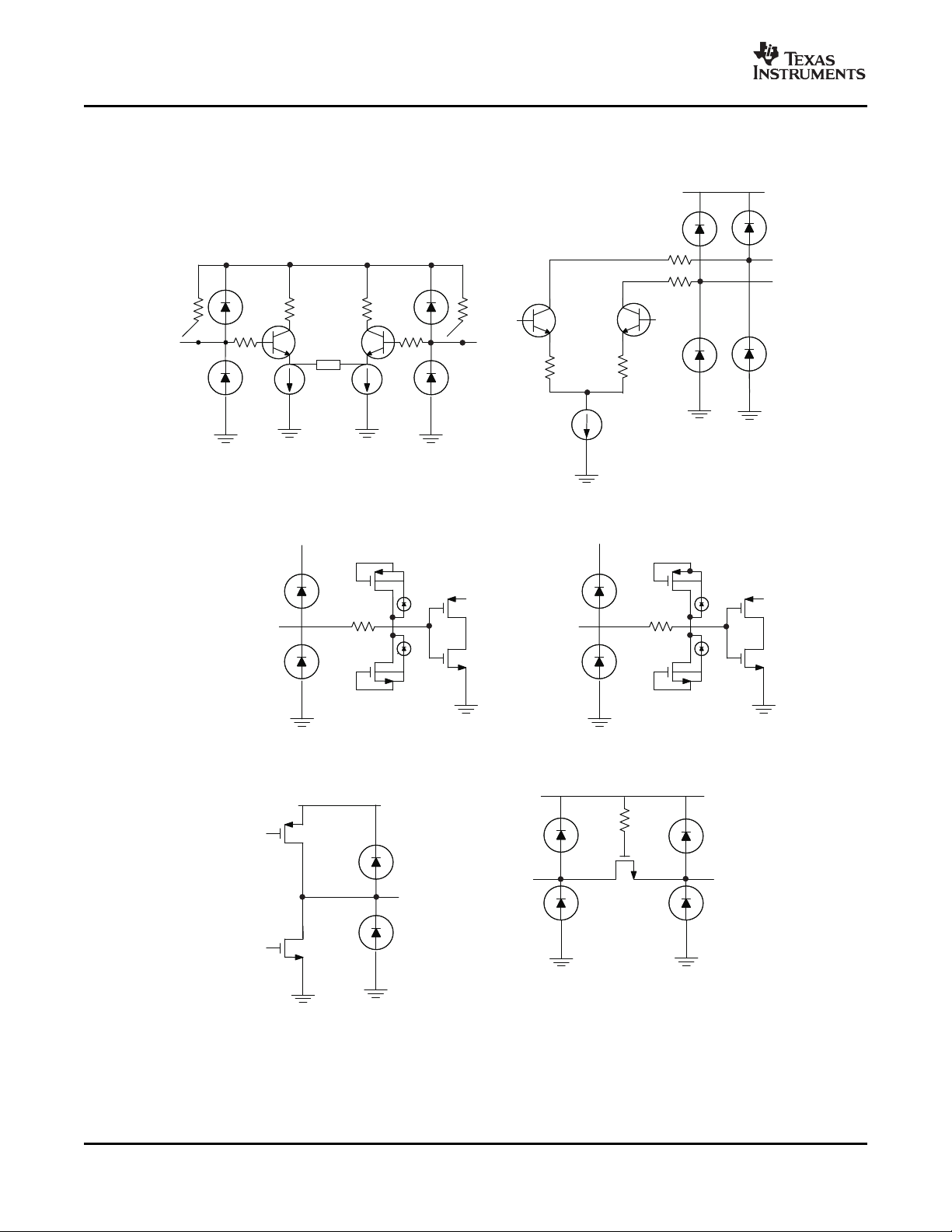
TMDSInputStage
A B
V
CC
50 W
Z
TMDSOutputStage
Y
10mA
StatusandSourceSelector
HPD_SINK
S1
S2
V
DD
ControlInputStage
EQ
V
CC
SCL/SCA
Source
DDCpassgate
HPDoutputstage
HPD1
HPD2
HPD3
V
DD
50 W
V
DD
SCL/SCA
Sink
V
CC
TMDS351
SLLS840 – MAY 2007
EQUIVALENT INPUT AND OUTPUT SCHEMATIC DIAGRAMS
6
Submit Documentation Feedback
www.ti.com
TMDS351
SLLS840 – MAY 2007
ORDERING INFORMATION
PART NUMBER PART MARKING PACKAGE
TMDS351PAG TMDS351 64-PIN TQFP
TMDS351PAGR TMDS351 64-PIN TQFP Tape/Reel
(1) For the most current package and ordering information, see the Package Option Addendum at the end of this document, or see the TI
web site at www.ti.com.
ABSOLUTE MAXIMUM RATINGS
over operating free-air temperature range (unless otherwise noted)
Supply voltage V
(2)
range
Voltage range Ym, Zm, VSADJ, EQ –0.5V to 4 V
Electrostatic
discharge
Continuous power dissipation
(1) Stresses beyond those listed under absolute maximum ratings may cause permanent damage to the device. These are stress ratings
only and functional operation of the device at these or any other conditions beyond those indicated under recommended operating
conditions is not implied. Exposure to absolute-maximum-rated conditions for extended periods may affect device reliability.
(2) All voltage values, except differential I/O bus voltages, are with respect to network ground terminal.
(3) n = 1, 2, 3; m = 1, 2, 3, 4
(4) Tested in accordance with JEDEC Standard 22, Test Method A114-B
(5) Tested in accordance with JEDEC Standard 22, Test Method C101-A
(6) Tested in accordance with JEDEC Standard 22, Test Method A115-A
CC
V
DD
(3)
Anm
, Bnm 2.5 V to 4 V
SCLn, SCL_SINK, SDAn, SDA_SINK, HPDn, HPD_SINK, S1, S2 –0.5 V to 6 V
Human body model
Charged-device model
Machine model
(4)
(5)
(all pins) ± 1500 V
(6)
(all pins) ± 200 V
(1)
Anm, Bnm ± 8000 V
All pins ± 4000 V
(1)
UNIT
–0.5 V to 4 V
–0.5 V to 6 V
See Dissipation Rating
Table
DISSIPATION RATINGS
PACKAGE TA≤ 25 ° C
64-TQFP PAG
PCB JEDEC DERATING FACTOR
STANDARD ABOVE TA= 25 ° C POWER RATING
Low-K 1111 mW 11.19 mW/ ° C 611 mW
High-K 1492 mW 14.92 820 mW
(1) This is the inverse of the junction-to-ambient thermal resistance when board-mounted and with no air flow.
(1)
THERMAL CHARACTERISTICS
over operating free-air temperature range (unless otherwise noted)
PARAMETER TEST CONDITIONS MIN TYP MAX
R
Junction-to-board thermal
θ JB
resistance
R
Junction- to-case thermal
θ JC
resistance
P
Device power dissipation Am/Bm(2:4) = 2.5-Gbps HDMI data pattern, 590 750 mW
D
Am/Bm(1) = 250-MHz clock
(1) The maximum rating is simulation under 3.6-V VCC, 5.5-V VDD, and 600 mV VID.
Submit Documentation Feedback
VIH= VCC, VIL= V
- 0.6 V, RT= 50 Ω , AV
CC
= 3.3V,
CC
TA= 70 ° C
(1)
33.4 ° C/W
15.6 ° C/W
UNIT
7
www.ti.com
TMDS351
SLLS840 – MAY 2007
RECOMMENDED OPERATING CONDITIONS
V
CC
V
DD
T
A
TMDS DIFFERENTIAL PINS
V
IC
V
ID
R
VSADJ
AV
CC
R
T
CONTROL PINS
V
IH
V
IL
DDC I/O PINS
V
I(DDC)
STATUS and SOURCE SELECTOR PINS
V
IH
V
IL
Supply voltage 3 3.3 3.6 V
Standby supply voltage 4.5 5 5.5 V
Operating free-air temperature 0 70 ° C
Input common mode voltage VCC–0.4 VCC+0.01 V
Receiver peak-to-peak differential input voltage 150 1560 mVp-p
Resistor for TMDS compliant voltage swing range 3.66 4.02 4.47 k Ω
TMDS output termination voltage, see Figure 1 3 3.3 3.6 V
Termination resistance, see Figure 1 45 50 55 Ω
Signaling rate 0 2.5 Gbps
LVTTL High-level input voltage 2 V
LVTTL Low-level input voltage GND 0.8 V
DDC Input voltage GND V
LVTTL High-level input voltage 2 V
LVTTL Low-level input voltage GND 0.8 V
MIN NOM MAX UNIT
V
CC
V
DD
V
DD
ELECTRICAL CHARACTERISTICS
over recommended operating conditions (unless otherwise noted)
PARAMETER TEST CONDITIONS MIN TYP
VIH= VCC, VIL= VCC– 0.6 V, S1/S2 =
RT= 50 Ω , AV
I
CC
I
DD
Supply current mA
Power supply current, 5-V 2 5 mA
TMDS DIFFERENTIAL PINS
V
OH
V
OL
V
swing
V
OD(O)
V
OD(U)
∆ V
I
(OS)
V
I(open)
R
Single-ended high-level output voltage AV
Single-ended low-level output voltage AV
Single-ended output swing voltage 400 600 mV
Overshoot of output differential voltage 15% 2 × V
Undershoot of output differential voltage 25% 2 × V
Change in steady-state common-mode
OC(SS)
output voltage between logic states
Short circuit output current See Figure 3 -12 12 mA
Single-ended input voltage under high
impedance input or open input
Input termination resistance VIN= 2.9 V 45 50 55 Ω
INT
CONTROL PINS
I
IH
I
IL
High-level digital input current
Low-level digital input current
DDC I/O PINS
I
lkg
C
Input leakage current VI= 0.1 VDDto 0.9 VDDto isolated DDC inputs -10 10 µA
Input/output capacitance V
IO
(2)
(2)
Am/Bm(2:4) = 2.5 Gbps HDMI data Low/High,
pattern High/High
Am/Bm(1) = 250 MHz clock
VIH= VCC, VIL= VCC– 0.6 V,
RT= 50 Ω , AV
Am/Bm(2:4) = 2.5 Gbps HDMI data pattern
Am/Bm(1) = 250 MHz clock
See Figure 2 , AV
RT= 50 Ω
II= 10 µA VCC–10 VCC+10 mV
VIH= 2 V or V
VIL= GND or 0.8 V -10 10 µA
= 1 V, 100 kHz 10 pF
I(pp)
= 3.3 V Low/Low,
CC
= 3.3 V
CC
= 3.3 V,
CC
CC
S1/S2 =
High/Low
(1)
176 200
8 20
–10 AV
CC
–600 AV
CC
CC
-10 10 µA
MAX UNIT
+10 mV
CC
–400 mV
swing
swing
5 mV
(1) All typical values are at 25 ° C and with a 3.3-V supply.
(2) IIHand IILspecifications are not applicable to the VSADJ pin.
8
Submit Documentation Feedback

www.ti.com
ELECTRICAL CHARACTERISTICS (continued)
over recommended operating conditions (unless otherwise noted)
PARAMETER TEST CONDITIONS MIN TYP
R
V
PASS
STATUS AND SOURCE SELECTOR PINS
I
IH
I
IL
V
OH
V
OL
Switch resistance IO= 3 mA, VO= 0.4 V 27 40 Ω
ON
Switch output voltage VI= 5 V, IO= 100 µA 1.9 3.6 V
High-level digital input current VIH= 2 V or V
Low-level digital input current VIL= GND or 0.8 V -10 10 µA
TTL High-level output voltage IOH= –100 µ A 2.4 V
TTL Low-level output voltage IOL= 100 µ A GND 0.4 V
TMDS351
SLLS840 – MAY 2007
(1)
DD
-10 10 µA
MAX UNIT
V
DD
SWITCHING CHARACTERISTICS
(1)
over recommended operating conditions (unless otherwise noted)
PARAMETER TEST CONDITIONS MIN TYP
TMDS DIFFERENTIAL PINS (Y/Z)
t
PLH
t
PHL
t
r
t
f
t
sk(p)
t
sk(D)
t
sk(o)
t
sk(pp)
t
jit(pp)
t
jit(pp)
t
SX
t
en
t
dis
t
pd(DDC)
t
sx(DDC)
t
pd(HPD)
t
sx(HPD)
Propagation delay time, low-to-high-level output 400 650 900 ps
Propagation delay time, high-to-low-level output 400 650 900 ps
Differential output signal rise time (20% - 80%) 60 80 140 ps
Differential output signal fall time (20% - 80%) 60 80 140 ps
Pulse skew (|t
PHL
(3)
– t
|)
PLH
Intra-pair differential skew, see Figure 4 20 40 ps
Inter-pair channel-to-channel output skew
Part-to-part skew
(5)
(4)
Peak-to-peak output jitter from Yj/Zj(1) residual jitter See Figure 5 , 8 20 ps
Peak-to-peak output jitter from Yj/Zj(2:4) residual jitter 60 80 ps
Select to switch output 50 70 ns
Enable time 170 250 ns
Disable time 9 15 ns
Propagation delay from SCLn to SCL_SINK or SDAn to
SDA_SINK or SDA_SINK to SDAn
Switch time from SCLn to SCL_SINK 8 15 ns
Propagation delay (from HPD_SINK to the active port of HPD) 14 20 ns
Switch time from port select to the latest valid status of HPD 33 50 ns
See Figure 2 , AV
RT= 50 Ω , PRE = 0 V
= 3.3 V,
CC
Am/Bm(1) = 250 MHz clock,
Am/Bm(2:4) = 2.5 Gbps HDMI pattern
See Figure 6 ,
10-mA Current source to the input
See Figure 7 , CL= 10 pF
(2)
MAX UNIT
6 20 ps
30 65 ps
510 ps
8 15 ns
(1) Measurements are made with the Agilent 81250 ParBert System with a N4872A generator (600 fs t
analyzer.
JIT(CLK)
(2) All typical values are at 25 ° C and with a 3.3-V supply.
(3) t
(4) t
(5) t
is the magnitude of the time difference between t
sk(p)
is the magnitude of the difference in propagation delay times between any specified terminals of a sink-port bank when inputs of
sk(o)
the active source port are tied together.
is the magnitude of the difference in propagation delay times between any specified terminals of two devices when both devices
sk(pp)
operate with the same source, the same supply voltages, at the same temperature, and have identical packages and test circuits.
and t
PLH
of a specified terminal.
PHL
Submit Documentation Feedback
, 13 ps t
) and a N4873A
JIT(pp)
9

www.ti.com
TMDS
Driver
AVcc
R
T
R
T
TMDS
Receiver
ZO = R
T
ZO = R
T
V
OC(SS)
V
OC
t
PHL
t
PLH
100%
0V Differential
0%
80%
20%
t
f
t
r
V
ID
0.4 V
0 V
−0.4 V
V
OD(O)
V
OD(U)
V
OD(pp)
V
ID
V
ID(pp)
Vcc
R
INT
R
INT
TMDS
Receiver
TMDS
Driver
Y
Z
A
B
AVcc
R
T
R
T
V
ID
V
B
V
A
V
Y
V
Z
C
L
0.5 pF
V
A
V
B
Vcc
Vcc−0.4 V
VYV
Z
swing
= −
V
V
ID
= −
V V
BA
n
DC Coupled
Vcc+0.2 V
Vcc−0.2 V
AC Coupled
swing
V
TMDS351
SLLS840 – MAY 2007
PARAMETER MEASUREMENT INFORMATION
Figure 1. Termination for TMDS Output Driver
NOTE: All input pulses are supplied by a generator having the following characteristics: tror tf< 100 ps, 100 MHz from
Agilent 81250. C
equipment provides a bandwidth of 20 GHz minimum.
includes instrumentation and fixture capacitance within 0.06 m of the D.U.T. Measurement
L
Figure 2. Timing Test Circuit and Definitions
10
Submit Documentation Feedback

www.ti.com
TMDS
Driver
0 V or 3.6 V
50 W
50 W
_
+
I
OS
50%
V
OL
t
sk(D)
V
Y
V
Z
V
OH
Data +
Data -
Clk+
Clk-
Video Patterm
Generator
1000 mVpp
Differential
Coax
Coax
Coax
Coax
Coax
Coax
Coax
Coax
<2" 50!
Transmission Line
TMDS351
RX
+
EQ
M
U
X
OUT
RX
+
EQ
M
U
X
OUT
<2" 50!
Transmission Line
<2" 50!
Transmission Line
<2" 50!
Transmission Line
SMA
SMA
SMA
SMA
SMA
SMA
SMA
SMA
AVcc
RTR
T
AVcc
RTR
T
Jitter Test
Instrument
Jitter Test
Instrument
TP3
TP2TP1
HDMI Cables
PARAMETER MEASUREMENT INFORMATION (continued)
Figure 3. Short Circuit Output Current Test Circuit
Figure 4. Definition of Intra-Pair Differential Skew
TMDS351
SLLS840 – MAY 2007
A. HDMI 1.3 compliant cable when EQ = Low, and 10m 28AWG input cable when EQ = High.
B. All jitters are measured in BER of 10
-9
C. The residual jitter reflects the total jitter measured at the output of the DUT, TP3, subtract the total jitter from the
signal generator, TP1
Figure 5. Jitter Test Circuit
Submit Documentation Feedback
11

www.ti.com
S1
Clocking
S2
Input-1
keptHIGH
Input-2
kept
t
SX
A
B
A
B
Y
Z
Output
t
en
t
dis
Hi-Z
75mV
Input-3
keptLOW
A
B
VDD
2
VDD
0V
-75mV
75mV
-75mV
t
SX
HPD1
HPD2
S1
0.4 V
2.4 V
0 V
SDA_SINK
SDA1
SDA2
SDA3
S2
VDD
2
VDD
2
HPD3
0V
VDD
VDD
1.5V
1.5V
VDD
2
HPD_SINK
t
pd(HPD)
t
pd(HPD)
t
sx(HPD)
t
sx(DDC)
t
pd(DDC)
t
pd(DDC)
TMDS351
SLLS840 – MAY 2007
PARAMETER MEASUREMENT INFORMATION (continued)
Figure 6. TMDS Outputs Control Timing Definitions
Figure 7. DDC and HPD Timing Definitions
12
Submit Documentation Feedback

www.ti.com
0
50
100
150
200
250 450 650 850 1050 1250 1450 1650 1850 2450
SignalRate-Mbps
I -SupplyCurrent-mA
CC
S1=S2=HIGH
S1=HIGHS2=LOW
I
DD
V = AV =3.3V,T =25°C,
TP1V =1200mV ,R =4.02k ,
Am/Bm(2:4)HDMIDatapattern,250Mbps-2.5Gbps
Am/Bm(1)Clock,25MHz-250MHz
CC CC A
ID(PP) PP
VSADJ
W
0
50
100
150
200
0 10 20 30 40 50 60 70
T -Free AirTemperature- CA°
I -SupplyCurrent-mA
CC
S1=S2=HIGH
S1=HIGHS2=LOW
I
DD
V = AV =3.3V,
V =1200mV ,R =4.02k ,
Am/Bm(2:4) HDMIDatapattern,
Am/Bm(1) Clock
CC CC
ID(PP) PP
VSADJ
W
2.5-Gbps
250-MHz
0
1
2
3
4
5
75 95 115 148.5 185 225
f-Frequency-MHz
Peak-to-PeakJitter-%Tbit
EQ=LOW3m30 AWG
EQ=LOW5m28 AWG
EQ=HIGH10m28 AWG
EQ=HIGH15m26 AWG
SeeNote A
0
5
10
15
20
750 950 1150 1485 1850 2250
SignalRate-Mbps
Peak-to-PeakJitter-%Tbit
EQ=HIGH10m28 AWG
EQ=LOW3m30 AWG
EQ=LOW
5m28 AWG
EQ=HIGH
15m26 AWG
SeeNote A
TMDS351
SLLS840 – MAY 2007
TYPICAL CHARACTERISTICS
SUPPLY CURRENT SUPPLY CURRENT
vs vs
SIGNAL RATE FREE-AIR TEMPERATURE
Figure 8. Figure 9.
RESIDUAL PEAK-TO-PEAK JITTER RESIDUAL PEAK-TO-PEAK JITTER
(Data Channels) (Clock Channel)
vs vs
SIGNAL RATE FREQUENCY
A. Channels 2, 3, 4, V
25 ° C, R
VSADJ
= 4.02 k Ω , See Figure 6 R
= AV
CC
Figure 10. Figure 11.
= 3.3 V, TA= A. Channel 1, V
CC
CC
= 4.02 k Ω , See Figure 6
VSADJ
= AV
Submit Documentation Feedback
= 3.3 V, TA= 25 ° C,
CC
13

www.ti.com
0
2
4
6
8
10
12
14
16
18
20
1.5m
30AWG
3m30
AWG5m28AWG
10m
28AWG
15m
26AWG
EQ=Low
Peak-to-PeakJitter-%Tbit
Cable
EQ=High
SeeNote A
0
5
10
15
20
1.5m
30AWG
3m30
AWG
5m 10m
28AWG
15m
26AWG
EQ=Low
EQ=High
Peak-to-PeakJitter-%Tbit
28AWG
Cable
SeeNote A
TMDS351
SLLS840 – MAY 2007
TYPICAL CHARACTERISTICS (continued)
RESIDUAL PEAK-TO-PEAK JITTER RESIDUAL PEAK-TO-PEAK JITTER
(Data Channel) (Data Channel)
vs vs
CABLE CABLE
A. 1080p 10-Bit, V
25 ° C, R
VSADJ
= AV
CC
= 3.3 V, TA= A. 1080p 12-Bit, V
CC
= 4.02 k Ω , See Figure 6 , 25 ° C, R
VSADJ
Clock Channel = 185.6 MHz, Data Channel Clock Channel = 222.8 MHz, Data Channel
= 1.856 Gbps = 2.228 Gbps
Figure 12. Figure 13.
= AV
CC
= 3.3 V, TA=
CC
= 4.02 k Ω , See Figure 6 ,
14
Submit Documentation Feedback

www.ti.com
-13
-12
-11
-10
-9
-8
-7
-6
-5
-4
-3
-2
-1
0
0 250 500 750 1000 1250 1500 1750 2000
f-Frequency-MHz
Loss-dB
spec
EQ=Low
3m30 AWGcable
TMDS351
SLLS840 – MAY 2007
APPLICATION INFORMATION
Supply Voltage
The TMDS351 is powered up with two different power sources. One is 3.3-V V
other is 5-V V
for HPD, DDC, and most of the control logic. It is recommended to provide the same 3.3-V
DD
power source to the TMDS circuitry of the TMDS351 and its output termination voltage. This minimizes the
leakage current from the ESD protection circuitry. When the digital television (DTV) is in standby mode
operation, the same common 3.3-V power source can be turned on or off. Either way will minimize the leakage
current in the device, and in the receiver connected at the output where the termination is integrated.
TMDS Inputs
Selectable frequency response equalization circuitries are provided to all twelve differential input to support short
range and long range cable connections. The frequency response compensation curves and target cable losses
are shown in Figure 14 and Figure 15 .
for the TMDS circuitry, and the
CC
Figure 14. Frequency Response Compensation Curve at EQ = L
Submit Documentation Feedback
15

www.ti.com
-20
-18
-16
-14
-12
-10
-8
-6
-4
-2
0
0 250 500 750 1000 1250 1500 1750 2000
f-Frequency-MHz
Loss-dB
spec
10mcable
EQ=High
V
CC
R
INT
R
INT
TMDS
Receiver
TMDS
Driver
R
T
R
T
Y
Z
A
B
AV
CC
TMDS351
SLLS840 – MAY 2007
APPLICATION INFORMATION (continued)
Figure 15. Frequency Response Compensation Curve at EQ = H
Internal termination circuitry which can be switched on or off, provides 50- Ω resistance to each differential input
pin when a port is selected. External terminations are not required. When the termination is switched on, current
will flow to the TMDS driver. When a port is not selected, the termination is open. This stops supply current
flowing from the input pins of the un-selected ports. This switchable termination provides the connected HDMI
source another method of determining the sink port status, and whether it is selected or not selected, without
referring to the HPD pin status.
TMDS Input Fail-Safe
The TMDS input does not incorporate a fail-safe circuit. To implement fail-safe, the input can be externally
biased to prevent output oscillation. One pin can be pulled high to V
resistor as shown in Figure 16 .
with the other grounded through a 1-k Ω
CC
16
Figure 16. TMDS Input Fail-Safe Recommendation
Submit Documentation Feedback

www.ti.com
R
upSource
V
DDSource
Source Sink
Ron
SCL_SINK
SDA_SINK
SCL
SDA
Driver(Source)
I
to-Sink
I
to-Source
V
DDSink
R
upSink
V
CCRx
R
upRx
Driver(Sink)
Ito * Sink +
Vdd* V
ol(Sink)max
R
upSource
ø R
upSink
lto * Sink +
V
dd
R
upSource
ø R
upSink
V
ith(Source)min
u lto * Sink Ron) V
ol(Sink)max
R
upSink
w
Vdd Ron R
upSource
(V
ith(Source)min
* V
ol(Sink)max
) R
upSource
* Vdd Ron
TMDS351
SLLS840 – MAY 2007
APPLICATION INFORMATION (continued)
TMDS Outputs
A 10% precision resistor, 4.02-k Ω , is recommended to control the output swing to the HDMI compliant 400 mV
to 600 mV range (500 mV typical). The TMDS outputs are high impedance under standby mode operation, S1 =
H and S2 = L.
HPD Pins
The HPD circuits are powered by the 5-V supply. They provide 5-V TTL output signals to the SOURCE with a
typical 1-k Ω output resistance. An external 1-k Ω resistor is not needed here. The HPD output of the selected
source port follows the logic level of the HPD_SINK input. Unselected HPD outputs are kept low. When the
device is in standby mode, all HPD outputs follow HPD_SINK. A 1-k Ω resistor to ground keeps all HPD outputs
low in standby mode if a fixed low state is preferred.
DDC Channels
The DDC circuits (SDA, SCL) are powered by a 5-V supply. The I/O pins can connect to the 5-V termination
voltages directly. A 47-k Ω pull-up resistor to the 5 V is recommended on the SCL1, SCL2, and SCL3 pins. There
is no pull-up resistor on the SDA pins. The pull-up resistor can be replaced with a different value.
Figure 17. Simplified Electrical Circuit Model for DDC Channel
In Figure 17 , when the Driver (Sink) pulls the bus low, the highest voltage level is V
through the pass-gate resistor can be presented as:
where the V
ddsource
To simplify the equation, V
= V
ddsink
ol(Sink)max
The voltage at the input of the SINK is Ito - Sink × Ron + V
input low threshold voltage of the Driver (Source), V
By combining equations (2) and (3), the minimum pull-up resistor at the Sink input is:
= V
dd
is set equal to 0 V to reach equation (2):
ol(Sink)max
to keep the bus in correct interoperations.
Submit Documentation Feedback
ith(Source)min
ol(Sink)max
, which should be lower than the minimum
. The current flow
(1)
(2)
(3)
(4)
17

www.ti.com
R
upRx
w
V
ccRx
Ron
(V
ith(Sink)min
* V
ol(Source)max
)
TMDS351
SLLS840 – MAY 2007
APPLICATION INFORMATION (continued)
Applying the same methodology to calculate the pull-up resistor at the input of the Driver (Sink), the minimum
pull-up resistor is:
The data sheet V
connection. Resistors pulling up to 3.3 V on SCL_SINK and SDA_SINK ensure the high level does not exceed
the 3.3-V termination voltage.
Layout Considerations
The high-speed differential TMDS inputs are the most critical paths for the TMDS351. There are several
considerations to minimize discontinuities on these transmission lines between the connectors and the device:
• Maintain 100- Ω differential transmission line impedance into and out of the TMDS351
• Keep an uninterrupted ground plane beneath the high-speed I/Os
• Keep the ground-path vias to the device as close as possible to allow the shortest return current path
• Keep the trace lengths of the TMDS signals between connector and device as short as possible
Using the TMDS351 in Systems with Different CEC Link Requirements
The TMDS351 supports a DTV with up to three HDMI inputs when used in conjunction with a signal-port HDMI
receiver or four HDMI inputs when used in conjunction with a dual-port HDMI receiver. Figure 18 and Figure 19
show simplified application block diagrams for the TMDS351 in different DTVs with different consumer electronic
control (CEC) requirements. The CEC is an optional feature of the HDMI interface for centralizing and
simplifying user control instructions from multiple audio/video products in an inter-connected system, even when
all the audio/video products are from different manufacturers. This feature minimizes the number of remote
controls in a system, as well as reducing the number of times buttons need to be pressed.
specification ensures the maximum output voltage is clamped at 3.6 V to support a 3.3-V
PASS
(5)
A DTV Supporting a Passive CEC Link
In Figure 18 , the DTV does not have the capability of handling CEC signals, but allows CEC signals to pass over
the CEC bus. The source selection is done by the control command of the DTV. The user cannot force the
command from any audio/video product on the CEC bus. The selected source reads the E-EDID data after
receiving an asserted HPD signal. The micro-controller loads different CEC physical addresses while changing
the source by means of the S1 and S2 pins.
E-EDID Reading Configurations in Standby Mode
When the DTV system is in standby mode, the sources will not read the E-EDID memory because the 1-k Ω
pull-down resistor keeping the HPD_SINK input at logic low forces all HPD pins to output logic low to all
sources. The source will not read the E-EDID data with a low on HPD signal. However, if reading the E-EDID
data in the system standby mode is preferred, then TMDS351 can still support this need.
The recommended configuration sequences are:
1. Apply the same 3.3-V power to the V
2. Turn off V
, and keep V
CC
on. The TMDS circuit is off, but the HPD, the DDC and the source selection
DD
circuits are active.
3. Set S1 and S2 to select the source port which is allowed to read the E-EDID memory.
Please note if the source has a time-out limitation between the 5 V and the HPD signals, the above configuration
is not applicable. Uses individual EEPROMs assigned for each input port, see Figure 19 . The solution uses
E-EDID data to be readable during system power off or standby mode operations.
of TMDS351 and the TMDS line termination at the HDMI receiver
CC
18
Submit Documentation Feedback

www.ti.com
SINK
HDMIRX
DDC_SDA
DDC_SCL
5V
5V
5V
47kW
47kW
47kW
3.3V
4.7kW 4.7kW
CEC
CEC
CEC
4.02 k
W 10%
E-EDID
E-EDID
E-EDID
mController
HPD1
SDA1
SCL1
HPD2
SDA2
SCL2
HPD3
SDA3
SCL3
EQ
S1
S2
HPD_SINK
SDA_SINK
SCL_SINK
Y1/Z1
Y2/Z2
Y3/Z3
Y4/Z4
VSADJ
GND
SDA SCL
CEC
LOGIC
CEC
PHY
1k
W
1kW
1k W
HPD
5V
SDA
SCL
CEC
CLK
D0
D1
D2
HPD
5V
SDA
SCL
CEC
CLK
D0
D1
D2
HPD
5V
SDA
SCL
CEC
CLK
D0
D1
D2
HPD
5V
SDA
SCL
CEC
CLK
D0
D1
D2
HPD
5V
SDA
SCL
CEC
CLK
D0
D1
D2
HPD
5V
SDA
SCL
CEC
CLK
D0
D1
D2
SOURCE1
With ACCoupled
HDMIOutput
SOURCE2
WithDCCoupled
HDMIOutput
SOURCE3
inGeneral
HDMIOutput
A11/B11
A12/B12
A13/B13
A14/B14
A21/B21
A22/B22
A23/B23
A24/B24
A31/B31
A32/B32
A33/B33
A34/B34
VDD
(5V)
VCC
(3.3V)
Y1/Z1
Y2/Z2
Y3/Z3
Y4/Z4
APPLICATION INFORMATION (continued)
TMDS351
SLLS840 – MAY 2007
A DTV Supporting an Active CEC Link
In Figure 19 , the CEC PHY and CEC LOGIC functions are added. The DTV can initiate and/or react to CEC
signals from its remote control or other audio/video products on the same CEC bus. All sources must have their
own CEC physical address to support the full functionality of the CEC link.
A source reads its CEC physical address stored its E-EDID memory after receiving a logic-high from the HPD
feedback. When HPD is high, the sink-assigned CEC physical address should be maintained. Otherwise, when
HPD is low the source sets CEC physical address value to (F.F.F.F).
Case 1 – AC Coupled Source (See Figure 19 , Port 1)
When the source TMDS lines are AC coupled or when the source cannot detect the TMDS termination provided
in the connected sink, the indication of the source selection can only come from the HPD signal. The TMDS351
HPD1 pin should be applied directly as the HPD signal back to the source.
Case 2 – DC Coupled Source (See Figure 19 , Port 2)
When the source TMDS lines are DC coupled, there are two methods to inform the source that it is the active
source to the sink. One is checking the HPD signal from the sink, and the other is checking the termination
condition in the sink.
In a full CEC operation mode, the HPD signal is set high whether the port is selected or not. The source loads
and maintains the CEC physical address when HPD is high. As soon as HPD goes low, the source loses the
CEC physical address. To keep the CEC physical address to the source, the HPD signal is looping back from
Figure 18. Three-Port HDMI Enabled DTV with TMDS351 – CEC Commands Passing Through
Submit Documentation Feedback
19

www.ti.com
HPD1
SDA1
SCL1
HPD2
SDA2
SCL2
HPD3
SDA3
SCL3
EQ
S1
S2
HPD_SINK
SDA_SINK
SCL_SINK
Y1/Z1
Y2/Z2
Y3/Z3
Y4/Z4
VSADJ
E-EDID
HDMIRX
DDC_SDA
DDC_SCL
5V
5V
5V
47kW
47kW
47kW
mController
3.3V
4.7kW 4.7kW
CEC
CEC
CEC
4.02kW 10%
GND
1kW
HPD
5V
SDA
SCL
CEC
CLK
D 0
HPD
5V
SDA
SCL
CEC
CLK
D0
D1
D2
HPD
5V
SDA
SCL
CEC
CLK
D0
D1
D2
SINK
HPD
5V
SDA
SCL
CEC
CLK
D0
D1
D2
SOURCE1
HPD
5V
SDA
SCL
CEC
CLK
D0
1D
D2
D1
D2
SOURCE2
HPD
5V
SDA
SCL
CEC
CLK
D0
D1
D2
SOURCE3
A11/B11
A12/B12
A13/B13
A14/B14
VDD
(5V)
VCC
(3.3V)
A21/B21
A22/B22
A23/B23
A24/B24
A31/B31
A32/B32
A33/B33
A34/B34
Y1/Z1
Y2/Z2
Y3/Z3
Y4/Z4
TMDS351
SLLS840 – MAY 2007
APPLICATION INFORMATION (continued)
the source provided 5-V signal through a 1-k Ω pull-up resistor in the sink. This method is acceptable in
application where the HDMI transmitter can detect the receiver termination by current sensing, and the receiver
has switchable termination on the TMDS inputs. The internal termination resistors are connected to the
termination voltage when the port is selected, or they are disconnected when the port is not selected. The
TMDS351 features switchable termination on the TMDS inputs.
Case 3 – External Logic Control for HPD (See Figure 19 , Port 3)
When the HDMI transmitter does not have the capability of detecting the receiver termination, using the HPD
signal as a reference for sensing port selections is the only possible method. External control logic for switching
the connections of the HPD signals between the HPD pins of the TMDS351 and the 5-V signal from the source
provides a good solution.
E-EDID Reading Configurations in Standby Mode
When the TMDS351 is in standby mode operation, S1 = H and S2 = L, all sources can read their E-EDID
memories simultaneously with all HPD pins following HPD_SINK in logic-high. HPD_SINK input low will prevent
E-EDID reading in standby mode operation.
20
Figure 19. Three-Port HDMI Enabled DTV with TMDS351 – CEC Commands Active
Submit Documentation Feedback

PACKAGE OPTION ADDENDUM
www.ti.com
29-May-2007
PACKAGING INFORMATION
Orderable Device Status
(1)
Package
Type
Package
Drawing
Pins Package
Qty
Eco Plan
TMDS351PAG ACTIVE TQFP PAG 64 160 Green (RoHS &
no Sb/Br)
TMDS351PAGR ACTIVE TQFP PAG 64 1500 Green (RoHS &
no Sb/Br)
(1)
The marketing status values are defined as follows:
ACTIVE: Product device recommended for new designs.
LIFEBUY: TI has announced that the device will bediscontinued,and a lifetime-buy period is in effect.
NRND: Not recommended for new designs. Device is in production to support existing customers, but TI does not recommend using this part in
a new design.
PREVIEW: Device has been announced but is not in production. Samples may or may not be available.
OBSOLETE: TI has discontinued the production of the device.
(2)
Eco Plan - The planned eco-friendly classification: Pb-Free (RoHS), Pb-Free (RoHS Exempt), or Green (RoHS & no Sb/Br) - please check
http://www.ti.com/productcontent for the latest availability information and additional product content details.
TBD: The Pb-Free/Green conversion plan has not been defined.
Pb-Free (RoHS): TI's terms "Lead-Free" or "Pb-Free" mean semiconductor products that are compatible with the current RoHS requirements
for all 6 substances, including the requirement that lead not exceed 0.1% by weight in homogeneous materials. Where designed to be soldered
at high temperatures, TI Pb-Free products are suitable for use in specified lead-free processes.
Pb-Free (RoHS Exempt): This component has a RoHS exemption for either 1) lead-based flip-chip solder bumps used between the die and
package, or 2) lead-based die adhesive used between the die and leadframe. The component is otherwise considered Pb-Free (RoHS
compatible) as defined above.
Green (RoHS & no Sb/Br): TI defines "Green" to mean Pb-Free (RoHS compatible), and free of Bromine (Br) and Antimony (Sb) based flame
retardants (Br or Sb do not exceed 0.1% by weight in homogeneous material)
(2)
Lead/Ball Finish MSL Peak Temp
CU NIPDAU Level-4-260C-72 HR
CU NIPDAU Level-4-260C-72 HR
(3)
(3)
MSL, Peak Temp. -- The Moisture Sensitivity Level rating according to the JEDEC industry standard classifications, and peak solder
temperature.
Important Information and Disclaimer:The information provided on this page represents TI's knowledge and belief as of the date that it is
provided. TI bases its knowledge and belief on information provided by third parties, and makes no representation or warranty as to the
accuracy of such information. Efforts are underway to better integrate information from third parties. TI has taken and continues to take
reasonable steps to provide representative and accurate information but may not have conducted destructive testing or chemical analysis on
incoming materials and chemicals. TI and TI suppliers consider certain information to be proprietary, and thus CAS numbers and other limited
information may not be available for release.
In no event shall TI's liability arising out of such information exceed the total purchase price of the TI part(s) at issue in this document sold by TI
to Customer on an annual basis.
Addendum-Page 1

PACKAGE MATERIALS INFORMATION
www.ti.com
26-May-2007
TAPE AND REEL INFORMATION
Pack Materials-Page 1

PACKAGE MATERIALS INFORMATION
www.ti.com
Device Package Pins Site Reel
Diameter
(mm)
TMDS351PAGR PAG 64 TAI 330 24 13.0 13.0 1.4 16 24 Q2
Reel
Width
(mm)
A0 (mm) B0 (mm) K0 (mm) P1
(mm)W(mm)
26-May-2007
Pin1
Quadrant
TAPE AND REEL BOX INFORMATION
Device Package Pins Site Length (mm) Width (mm) Height (mm)
TMDS351PAGR PAG 64 TAI 0.0 0.0 0.0
Pack Materials-Page 2

MECHANICAL DATA
MTQF006A – JANUARY 1995 – REVISED DECEMBER 1996
PAG (S-PQFP-G64) PLASTIC QUAD FLATPACK
49
64
0,50
1,05
0,95
48
0,27
0,17
33
32
17
1
7,50 TYP
10,20
SQ
9,80
12,20
SQ
11,80
16
M
0,08
0,05 MIN
Seating Plane
0,13 NOM
Gage Plane
0,25
0°–7°
0,75
0,45
1,20 MAX
NOTES: A. All linear dimensions are in millimeters.
B. This drawing is subject to change without notice.
C. Falls within JEDEC MS-026
0,08
4040282/C 11/96
POST OFFICE BOX 655303 • DALLAS, TEXAS 75265

IMPORTANT NOTICE
Texas Instruments Incorporated and its subsidiaries (TI) reserve the right to make corrections, modifications, enhancements,
improvements, and other changes to its products and services at any time and to discontinue any product or service without notice.
Customers should obtain the latest relevant information before placing orders and should verify that such information is current and
complete. All products are sold subject to TI’s terms and conditions of sale supplied at the time of order acknowledgment.
TI warrants performance of its hardware products to the specifications applicable at the time of sale in accordance with TI’s
standard warranty. Testing and other quality control techniques are used to the extent TI deems necessary to support this
warranty. Except where mandated by government requirements, testing of all parameters of each product is not necessarily
performed.
TI assumes no liability for applications assistance or customer product design. Customers are responsible for their products and
applications using TI components. To minimize the risks associated with customer products and applications, customers should
provide adequate design and operating safeguards.
TI does not warrant or represent that any license, either express or implied, is granted under any TI patent right, copyright, mask
work right, or other TI intellectual property right relating to any combination, machine, or process in which TI products or services
are used. Information published by TI regarding third-party products or services does not constitute a license from TI to use such
products or services or a warranty or endorsement thereof. Use of such information may require a license from a third party under
the patents or other intellectual property of the third party, or a license from TI under the patents or other intellectual property of TI.
Reproduction of information in TI data books or data sheets is permissible only if reproduction is without alteration and is
accompanied by all associated warranties, conditions, limitations, and notices. Reproduction of this information with alteration is an
unfair and deceptive business practice. TI is not responsible or liable for such altered documentation.
Resale of TI products or services with statements different from or beyond the parameters stated by TI for that product or service
voids all express and any implied warranties for the associated TI product or service and is an unfair and deceptive business
practice. TI is not responsible or liable for any such statements.
TI products are not authorized for use in safety-critical applications (such as life support) where a failure of the TI product would
reasonably be expected to cause severe personal injury or death, unless officers of the parties have executed an agreement
specifically governing such use. Buyers represent that they have all necessary expertise in the safety and regulatory ramifications
of their applications, and acknowledge and agree that they are solely responsible for all legal, regulatory and safety-related
requirements concerning their products and any use of TI products in such safety-critical applications, notwithstanding any
applications-related information or support that may be provided by TI. Further, Buyers must fully indemnify TI and its
representatives against any damages arising out of the use of TI products in such safety-critical applications.
TI products are neither designed nor intended for use in military/aerospace applications or environments unless the TI products are
specifically designated by TI as military-grade or "enhanced plastic." Only products designated by TI as military-grade meet military
specifications. Buyers acknowledge and agree that any such use of TI products which TI has not designated as military-grade is
solely at the Buyer's risk, and that they are solely responsible for compliance with all legal and regulatory requirements in
connection with such use.
TI products are neither designed nor intended for use in automotive applications or environments unless the specific TI products
are designated by TI as compliant with ISO/TS 16949 requirements. Buyers acknowledge and agree that, if they use any
non-designated products in automotive applications, TI will not be responsible for any failure to meet such requirements.
Following are URLs where you can obtain information on other Texas Instruments products and application solutions:
Products Applications
Amplifiers amplifier.ti.com Audio www.ti.com/audio
Data Converters dataconverter.ti.com Automotive www.ti.com/automotive
DSP dsp.ti.com Broadband www.ti.com/broadband
Interface interface.ti.com Digital Control www.ti.com/digitalcontrol
Logic logic.ti.com Military www.ti.com/military
Power Mgmt power.ti.com Optical Networking www.ti.com/opticalnetwork
Microcontrollers microcontroller.ti.com Security www.ti.com/security
RFID www.ti-rfid.com Telephony www.ti.com/telephony
Low Power www.ti.com/lpw Video & Imaging www.ti.com/video
Wireless
Wireless www.ti.com/wireless
Mailing Address: Texas Instruments, Post Office Box 655303, Dallas, Texas 75265
Copyright © 2007, Texas Instruments Incorporated
 Loading...