

Page 1
www.fairchildsemi.com
TMC2249A
Digital Mixer
12 x 12 Bit, 60 MHz
Features
• 60 MHz input and computation rate
• Two 12-bit multipliers
• Separate data and coefficient inputs
• Independent, user-selectable pipeline delays of 1 to 16
clocks on all input ports
• Separate 16-bit input port allows cascading or addition of
a constant
• User-selectable rounded output
• Internal 1/2 LSB rounding of products
• Fully registered, pipelined architecture
• Available in 120-Pin CPGA, PPGA, MPGA or MQFP
Description
The TMC2249A is a high-speed digital arithmetic circuit
consisting of two 12-bit multipliers, an adder and a cascadeable accumulator. All four multiplier inputs are simultaneously accessible to the user, and each includes a userprogrammable pipeline delay of up to 16 clocks in length.
The 24-bit adder/subtractor is followed by an accumulator
and 16-bit input port which allows the user to cascade multiple TMC2249As. A new 16-bit accumulated output is available every clock, up to the maximum rate of 60 MHz. All
inputs and outputs are registered except the three-state output enable, and all are TTL compatible.
Applications
• Video switching
• Image mixing
• Digital signal modulation
• Complex frequency synthesis
• Digital filtering
• Complex arithmetic functions
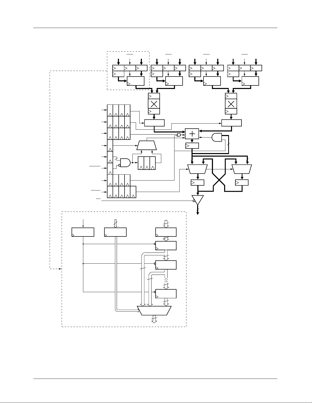
The TMC2249A utilizes a pipelined, bus-oriented structure
offering significant flexibility. Input register clock enables
and programmable input data pipeline delays on each port
offer an adaptable input structure for high-speed digital
systems. Following the multipliers, the user may perform
addition or subtraction of either product, arithmetic rounding
to 16 bits, and accumulation and summation of products with a
cascading input. The output port allows access to all 24 bits of
the internal accumulator by switching between overlapping
least and most-significant 16-bit words, and a three-state output enable simplifies connection to an external system bus.
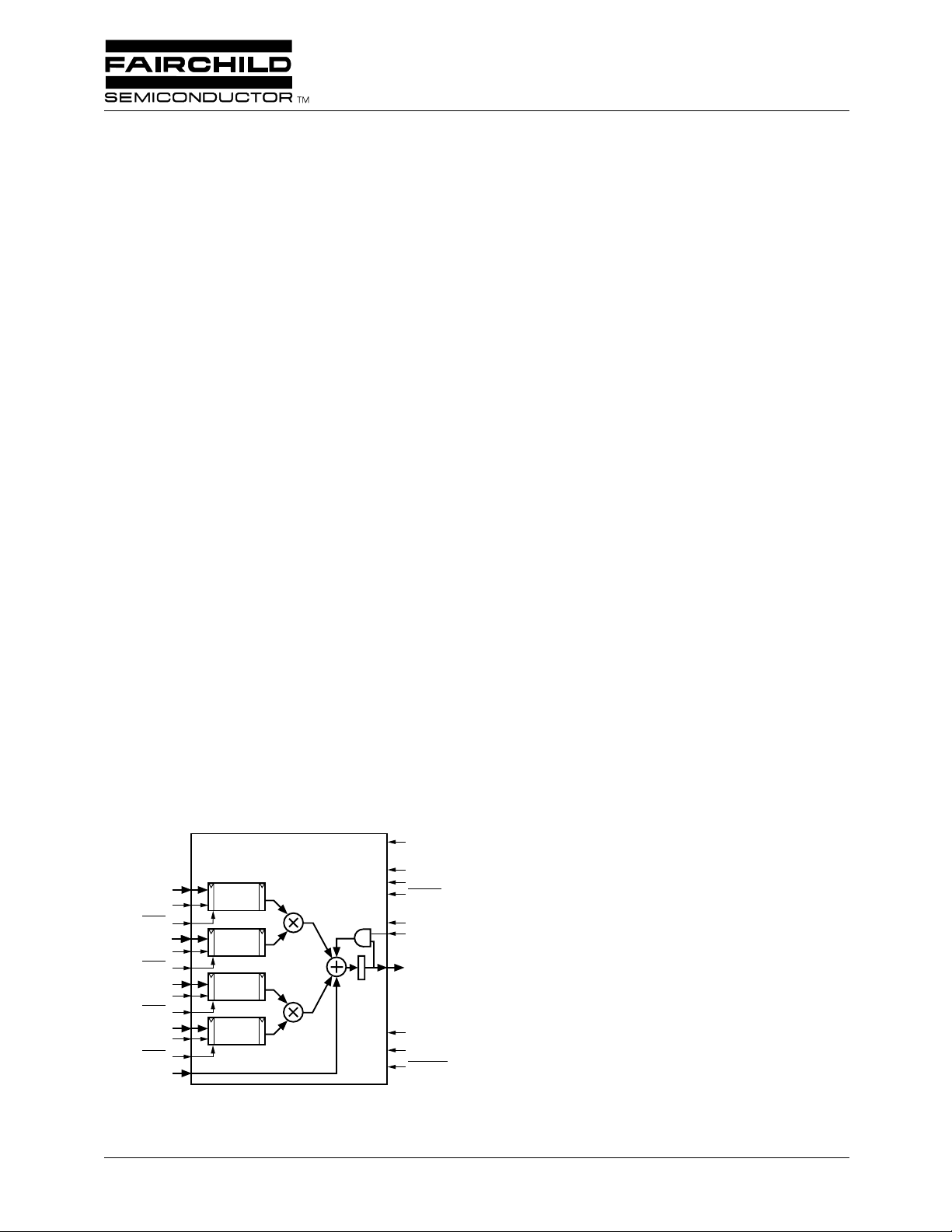
Logic Symbol
A
ADEL
B
BDEL
C
CDEL
D
DDEL
CAB
11-0
3-0
ENA
11-0
3-0
ENB
11-0
3-0
ENC
11-0
3-0
END
15-0
Delay
1-16
Delay
1-16
Delay
1-16
Delay
1-16
TMC2249A
Digital Mixer
CLK
NEG1
NEG2
SWAP
OE
ACC
S
15-0
RND
FT
CASEN
The TMC2249A has numerous applications in digital processing algorithms, from executing simple image mixing and
switching, to performing complex arithmetic functions and
complex waveform synthesis. FIR filters, digital quadrature
mixers and modulators, and vector arithmetic functions may
also be implemented with this device.
Fabricated in a submicron CMOS process, the TMC2249A
operates at guaranteed clock rates of up to 60 MHz over the
full temperature and supply voltage ranges. It is pin- and
function-compatible with Fairchild’s TMC2249, while providing higher speed operation and lower power dissipation. It
is available in a 120 pin Ceramic Pin Grid Array (CPGA),
120 pin Plastic Pin Grid Array (PPGA), 120 lead MQFP to
PPGA package (MPGA), and a 120 lead Metric Quad FlatPack (MQFP).
REV. 1.0.2 7/6/00
Page 2
PRODUCT SPECIFICATION TMC2249A
Block Diagram
ADEL
3-0
NEG1
NEG2
RND
FT
ADEL
16
3-0
CAS
15-0
CASEN
ACC
SWAP
OE
ENA
A
ENA BDEL
11-0
1-16
2's Comp 2's Comp
I0
3-0
A
ENB
11-0
1-16
124
B
11-0
3-0
ACC
16
M
01 01
16
S
15-0
11-0
1-16
C
ENC
DDEL
24
3-0
D
ENDCDEL
11-0
1-16
16
L
12
E
1
12
E
12
01 F
12 x (16:1) MUX
2
2
12
12
E
16
12
12
REV. 1.0.2 7/6/00
Page 3
TMC2249A PRODUCT SPECIFICATION
Functional Description
The TMC2249A performs the summation of products
described by the formula:
S(N+5) =A(N-ADEL) × B(N-BDEL) × (-1
C(N-CDEL) × D(N-DDEL) × (-1
NEG2(N)
NEG1(N)
) +
) +
CAS(N+3 × FT)
where ADEL through DDEL range from 1 to 16 pipe delays.
All inputs and controls utilize pipeline delay registers to
maintain synchronicity with the data input during that clock,
except when the Cascade data input is routed directly to the
accumulator by use of the Feedthrough control. One-half
LSB rounding to 16 bits may be performed on the sum of
products while summing with the cascade input data.
The user may access either the upper or lower 16 bits of the
24-bit accumulator by swapping overlapping registers. The
output bus has an asynchronous high-impedance enable, to
simplify interfacing to complex systems.
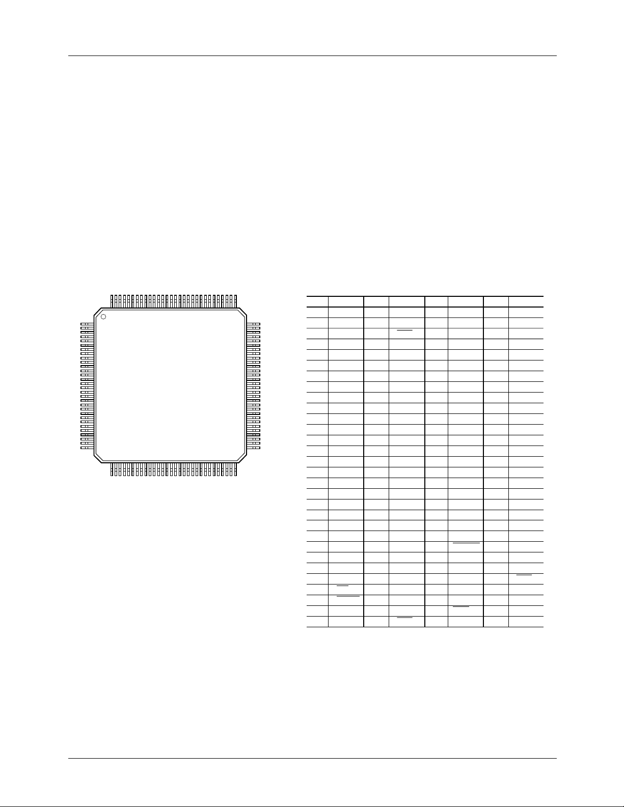
Pin Assignments
120 Pin Metric Quad Flat Pack, KE Package
120 91
1
30
31 60
90
61
Pin Name Pin Name
31
32
33
34
35
36
37
38
39
40
41
42
43
44
45
46
47
48
49
50
51
52
53
54
55
56
57
58
59
60
BDEL
BDEL
ENB
B
0
B
1
B
2
B
3
B
4
B
5
B
6
B
7
GND
B
8
B
9
B
10
V
DD
B
11
A
11
A
10
A
9
A
8
A
7
A
6
A
5
A
4
A
3
A
2
A
1
A
0
ENA
1
2
3
4
5
6
7
8
9
10
11
12
13
14
15
16
17
18
19
20
21
22
23
24
25
26
27
28
29
30
CLK
ACC
NEG1
NEG2
RND
S
15
S
14
GND
S
13
S
12
S
11
V
DD
S
10
S
9
S
8
GND
S
7
S
8
S
5
V
DD
S
4
S
3
S
2
GND
S
1
S
0
OE
SWAP
BDEL
BDEL
0
1
Pin Name Pin Name
61
62
63
64
65
66
67
68
69
70
71
72
73
74
75
76
77
78
79
80
81
82
83
84
85
86
87
88
89
90
ADEL
ADEL
ADEL
ADEL
NC
CAS
CAS
CAS
CAS
CAS
CAS
GND
CAS
CAS
CAS
CAS
CAS
CAS
CAS
CAS
CAS
CAS
CASEN
FT
CDEL
CDEL
CDEL
CDEL
ENC
C
2
3
91
3
92
2
93
1
94
0
95
96
15
97
14
98
13
99
12
100
11
101
10
102
103
9
104
8
105
7
106
6
107
5
108
4
109
3
110
2
111
1
112
0
113
114
115
0
116
1
117
2
118
3
119
120
0
C
1
C
2
C
3
C
4
C
5
C
6
C
7
C
8
C
9
C
10
C
11
V
DD
D
11
D
10
D
9
GND
D
8
D
7
D
6
D
5
D
4
D
3
D
2
D
1
D
0
END
DDEL
DDEL
DDEL
DDEL
3
2
1
0
REV. 1.0.2 7/6/00
3
Page 4
PRODUCT SPECIFICATION TMC2249A
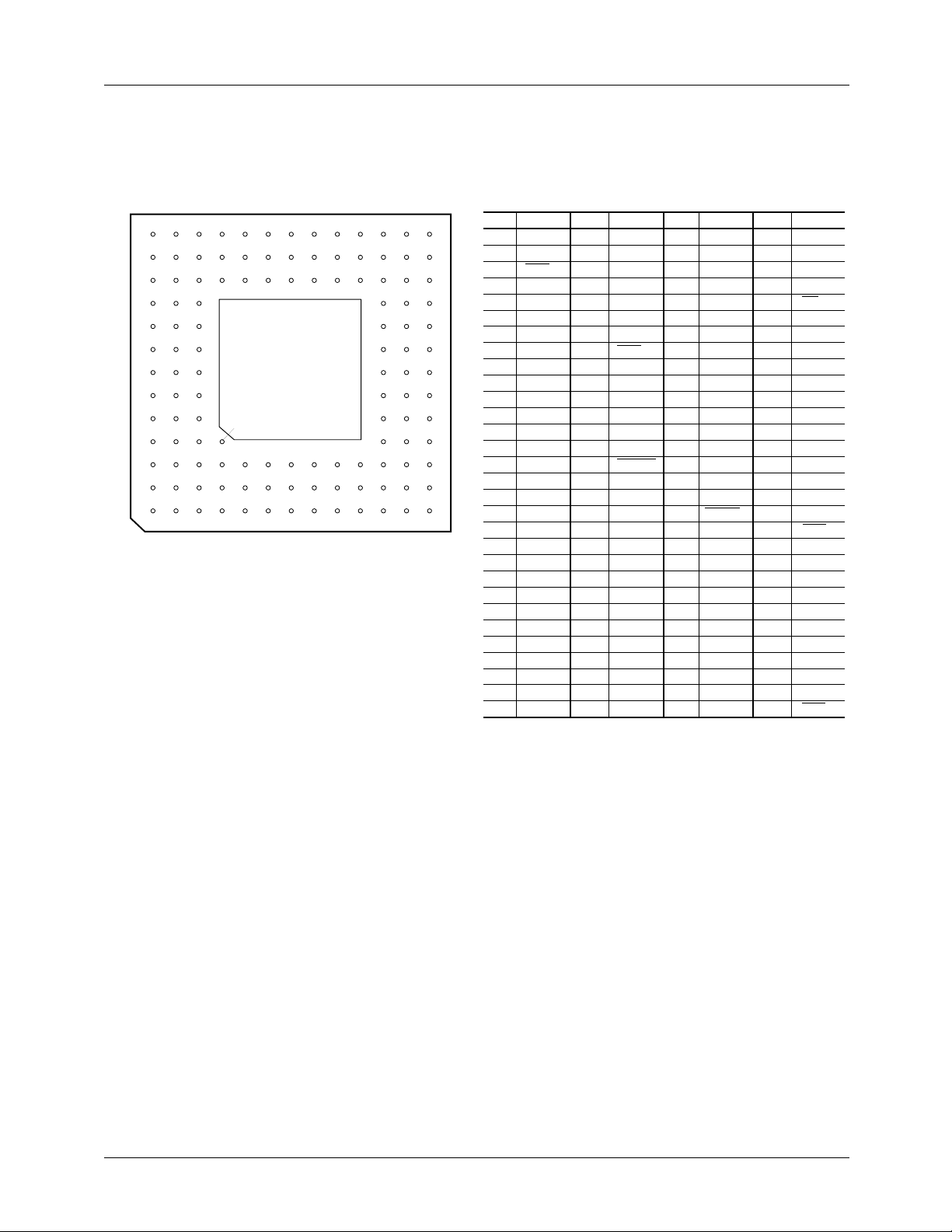
Pin Assignments
120 Pin Plastic Pin Grid Array, H5 Package, 120 Pin Ceramic Pin Grid Array, G1 Package, and
120 Pin Metric Quad FlatPack to 120 Pin Plastic Pin Array, H6 Package
13
12
11
10
9
8
7
6
5
4
3
2
1
BADEFGHJKLMNC
Top View
Cavity Up
KEY
Pin Name Pin Name
C5
C6
C7
C8
C9
C10
C11
C12
C13
D1
D2
D3
D11
D12
D13
E1
E2
E3
E11
E12
E13
F1
F2
F3
F11
F12
F13
G1
G2
G3
D
D
GND
V
C
C
C
ENC
CDEL
S
S
GND
CDEL
CDEL
CASEN
S
S
GND
FT
CAS
CAS
S
S
V
CAS
CAS
CAS
S
S
GND
A1
A2
A3
A4
A5
A6
A7
A8
A9
A10
A11
A12
A13
B1
B2
B3
B4
B5
B6
B7
B8
B9
B10
B11
B12
B13
C1
C2
C3
C4
DDEL
DDEL
END
D
2
D
4
D
7
D
8
D
10
C
11
C
9
C
6
C
3
C
0
NEG1
ACC
DDEL
D
0
D
3
D
6
D
9
D
11
C
10
C
7
C
5
C
2
CDEL
S
15
RND
CLK
DDEL
0
3
1
2
2
Pin Name Pin Name
G11
G12
G13
H1
H2
H3
H11
H12
H13
J1
J2
J3
J11
J12
J13
K1
K2
K3
K11
K12
K13
L1
L2
L3
L4
L5
L6
L7
L8
L9
CAS
CAS
CAS
S
6
S
5
V
DD
GND
CAS
CAS
S
4
S
3
GND
CAS
CAS
CAS
S
2
S
1
SWAP
ADEL
CAS
CAS
S
0
BDEL
BDEL
B
0
B
4
GND
V
DD
A
9
A
5
1
5
DD
8
4
1
1
13
14
3
0
11
12
0
1
9
10
DD
2
3
4
7
8
6
7
5
9
8
13
11
10
14
12
L10
A
L11
L12
L13
M1
M2
M3
M4
M5
M6
M7
M8
M9
M10
M11
M12
M13
N1
N2
0
N3
N4
N5
N6
0
N7
2
N8
N9
N10
N11
N12
N13
1
ADEL
NC
CAS
OE
BDEL
B
1
B
3
B
6
B
8
B
10
A
10
A
7
A
4
A
0
ADEL
ADEL
BDEL
ENB
B
2
B
5
B
7
B
9
B
11
A
11
A
8
A
6
A
3
A
2
ENA
3
15
3
2
1
1
4
REV. 1.0.2 7/6/00
Page 5

TMC2249A PRODUCT SPECIFICATION
Pin Descriptions
Pin Number
Pin Name
CPGA/PPGA/
MPGA
MQFP
Power
V
DD
GND E3, G3, J3, L6,
F3, H3, L7, C8 12, 20, 46, 102 Supply Voltage. The TMC2249A operates from a single +5V
8, 16, 24, 42,
H11, C7
72, 106
Clock
CLK C3 1
Inputs
A
11-0
N8, M8, L8,
N9, M9, N10,
L9, M10, N11,
48, 49, 50, 51,
52, 53, 54, 55,
56, 57, 58, 59
N12, L10, M11
B
11-0
N7, M7, N6,
M6, N5, M5,
N4, L5, M4,
47, 45, 44, 43,
41, 40, 39, 38,
37, 36, 35, 34
N3, M3, L4
C
11-0
A9, B9, A10,
C9, B10, A11,
B11, C10, A12,
101, 100, 99,
98, 97, 96, 95,
94, 93, 92, 91,
B12, C11, A13
D
11-0
B8, A8, B7, A7,
A6, B6, C6, A5,
B5, A4, C5, B4
103, 104, 105,
107, 108, 109,
110, 111, 112
113, 114, 115
ADEL
3-0
L11, M12,
61, 62, 63, 64 A-D Delay. ADEL through DDEL are the four-bit registered input
M13, K11
BDEL
CDEL
M2, L3, N1, L2 32, 31, 30, 29
3-0
3-0
D11, B13,
88, 87, 86, 85
C13, D12
DDEL
A2, C4, B3, A1 117, 118, 119,
3-0
120
CAS
15-0
L13, K12, J11,
K13, J12, J13,
H12, H13,
G12, G11,
66, 67, 68, 69,
70, 71, 73, 74,
75, 76, 77, 78,
79, 80, 81, 82
G13, F13, F12,
F11, E13, E12
Controls
S
15-0
C1, D2, D1,
E2, E1, F2, F1,
G2, G1, H1,
H2, J1, J2, K1,
6, 7, 9, 10, 11,
13, 14, 15, 17,
18, 19, 21, 22,
23, 25, 26
K2, L1
90
Pin Function Description
supply. All power and ground pins must be connected.
Ground. The TMC2249A operates from a single +5V supply. All
power and ground pins must be connected.
System Clock. The TMC2249A operates from a single master
clock input. The rising edge of clock strobes all enabled registers.
All timing specifications are referenced to the rising edge of CLK.
A-D Input. A through D are the four 12-bit registered data input
ports. A
-D
are the LSBs (see Table 1). Data presented to the input
0
0
ports is clocked in to the top of the 16-stage delay pipeline on the
next clock when enabled, "pushing" data down the register stack.
data pipe delay select word inputs. Data to be presented to the
multipliers is selected from one of sixteen stages in the input data
delay pipe registers, as indicated by the delay select word
presented to the respective input port during that clock. The
minimum delay is one clock (select word=0000), and the maximum
delay is 16 clocks (select word=1111). Following powerup these
values are indeterminate and must be initialized by the user.
Cascade Input. CAS is the 16-bit Cascade data input port. CAS
is
0
the LSB. See Table 1.
Sum Output. The current 16-bit result is available at the Sum
output. The output may be the most or least significant 16 bits of the
current accumulator output, as determined by SWAP. S
is the LSB.
0
See Table 1.
REV. 1.0.2 7/6/00
5
Page 6
PRODUCT SPECIFICATION TMC2249A
Pin Descriptions
Pin Number
Pin Name
Controls
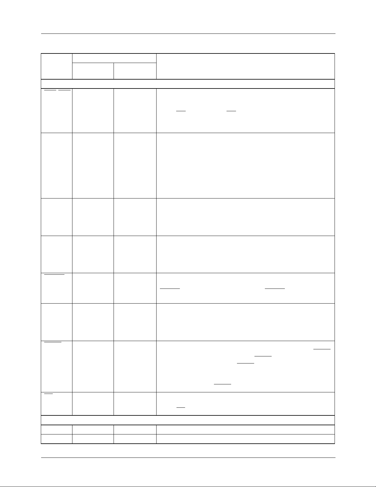
-END N13, N2, C12, A360, 33, 89, 116 Input Enables. Input data presented to port i11-0 (i=A,B,C, or D)
ENA
NEG1,2 B1, D3 3, 4
RND C2 5
CPGA/PPGA/
MPGA
FT E11 84
CASEN
ACC B2 2
SWAP K3 28
OE M1 27
No Connect
D13 83
L12 65 Do Not Connect
D4 Index Pin (optional)
(continued)
MQFP
Pin Function Description
are latched into delay pipeline i, and data already in pipeline i
advance by one register position, on each rising edge of CLK for
which ENi
move and the value at the input port i will be lost before it reaches
the multiplier.
Negate. The products of the multipliers are negated causing a
subtraction to be performed during the internal summation of
products, when the NEGate controls are HIGH, NEG1 negates the
product A x B, while NEG2 acts on the output of the multiplier which
generates the product C x D. When the length controls ADEL–
DDEL are set to zero, these controls indicate the operation to be
performed on data input during the same clock. As nonzero values
for ADEL–DDEL do not affect the pipelining of these controls, their
effect is not synchronous with the data input in these cases.
Round. When the rounding control is HIGH, the 24-bit sum of
products resulting from data input during that clock is rounded to 16
bits. When enabled rounding is automatically performed only during
the first cycle of each accumulation sequence, to avoid the
accumulation of roundoff errors.
Feedthrough. When the Feedthrough control is HIGH, the pipeline
delay through the cascade data path is minimized to simplify the
cascading of multiple devices. When FT is LOW and ADEL through
DDEL are all set to 0, the data inputs are aligned, such that
S(n+6) = CAS(n) + A(n)B(n) + C(n)D(n). See Table 2.
Cascade Enable. Data presented at the cascade data input port
are latched and accumulated internally when the input enable
CASEN during that clock is LOW. When CASEN is HIGH, the
cascade input port is ignored.
Accumulate. When the registered ACCumulator control is LOW, no
internal accumulation will be performed on the data input during the
current clock, effectively clearing the prior accumulated sum. When
ACC is HIGH, the internal accumulator adds the emerging product
to the sum of the previous products and RND is disabled.
Swap Output Words. The user may access both the most and
least-significant 16 bits of the 24-bit accumulator by utilizing SWAP.
Normal operation of the device, with SWAP = HIGH, outputs the
most significant word. Setting SWAP = LOW puts a double-register
structure into "toggle" mode, allowing the user to examine the LSW
on alternate clocks. New output data will not be clocked into the
output registers until SWAP returns HIGH.
Output Enable. Data currently in the output registers is available at
the output bus S
When OE is HIGH, the outputs are in the high-impedance state.
is LOW. When ENi is HIGH, the data in pipeline i do not
when the asynchronous Output Enable is LOW.
15-0
6
REV. 1.0.2 7/6/00
Page 7
TMC2249A PRODUCT SPECIFICATION
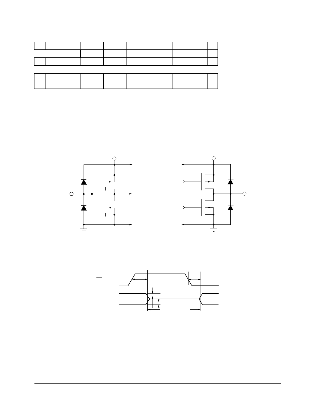
Table 1. Data Formats and Bit Weighting
1514131211109876543210BIT
11
10
9
8
7
6
5
4
3
2
1
-2
2
2
2
2
2
2
2
2
2
23
22
21
20
19
18
17
16
15
14
13
12
11
-2
2
2
2
2
2
2
2
2
2
2
2
15
14
13
12
11
10
9
8
7
6
5
2
2
2
2
2
2
2
2
2
2
4
2
2
2
3
2
10
2
22120
2
-223222221220219218217216215214213212211210292
Notes:
A minus sign indicates the two’s complement sign bit.
RND adds 1 to the 2
7
position if ACC is low.
2
2
9
0
2
DATA (A
8
2
CASCADE INPUT (CAS
SUM (S
15-0
11-0
)
LSW
8
MSW
-D
11-0
)
)
15-0
Equivalent Circuits and Threshold
Levels
V
DD
p
Data or
Control
Input
n
GND
Figure 1. Equivalent Digital Input Circuit
OE
Three-State
Outputs
t
DIS
0.5V
0.5V
Figure 2. Equivalent Digital Output Circuit
High Impedance
t
ENA
V
GND
2.0V
0.8V
DD
p
Output
n
REV. 1.0.2 7/6/00
Figure 3. Threshold Levels for Three-State Measurement
7
Page 8
PRODUCT SPECIFICATION TMC2249A
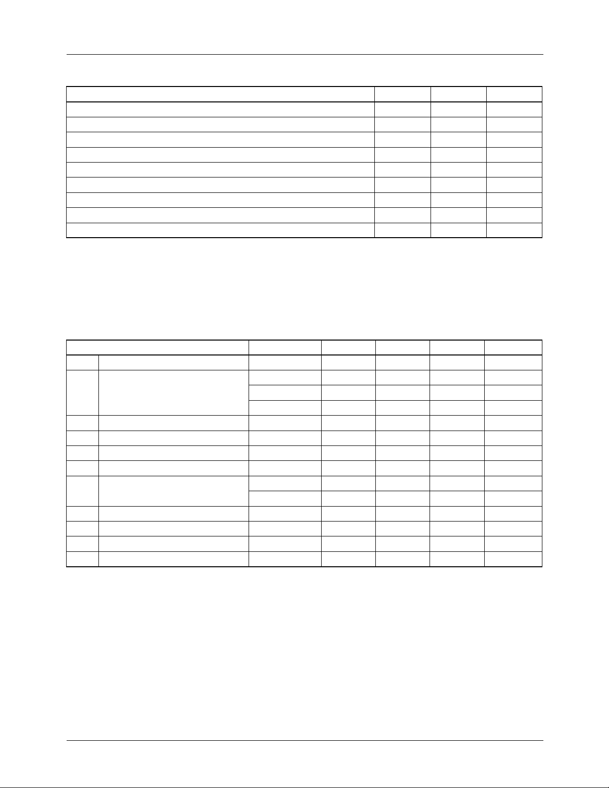
Absolute Maximum Ratings (beyond which the device may be damaged)1
Parameter Min Max Unit
Supply Voltage -0.5 7.0 V
Input Voltage -0.5 VDD + 0.5 V
Applied Voltage (Output)
Externally Forced Current (Output)
2
3,4
-0.5 VDD + 0.5 V
-3.0 6.0 mA
Output Short Circuit Duration (single output in HIGH state to ground) 1 sec
Operating, Ambient Temperature -20 110 °C
Operating, Junction Temperature 140 °C
Storage Temperature -65 150 °C
Lead, Soldering (10 seconds) 300 °C
Notes:
1. Functional operation under any of these conditions is NOT implied. Performance and reliability are guaranteed only if
Operating Conditions are not exceeded.
2. Applied voltage must be current limited to specified range.
3. Forcing voltage must be limited to specified range.
4. Current is specified as conventional current flowing into the device.
Operating Conditions
Parameter Min Nom Max Units
V
f
CLK
Power Supply Voltage 4.75 5.0 5.25 V
DD
Clock frequency TMC2249A 25 MHz
TMC2249A-1 40 MHz
TMC2249A-2 60 MHz
t
PWH
t
PWL
t
S
t
H
V
CLK pulse width, HIGH 6 ns
CLK pulse width, LOW 7 ns
Input Data Set-up Time 6 ns
Input Data Hold Time 1.5 ns
Input Voltage, Logic HIGH Data Inputs 2.0 V
IH
CLK Input 2.2 V
V
I
I
T
OH
OL
Input Voltage, Logic LOW 0.8 V
IL
Output Current, Logic HIGH -2.0 mA
Output Current, Logic LOW 4.0 mA
Ambient Temperature, Still Air 0 70 °C
A
8 REV. 1.0.2 7/6/00
Page 9
TMC2249A PRODUCT SPECIFICATION
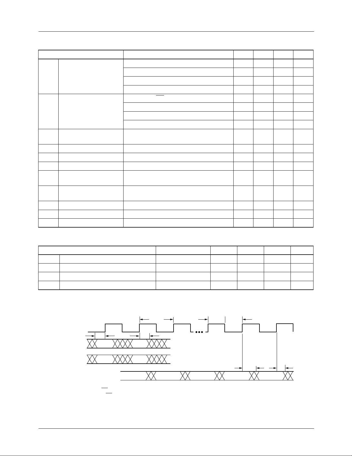
Electrical Characteristics
Parameter Conditions Min Typ Max Units
I
DD
I
DDU
I
DDQ
C
PIN
I
IH
I
IL
I
OZH
I
OZL
I
OS
V
OH
V
OL
Total Power Supply
Current
Power Supply Current,
Unloaded
Power Supply Current,
Quiescent
I/O Pin Capacitance 5 pF
Input Current, HIGH VDD = Max, VIN = V
Input Current, LOW VDD = Max, VIN = 0 V ±10 µA
Hi-Z Output Leakage
Current, Output HIGH
Hi-Z Output Leakage
Current, Output LOW
Short-Circuit Current -20 -80 mA
Output Voltage, HIGH S
Output Voltage, LOW S
= Max, C
V
DD
LOAD
= 25pF, f
CLK
= Max
TMC2249A 75 mA
TMC2249A-1 105 mA
TMC2249A-2 145 mA
V
= Max, OE = HIGH, f
DD
CLK
= Max
TMC2249A 68 mA
TMC2249A-1 92 mA
TMC2249A-2 124 mA
V
= Max, CLK = LOW 5 mA
DD
±10 µA
±10 µA
VDD = Max, VIN = V
DD
DD
VDD = Max, VIN = 0 V ±10 µA
, IOH = Max 2.4 V
15-0
, IOL = Max 0.4 V
15-0
Switching Characteristics
Parameter Conditions
t
DO
t
HO
t
ENA
t
DIS
Note:
1. All transitions are measured at a 1.5V level except for t
Output Delay Time C
Output Hold Time C
Three-State Output Enable Delay C
Three-State Output Disable Delay C
CLK
A
11-0
D
11-0
CONTROLS
S
15-0
t
S
DA DB
1
2
1
Except OE.
2
Assumes OE = LOW and ADEL-DDEL set to 0.
t
H
1/f
CLK
= 25 pF 14 ns
LOAD
= 25 pF 2.5 ns
LOAD
= 0 pF 12 ns
LOAD
= 0 pF 12 ns
LOAD
and t
ENA
DIS
1
.
Min Typ Max Units
t
PWHtPWL
5321
67
t
DO
SA
t
HO
Figure 4. Timing Diagram
REV. 1.0.2 7/6/00 9
Page 10
PRODUCT SPECIFICATION TMC2249A
Application Notes
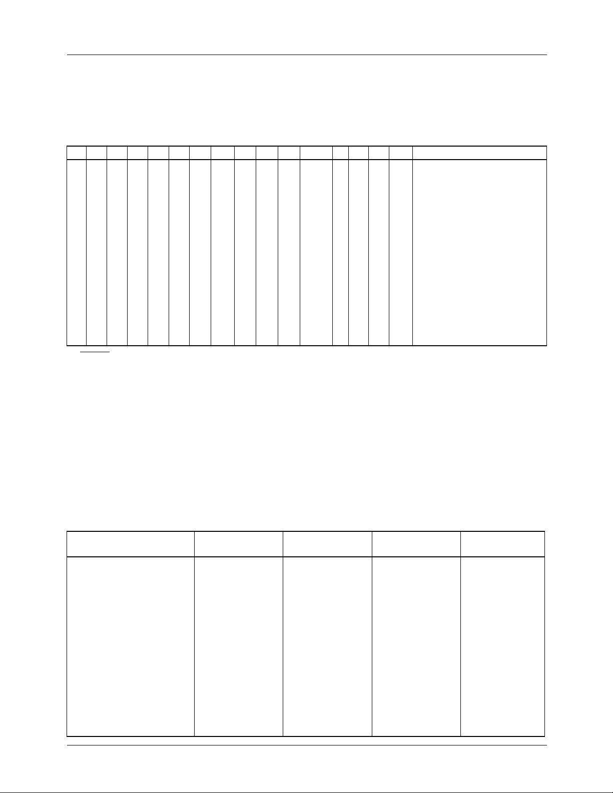
The TMC2249A is a flexible signal and image processing building block with numerous user-selectable functions which
expand its usefulness. Table 2 clarifies the operation of the device, demonstrating the various feature available to the user and
the timing delays incurred.
Table 2. TMC2249A Operation Sequence
CLK ADEL A
1 0 A(1) 0 B(1) 0 C(1) 0 D(1) L L 0 L L H H —
2 0 A(2) 0 B(2) 0 C(2) 0 D(2) L H 0 L L H H —
3 0 A(3) 0 B(3) 0 C(3) 0 D(3) H L 0 L L L H —
4 0 A(4) 0 B(4) 0 C(4) 0 D(4) L L CAS(4) L L L H —
5 0 A(5) 0 B(5) 0 C(5) 0 D(5) L L 0 L L L H —
6 0 A(6) 0 B(6) 0 C(6) 0 D(6) L L 0 L L H H (A(1) × B(1)+C(1) × D(1)+27)
7 0 A(7) 0 B(7) 0 C(7) 0 D(7) L L 0 L H X H (A(2) × B(2)-C(2) × D(2)+27)
8 0 A(8) 0 B(8) 0 C(8) 0 D(8) L L CAS(8) H L L L (-A(3) × B(3)+C(3) × D(3))
9 0 A(9) 0 B(9) 0 C(9) 0 D(9) L L 0 L L H H (A(4) × B(4)+C(4) × D(4)+CAS(4))
10 (A(5) × B(5)+C(5) × D(5)+CAS(8))
11 (A(6) × B(6)+C(6) × D(6)+27)
12 (A(7) × B(7)+C(7) × D(7)+S(11))
13 (S(12))
14 (A(9) × B(8)+C(7) × D(6)+27)
CASEN = 0, H=HIGH, L=LOW, “ms” indicates most significant output word (bits 23-8), “ls” indicates least significant word (bits
15-0). The appropriate enables for the indicated data are assumed, otherwise ‘-’ indicates that port not enabled. Note that the
output data summations including A(8)-D(8) is lost, since the output on cycle 13 is swapped to the LSW of S(12) on cycle 8.
In general, RND may be left high unless the ls output is to be used, as on line 8 above.
11-0
BDEL B
11-0
CDEL C
11-0
DDEL D
NEG1 NEG2 CAS
11-0
FT ACC RND SWAP S
15-0
15-0
ls
ms
ms
ms
ms
ms
ms
ms
ms
Digital Filtering
The input structure of the TMC2249A demonstrates great
versatility when all four multiplier inputs and the programmable delay registers are utilized.
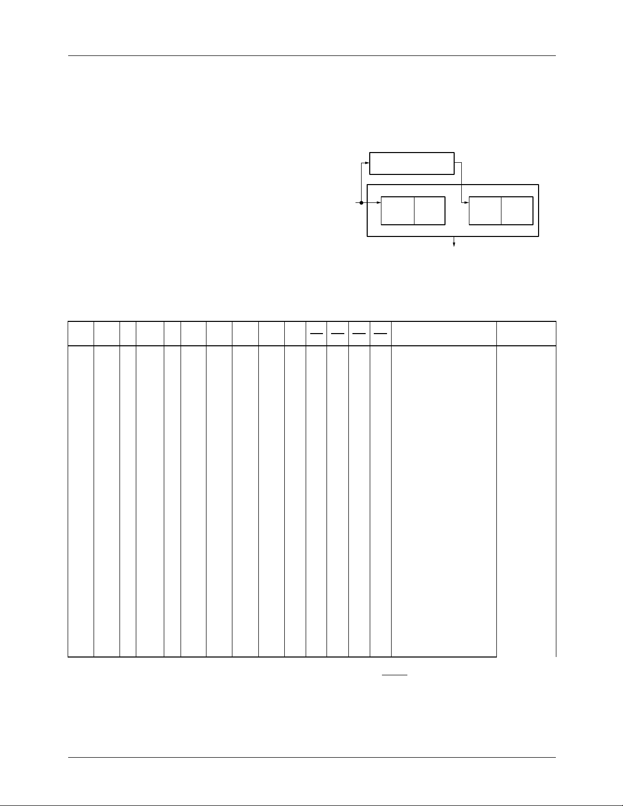
Table 3 and Table 4 illlustrate how a direct-form symmetric
FIR filter of up to 32 taps can be implemented. By utilizing
the four input delay registers as pipelined storage banks, the
user can store up to 32 coefficient-data word pairs, split into
alternate "even" and "odd" halves. Two taps of the filter are
calculated on each clock, and the user then increments/decrements the delay words (ADEL-DDEL). The sums of products are successively added to the global sum in the internal
accumulator.
Table 3. FIR Filtering with the TMC2249A—Initial Data Loading
Even Data Odd Data Coefficient Storage
Register Position (Hex) A C B D
0 x(31) x(30) h(0) h(1)
1 x(29) x(28) h(2) h(3)
2 x(27) x(26) h(4) h(5)
3 x(25) x(24) h(6) h(7)
4 x(23) x(22) h(8) h(9)
5 x(21) x(20) h(10) h(11)
6 x(19) x(18) h(12) h(13)
7 x(17) x(16) h(14) h(15)
8 x(15) x(14) h(15) h(14)
9 x(13) x(12) h(13) h(12)
A x(11) x(10) h(11) h(10)
B x(9) x(8) h(9) h(8)
C x(7) x(6) h(7) h(6)
D x(5) x(4) h(5) h(4)
E x(3) x(2) h(3) h(2)
F x(1) x(0) h(1) h(0)
10 REV. 1.0.2 7/6/00
Page 11
TMC2249A PRODUCT SPECIFICATION
Once all of the products of the desired taps have been
summed, the result is available at the output. The user then
"pushes" a new time-data sample on to the appropriate even
or odd data register "stack" and reiterates the summation.
Note that the coefficient bank "pointers", the BDEL and
DDEL delay words, are alternately incremented and decre-
As shown in Figure 5, the data is then sent to the C input,
thus "stacking" the A and C delay registers to create a single
N-tap FIR filter. The incremented delay words (ADELDDEL) for all four inputs are identical. Again, the filter
throughput is equal to the clock speed divided by one-half
the number of taps implemented.
mented on successive filter passes to maintain alignment
between the incoming data samples and their respective
coefficients.
The effective filter speed is calculated by dividing the clock
rate by one-half the number of taps implemented.
Alternatively , non-symmetric FIR filters can be implemented
using the TMC2249A in a similar fashion. Here, a shift register is used to delay the incoming data fed to the A input by
an amount equal to one-half the length of the filter (the
x(m)
TMC2011A
16-Stage Shift Register
AB CD
x(m+0)
x(m+15) h(15) x(m+31)
h(0) x(m+16) h(16)
S
15-0
Filter Output
TMC2249A
h(31)
length of the A delay register).
Figure 5. Non-Symmetric 32-Tap FIR Filtering Using the
TMC2249A
Table 4. FIR Filtering – Operation Sequence
Push
Cycle
AB
1 – – – – 0 0 0 0 L H H H H x(31)•h(0)+x(30)•h(1) See Note 2
2 – – – – 1 1 1 1 H H H H H +x(29)•h(2)+x(28)•h(3)
3 – – – – 2 2 2 2 H H H H H +x(27)•h(4)+x(26)•h(5)
4 – – – – 3 3 3 3 H H H H H +x(25)•h(6)+x(24)•h(7)
5 – – – – 4 4 4 4 H H H H H +x(23)•h(8)+x(22)•h(9)
6 – – – – 5 5 5 5 H H H H H +x(21)•h(10)+x(20)•h(11)
7 – – – – 6 6 6 6 H H H H H +x(19)•h(12)+x(18)•h(13)
8 – – – – 7 7 7 7 H H H H H +x(17)•h(14)+x(16)•h(15)
9 – – – – 8 8 8 8 H H H H H +x(15)•h(15)+x(14)•h(14)
10 – – – – 9 9 9 9 H H H H H +x(13)•h(13)+x(12)•h(12)
11 – – – – A A A A H H H H H +x(11)•h(11)+x(10)•h(10)
12 – – – – B B B B H H H H H +x(9)•h(9)+x(8)•h(8)
13 – – – – C C C C H H H H H +x(7)•h(7)+x(6)•h(6)
14 – – – – D D D D H H H H H +x(5)•h(5)+x(4)•h(4)
15 – – – – E E E E H H H H H +x(3)•h(3)+x(2)•h(2)
16 – – x(32) – F F F F H H H L H +x(1)•h(1)+x(0)•h(0)
17 – – – – 0 0 F F H H H H H +x(31)•h(1)+x(32)•h(0)
18 – – – – 1 1 E E H H H H H +x(29)•h(3)+x(30)•h(2)
19 – – – – 2 2 D D H H H H H +x(27)•h(5)+x(28)•h(4)
20 – – – – 3 3 C C H H H H H +x(25)•h(7)+x(26)•h(6)
21 – – – – 4 4 B B H H H H H +x(23)•h(9)+x(24)•h(8)
•
•
Push
C D ADEL CDEL BDEL DDEL ACC ENA ENB ENC END Convolutional Sum
Resultant
Output
Notes:
1. If only the 16 MSBs of the result are used, the user may leave RND HIGH and SWAP
low. If the 16 LSBs or all 24 bits of the
result are used, then RND should be set low.
15
sxk()hk() xk 16+()hk()+()
2.
=
∑
K0=
REV. 1.0.2 7/6/00 11
Page 12
PRODUCT SPECIFICATION TMC2249A
Complex Arithmetic Functions
The TMC2249A can also be used to perform complex arithmetic functions. The basic function performed by the device,
ignoring the delay controls,
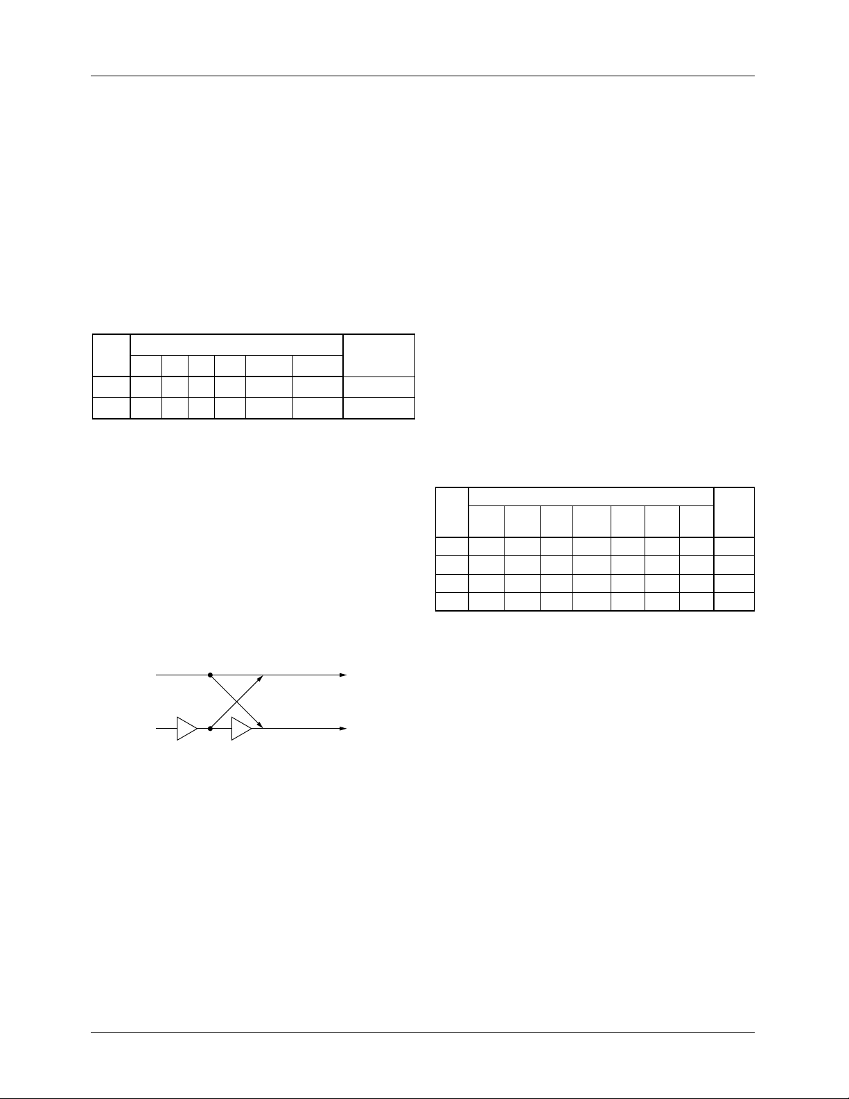
SUM = (±A•B) + (±C•D)
can realize in two steps the familiar summation:
(P+jR)(S+jT)=(PS-RT) + j(PT+SR)
(1) (2)
by loading the TMC2249A as follows:
TMC2249A Inputs
Step A B C D NEG1 NEG2
1 P S R T L H (PS-RT)
2 P T R S L L (PT+SR)
where H and L indicate a logic HIGH and LOW.
Thus we can perform a complex multiplication in two clock
cycles. Notice that the user must switch the two components
of the second input vector between the B and D inputs to
obtain the second complex summation.
Calculating a Butterfly
Taking advantage of the complex multiply which we implemented above using the TMC2249A, we can expand slightly
to calculate a Radix-2 Butterfly, the core of the Fast Fourier
Transform algorithm. To review, the Butterfly is calculated
as shown in Figure 6.
Resultant
Output
XA
Expanding the complex vectors A and B to calculate X and
Y, we get:
X = (Re(A)+jlm(A))+(Re(B)Re(W)lm(B)lm(W)+j(Re(B)lm(W)+lm(B)Re(W)))
= (Re(A)+Re(B)Re(W)-
lm(B)lm(W))+j(lm(A)+Re(B)lm(W)+lm(B)Re(W))
= Re(X)+jlm(X)
and,
Y = (Re(A)+jlm(A))-(Re(B)Re(W)lm(B)lm(W)+j(Re(B)lm(W)+lm(B)Re(W)))
= (Re(A)Re(B)Re(W)+lm(B)lm(W))+j(lm(A)-Re(B)lm(W)lm(B)Re(W))
= Re(Y)+jlm(Y)
The butterfly is then neatly implemented in four clocks, as
follows:
TMC2249A Inputs
Step
ABCD
1 Re(B) Re(W) Im(B) Im(W) Re(A) L H Re(X)
2 Re(B) Re(W) Im(B) Im(W) Re(A) H L Re(Y)
3 Re(B) Im(W) Im(B) Re(W) Im(A) L L Im(X)
4 Re(B) Im(W) Im(B) Re(W) Im(A) H H Im(Y)
CAS
Input
NEG1 NEG2
Result-
ant
Output
Notice again that the components of the second vector must
be switched by the user on the second half of the computation, as well as the parts of the vector presented to the cascade input.
r
W
B
N
-1
Y
Quadrature Modulation
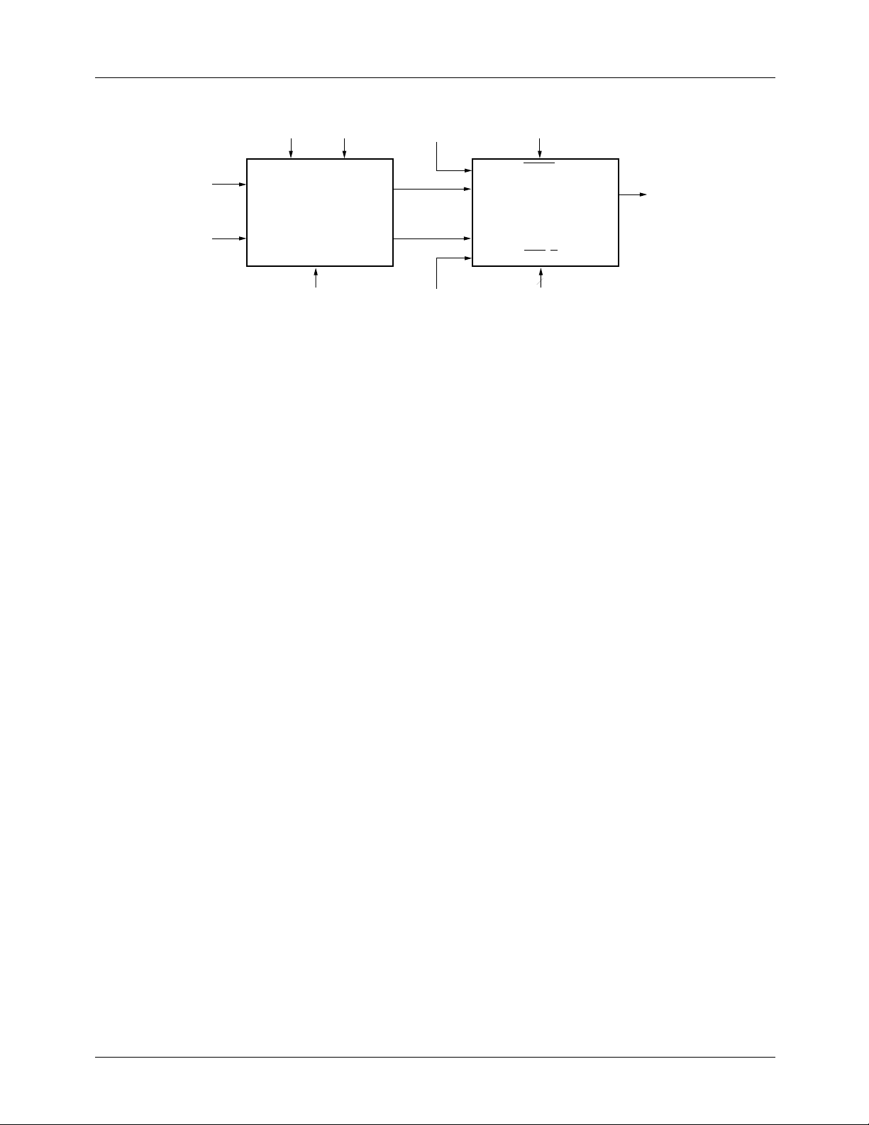
The TMC2249A can also be used to advantage as a digitaldomain complex frequency synthesizer, as demonstrated in
Figure 6. Signal Flow of Radix-2 Butterfly
Figure 7.
Where
X=A+B(W
Y=A–B(W
and W
r
)
N
r
),
N
r
is the complex phase coefficient, or "twiddle factor"
N
for the N-point transform, which is:
r
W
=e
N
j(2π/N)
= cos(2π/N) + j(sin(2π/N))
= Re(W) + jIm(W)
Here, orthogonal sinusoidal waveforms are generated digitally in the TMC2330A Coordinate Transformer. These
quadrature phase coefficients are then multiplied with two
input signals, such as digitized analog data.
The TMC2249A then adds these products, which can be output directly to a high-speed digital-to-analog converter such
as the Fairchild TDC1012 for direct waveform synthesis.
This 12-bit, 20MHz DAC is ideally suited to waveform generation, featuring extremely low glitch energy for low spurious harmonics and distortion.
with Re and Im indicating the real and imaginary parts of the
vector.
12 REV. 1.0.2 7/6/00
Page 13
TMC2249A PRODUCT SPECIFICATION
0
RTP TCXY
A = Mixer
Amplitude
F = Mixer
Frequency
XRIN
YPIN
RXOUT(15:4)
TMC2330A TMC2249A
PYOUT(15:4)
ACC
01
Figure 7. Direct Quadrature Waveform Synthesizer using the TMC2249A and TMC2330A
Related Products
• TMC2301 Image Resampling Sequencer
• TMC2302A Image Manipulation Sequencer
• TMC2246A Image Filter
• TMC2242B Half–Band Filter
1
I = Signal 1
Q = Signal 2
A
B
C
D
[11:0]
[11:0]
1
SWAP
ENA-D
0
S
15-0
4
Output = A *
(I*cos(wt)
+Q*sin(wt))
REV. 1.0.2 7/6/00 13
Page 14
TMC2249A PRODUCT SPECIFICATION
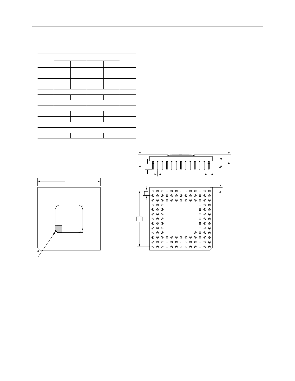
Mechanical Dimensions
120-Lead CPGA Package
Symbol
A .080 .160 2.03 4.06
A1 .040 .060 1.01 1.53
A2 .125 3.17
øB .016 .020 0.40 0.51
øB2
D 1.340 1.380 33.27 35.05
D1
e
L
L1 .170 .190 4.31 4.83
M13 13
N
P
Inches
Min. Max. Min. Max.
.215 5.46
.050 NOM. 1.27 NOM.
1.200 BSC 30.48 BSC
.100 BSC 2.54 BSC
.110 .145 2.79 3.68
120 120
.003 — .076 —
D
Millimeters
Notes
2
2
SQ
3
4
A2
Notes:
1.
Pin #1 identifier shall be within shaded area shown.
2.
Pin diameter excludes solder dip finish.
3.
Dimension "M" defines matrix size.
4.
Dimension "N" defines the maximum possible number of pins.
5.
Orientation pin is at supplier's option.
6.
Controlling dimension: inch.
A1
L
e
øB
øB2
P
A
Top View
Cavity Up
Pin 1 Identifier
D1
REV. 1.0.2 7/6/00 14
Page 15
TMC2249A PRODUCT SPECIFICATION
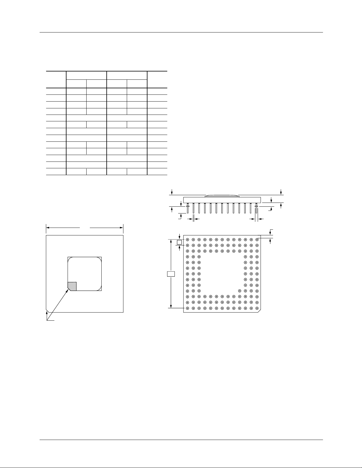
Mechanical Dimensions
120-Lead PPGA Package
Symbol
A .080 .160 2.03 4.06
A1 .040 .060 1.01 1.53
A2 .125 3.17
øB .016 .020 0.40 0.51
øB2
D 1.340 1.380 33.27 35.05
D1
e
L
L1 .170 .190 4.31 4.83
M13 13
N
P
Inches
Min. Max. Min. Max.
.215 5.46
.050 NOM. 1.27 NOM.
1.200 BSC 30.48 BSC
.100 BSC 2.54 BSC
.110 .145 2.79 3.68
120 120
.003 — .076 —
D
Millimeters
Notes
2
2
SQ
3
4
A2
Notes:
1.
Pin #1 identifier shall be within shaded area shown.
2.
Pin diameter excludes solder dip finish.
3.
Dimension "M" defines matrix size.
4.
Dimension "N" defines the maximum possible number of pins.
5.
Orientation pin is at supplier's option.
6.
Controlling dimension: inch.
A1
L
e
øB
øB2
P
A
Top View
Cavity Up
Pin 1 Identifier
D1
REV. 1.0.2 7/6/00 15
Page 16
PRODUCT SPECIFICATION TMC2249A
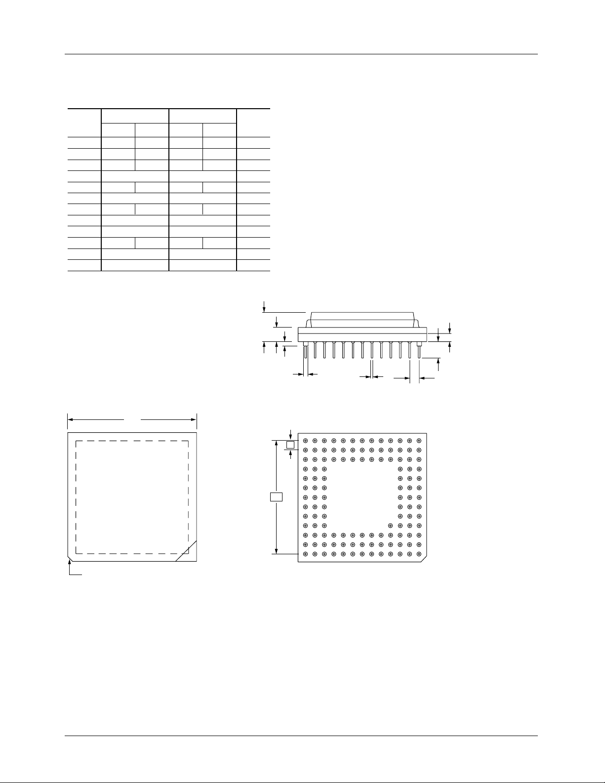
Mechanical Dimensions
120-Lead Metric Quad Flat Package to Pin Grid Array Package (MPGA)
Symbol
A .309 .311 7.85 7.90
A1 .145 .155 3.68 3.94
A2
A3
øB .016 .020 0.40 0.51
øB2
D 1.355 1.365 34.42 34.67
D1
e
L
M13 13
N
Inches
Min. Max. Min. Max.
.080 2.03
.175 .185 4.45 4.70
.090 2.29
.050 TYP. 1.27 TYP.
.050 NOM. 1.27 NOM.
1.200 BSC 30.48 BSC
.100 BSC 2.54 BSC
120 120
Millimeters
Notes
2
2
SQ
3
4
Notes:
1.
Pin #1 identifier shall be within shaded area shown.
2.
Pin diameter excludes solder dip finish.
3.
Dimension "M" defines matrix size.
4.
Dimension "N" defines the maximum possible number of pins.
5.
Orientation pin is at supplier's option.
6.
Controlling dimension: inch.
A
A1
A3
øB2
øB
e
A2
L
Fairchild
TMC2249A
Pin 1 Identifier
D
e
D1
16 REV. 1.0.2 7/6/00
Page 17
TMC2249A PRODUCT SPECIFICATION
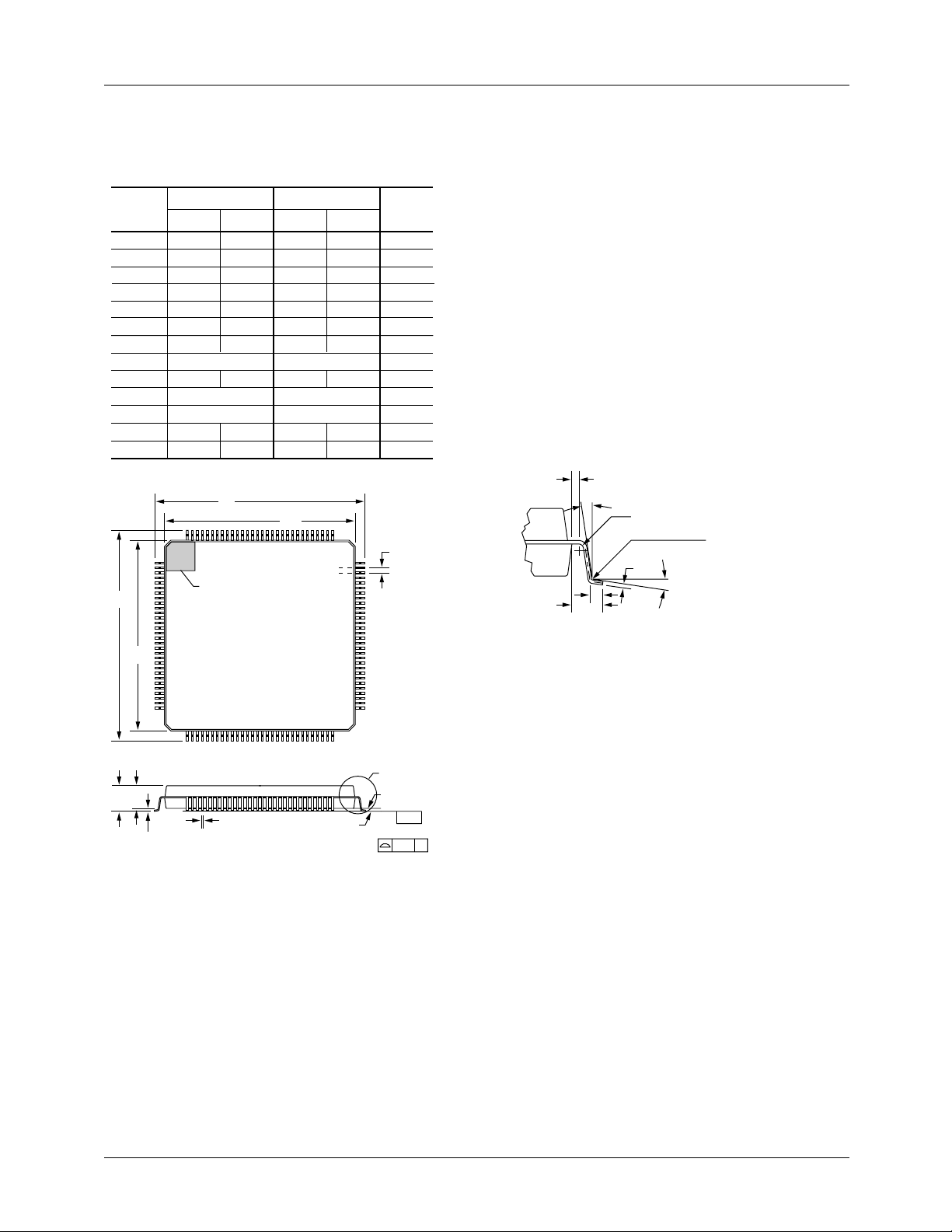
Mechanical Dimensions
120-Lead MQFP Package
Symbol
A — .154 — 3.92
A1 .010 — .25 —
A2 .125 .144 3.17 3.67
B .012 3, 5.30
C .005 .13
D/E 1.219 1.238 30.95 31.45
D1/E1 1.098 1.106 27.90 28.10
e
L .026 .037 .65 .95
N
ND
α 0° 7° 0° 7°
ccc
E
E1
Inches
Min. Max. Min. Max.
.018 .45
.009 .23
.0315 BSC .80 BSC
120 120
30 30
— .004 — .10
D
PIN 1 IDENTIFIER
Millimeters
D1
Notes
5
4
e
0.063" Ref (1.60mm)
Notes:
1.
All dimensions and tolerances conform to ANSI Y14.5M-1982.
2.
Controlling dimension is millimeters.
3.
Dimension "B" does not include dambar protrusion. Allowable
dambar protrusion shall be .08mm (.003in.) maximum in excess
of the "B" dimension. Dambar cannot be located on the lower
radius or the foot.
4.
"L" is the length of terminal for soldering to a substrate.
5.
"B" & "C" includes lead finish thickness.
.20 (.008) Min.
0° Min.
.13 (.005) R Min.
.13/.30
.005/.012
C
L
Lead Detail
R
α
See Lead Detail
A2
A
B
A1
Seating Plane
Base Plane
-C-
LEAD COPLANARITY
ccc
C
REV. 1.0.2 7/6/00 17
Page 18

PRODUCT SPECIFICATION TMC2249A
Ordering Information
Product
Number
Temperature
Range
Speed
Grade
Screening Package
Package
Marking
TMC2249AG1C 0°C to 70°C 25 MHz Commercial 120 Pin Ceramic Pin Grid Array 2249AG1C
TMC2249AG1C1 0°C to 70°C 40 MHz Commercial 120 Pin Ceramic Pin Grid Array 2249AG1C1
TMC2249AG1C2 0°C to 70°C 60 MHz Commercial 120 Pin Ceramic Pin Grid Array 2249AG1C2
TMC2249AH5C 0°C to 70°C 25 MHz Commercial 120 Pin Plastic Pin Grid Array 2249AH5C
TMC2249AH5C1 0°C to 70°C 40 MHz Commercial 120 Pin Plastic Pin Grid Array 2249AH5C1
TMC2249AH5C2 0°C to 70°C 60 MHz Commercial 120 Pin Plastic Pin Grid Array 2249AH5C2
TMC2249AH6C 0°C to 70°C 25 MHz Commercial 120 Lead Metric Quad Flat Pack
N/A
to Pin Grid Array
TMC2249AH6C1 0°C to 70°C 40 MHz Commercial 120 Lead Metric Quad Flat Pack
N/A
to Pin Grid Array
TMC2249AH6C2 0°C to 70°C 60 MHz Commercial 120 Lead Metric Quad Flat Pack
N/A
to Pin Grid Array
TMC2249AKEC 0°C to 70°C 25 MHz Commercial 120 Lead Metric Quad Flat Pack 2249AKEC
TMC2249AKEC1 0°C to 70°C 40 MHz Commercial 120 Lead Metric Quad Flat Pack 2249AKEC1
TMC2249AKEC2 0°C to 70°C 60 MHz Commercial 120 Lead Metric Quad Flat Pack 2249AKEC2
LIFE SUPPORT POLICY
FAIRCHILD’S PRODUCTS ARE NOT AUTHORIZED FOR USE AS CRITICAL COMPONENTS IN LIFE SUPPORT DEVICES
OR SYSTEMS WITHOUT THE EXPRESS WRITTEN APPROVAL OF THE PRESIDENT OF FAIRCHILD SEMICONDUCTOR
CORPORATION. As used herein:
1. Life support devices or systems are devices or systems
which, (a) are intended for surgical implant into the body, or
(b) support or sustain life, and (c) whose failure to perform
when properly used in accordance with instructions for use
provided in the labeling, can be reasonably expected to
result in a significant injury of the user.
www.fairchildsemi.com
2. A critical component in any component of a life support
device or system whose failure to perform can be
reasonably expected to cause the failure of the life support
device or system, or to affect its safety or effectiveness.
7/6/00 0.0m 002
2000 Fairchild Semiconductor Corporation
Stock#DS30002249A
 Loading...